SlideShare a Scribd company logo
1 of 119
Download to read offline
UNIT-5: MICROPROCESSOR (ARCHITECTURE AND PROGRAMMING -8086-16 BIT)
5.1 INTRODUCTION:
 8086 Microprocessor is an enhanced version of 8085Microprocessor that was
designed by Intel in 1976.
 It is a 16-bit Microprocessor having 20 address lines and16 data lines that
provides up to 1MB storage.
 It consists of powerful instruction set, which provides operations like
multiplication and division easily.
 It supports two modes of operation, i.e. Maximum mode and Minimum mode.
 Maximum mode is suitable for system having multiple processors and Minimum
mode is suitable for system having a single processor.
5.2 8086 MICROPROCESSOR FEATURES:
 It is 16-bit microprocessor
 It has a 16-bit data bus, so it can read data from or write data to memory and
ports either 16-bit or 8-bit at a time.
 It has 20 bit address bus and can access up to 220 memory locations (1MB).
 It can support up to 64K I/O ports
 It provides 14, 16-bit registers
 It has multiplexed address and data bus AD0-AD15 & A16-A19
 It requires single phase clock with 33% duty cycle to provide internal timing.
 Pre fetches up to 6 instruction bytes from memory and queues them in order to
speed up theprocessing.
 8086 supports 2 modes of operation
1. Minimum mode
2. Maximum mode
 It is available in 3 versions based on the frequency of operation −
1. 8086 → 5MHz
2. 8086-2 → 8MHz
3. (c)8086-1 → 10 MHz
 It uses two stages of pipelining, i.e. fetch Stage and Execute Stage, which
improves performance.
 Fetch stage can pre fetch up to 6 bytes of instructions and stores them in the
queue.
 Execute stage executes these instructions.
 It has 256 vectored interrupts.
 It consists of 29,000 transistors.
5.3 REGISTER ORGANIZATION:
 8086 has a powerful set of registers known as general purpose registers and
special purposeregisters.
 All of them are 16-bit registers.
 General purpose registers:
 These registers can be used as either 8-bit registers or 16-bit registers.
 They may be either used for holding data, variables and intermediate results
temporarily or for other purposes like a counter or for storing offset address
for some particular addressing modes etc.
 Special purpose registers:
 These registers are used as segment registers, pointers, index registers or as
offset storage registers for particular addressing modes.
 The 8086 registers are classified into the following types:
 General Data Registers
 Segment Registers
 Pointers and Index Registers
 Flag Register
1. General Data Registers:
 The registers AX, BX, CX and DX are the general purpose 16-bit registers.
 AX is used as 16-bit accumulator. The lower 8-bit is designated as AL and
higher 8-bit is designated as AH.
 AL Can be used as an 8-bit accumulator for 8-bit operation.
 All data register can be used as either 16 bit or 8 bit. BX is a 16 bit register,
but BL indicates the lower 8-bitof BX and BH indicates the higher 8-bit of BX.
 The register BX is used as offset storage for forming physical address in case
of certain addressing modes.
 The register CX is used default counter in case of string and loop instructions.
 DX register is a general purpose register which may be used as an implicit
operand or destination in case of a few instructions.
2. Segment Registers:
 There are 4 segment registers. They are:
 Code Segment Register(CS)
 Data Segment Register(DS)
 Extra Segment Register(ES)
 Stack Segment Register(SS)
 The 8086 architecture uses the concept of segmented memory. 8086 able
to address a memory capacity of 1 megabyte and it is byte organized. This 1
megabyte memory is divided into 16 logical segments. Each segment
contains 64 Kbytes of memory.
 Code segment register (CS):
It is used for addressing memory location in the code segment of the
memory, where the executable program is stored.
 Data segment register (DS):
It points to the data segment of the memory where the data is stored.
 Extra Segment Register (ES) :
It also refers to a segment in the memory which is another data segment in
the memory.
 Stack Segment Register (SS):
 It is used for addressing stack segment of the memory. The stack segment
is that segment of memory which is used to store stack data.
 While addressing any location in the memory bank, the physical address
is calculated from two parts:
Physical address= segment address + offset address
 The first is segment address, the segment registers contain 16-bit
segment base addresses, related to different segment.
 The second part is the offset value in that segment.
3. Pointers and Index Registers:
 The index and pointer registers are given below:
 IP—Instruction pointer-store memory location of next instruction to be
executed
 BP—Base pointer
 SP—Stack pointer
 SI—Source index
 DI—Destination index
 The pointers registers contain offset within the particular segments.
 The pointer register IP contains offset within the code segment.
 The pointer register BP contains offset within the data segment.
 Thee pointer register SP contains offset within the stack segment.
 The index registers are used as general purpose registers as well as for offset
storage in case of indexed, base indexed and relative base indexed addressing
modes.
 The register SI is used to store the offset of source data in data segment.
 The register DI is used to store the offset of destination in data or extra
segment.
 The index registers are particularly useful for string manipulation.
4. 8086 flag register and its functions:
 The 8086 flag register contents indicate the results of computation in the ALU.
It also contains some flag bits to control the CPU operations.
 A 16 bit flag register is used in 8086. It is divided into two parts.
 Condition code or status flags
 Machine control flags
 The condition code flag register is the lower byte of the 16-bit flag register.
The condition code flag register is identical to 8085 flag register, with an
additional overflow flag.
 The control flag register is the higher byte of the flag register. It contains
three flags namely direction flag (D), interrupt flag (I) and trap flag (T).
Flag register configuration
The description of each flag bit is as follows:
SF (Sign Flag):
This flag is set, when the result of any computation is negative. For signed
computations the sign flag equals the MSB of the result.
ZF (Zero Flag):
This flag is set, if the result of the computation or comparison performed by
the previous instruction is zero.
PF (Parity Flag):
This flag is set to 1, if the lower byte of the result contains even number of 1’s.
CF (Carry Flag):
This flag is set, when there is a carry out of MSB in case of addition or a borrow
in case of subtraction.
AF (Auxiliary Carry Flag):
This is set, if there is a carry from the lowest nibble, i.e., bit three during
addition, or borrow for the lowest nibble, i.e., bit three, during subtraction.
OF (Over flow Flag):
This flag is set, if an overflow occurs, i.e., if the result of a signed operation is
large enough to accommodate in a destination register. The result is of more
than 7-bits in size in case of 8-bit signed operation and more than 15-bits in
size in case of 16-bit sign operations, and then the overflow will be set.
TF (Tarp Flag):
If this flag is set, the processor enters the single step execution mode. The
processor executes the current instruction and the control is transferred to the
Trap interrupt service routine.
IF (Interrupt Flag):
If this flag is set, the mask able interrupts are recognized by the CPU, otherwise
they are ignored.
D (Direction Flag):
This is used by string manipulation instructions. If this flag bit is ‘0’, the string
is processed beginning from the lowest address to the highest address, i.e.,
auto incrementing mode. Otherwise, the string is processed from the highest
address towards the lowest address, i.e., auto decrementing mode.
5.4 ARCHITECTURE OF 8086 MICROPROCESSOR:
 As shown in the below figure, the 8086 CPU is divided into two independent
functional parts
 Bus Interface Unit(BIU)
 Execution Unit(EU)
Dividing the work between these two units’ speeds up processing.
The Execution Unit (EU):
 The execution unit of the 8086 tells the BIU where to fetch instructions or data
from, decodes instructions, and executes instructions.
 The EU contains control circuitry, which directs internal operations.
 A decoder in the EU translates instructions fetched from memory into a series
of actions, which the EU carries out.
 The EU has a 16-bit arithmetic logic unit (ALU) which can add, subtract, AND,
OR, XOR, increment, decrement, complement or shift binary numbers.
 The main functions of EU are:
 Decoding of Instructions
 Execution of instructions
 Steps:
 EU extracts instructions from top of queue in BIU
 Decode the instructions
 Generates operands if necessary
 Passes operands to BIU & requests it to perform read or write bus cycles
to memory or I/O
 Perform the operation specified by the instruction on operands
Or
 Execution unit gives instructions to BIU stating from where to fetch the data
and then decode and execute those instructions. Its function is to control
operations on data using the instruction decoder & ALU. EU has no direct
connection with system buses as shown in the above figure, it performs
operations over data through BIU.
Bus Interface Unit (BIU):
 The BIU sends out addresses, fetches instructions from memory, reads data
from ports and memory, and writes data to ports and memory.
 In simple words, the BIU handles all transfers of data and addresses on the
buses for the execution unit.
Or
 BIU takes care of all data and addresses transfers on the buses for the EU like
sending addresses, fetching instructions from the memory, reading data from
the ports and the memory as well as writing data to the ports and the memory.
 EU has no direction connection with System Buses so this is possible with the
BIU. EU and BIU are connected with the Internal Bus.
8086 HAS PIPELINING ARCHITECTURE:
 While the EU is decoding an instruction or executing an instruction, which
does not require use of the buses, the BIU fetches up to six instruction bytes
for the following instructions.
 The BIU stores these pre-fetched bytes in a first-in-first-out register set called
a queue.
 When the EU is ready for its next instruction from the queue in the BIU. This is
much faster than sending out an address to the system memory and waiting
for memory to send back the next instruction byte orbytes.
 Except in the case of JMP and CALL instructions, where the queue must be
dumped and then reloaded starting from a new address, this pre-fetch and
queue scheme greatly speeds up processing.
 Fetching the next instruction while the current instruction executes is called
pipelining.
5.5 PIN DIAGRAM OF 8086:
Intel 8086 is a 16-bit HMOS microprocessor. It is available in 40 pin DIP
chip. It uses a 5V DC supply for its operation. The 8086 uses 20-line address bus.
It has a 16-line data bus. The 20 lines of the address bus operate in multiplexed
mode. The 16-low order address bus lines have been multiplexed with data and
4 high-order address bus lines have been multiplexed with status signals.
AD0-AD15:
Address/Data bus. These are low order address bus. They are multiplexed with
data. When AD lines are used to transmit memory address the symbol A is used
instead of AD, for example A0-A15. When data are transmitted over AD lines the
symbol D is used in place of AD, for example D0-D7, D8-D15 or D0-D15.
A16-A19:
High order address bus. These are multiplexed with status signals.
S2, S1, S0:
Status pins. These pins are active during T4, T1 and T2 states and is returned to
passive state (1, 1, 1 during T3 or Tw (when ready is inactive). These are used
by the 8288 bus controller for generating all the memory and I/O operation)
access control signals. Any change in S2, S1, and S0 during T4 indicates the
beginning of a bus cycle.
S2 S1 S0 Characteristics
0 0 0 Interrupt
acknowledge
0 0 1 Read I/O port
0 1 0 Write I/O port
0 1 1 Halt
1 0 0 Code access1 0
1 Read memory
1 1 0 Write memory
1 1 1 Passive State
A16/S3, A17/S4, A18/S5, A19/S6:
 The specified address lines are multiplexed with corresponding status signals.
 These are the 4 address/status buses. During the first clock cycle, it carries 4-
bit address and later it carries status signals.
BHE’/S7:
 Bus High Enable/Status. During T1 it is low. It is used to enable data onto the
most significant half of data bus, D8-D15.
 8-bit device connected to upper half of the data bus use BHE (Active Low)
signal.
 It is multiplexed with status signal S7.
 S7 signal is available during T2, T3 and T4.
RD’:
This is used for read operation. It is an output signal. It is active when low.
READY:
This is the acknowledgement from the memory or slow device that they have
completed the data transfer. The signal made available by the devices is
synchronized by the 8284A clock generator to provide ready input to the
microprocessor. The signal is active high (1).
INTR:
Interrupt Request. This is triggered input. This is sampled during the last clock
cycles of each instruction for determining the availability of the request. If any
interrupt request is found pending, the processor enters the interrupt
acknowledge cycle. This can be internally masked after resulting the interrupt
enable flag. This signal is active high (1) and has been synchronized internally.
NMI:
Non maskable interrupt. This is an edge triggered input which results in a type
II interrupt. A subroutine is then vectored through an interrupt vector lookup
table which is located in the system memory. NMI is non-maskable internally by
software. A transition made from low (0) to high (1) initiates the interrupt at
the end of the current instruction. This input has been synchronized internally.
INTA:
Interrupt acknowledge. It is active low (0) during T2, T3 and Tw of each
interrupt acknowledge cycle.
MN/MX’:
Minimum/Maximum. This pin signal indicates what mode the processor will
operate in.
RQ’/GT1′, RQ’/GT0′:
These are the Request/Grant signals used by the other processors requesting
the CPU to release the system bus. When the signal is received by CPU, then it
sends acknowledgment. RQ/GT0 has a higher priority than RQ/GT1.
LOCK’:
 It’s an active low pin. It indicates that other system bus masters have not
been allowed to gain control of the system bus while LOCK’ is active low
(0). The LOCK signal will be active until the completion of the next
instruction.
 When this signal is active, it indicates to the other processors not to ask the
CPU to leave the system bus. It is activated using the LOCK prefix on any
instruction
RESET:
This pin requires the microprocessor to terminate its present activity
immediately. The signal must be active high (1) for at least four clock cycles.
TEST’:
This examined by a ‘WAIT’ instruction. If the TEST pin goes low (0), execution
will continue, else the processor remains in an idle state. The input is
internally synchronized during each of the clock cycle on leading edge of the
clock.
CLK:
 Clock Input. The clock input provides the basic timing for processing
operation and bus control activity. It’s an asymmetric square wave with a
33% duty cycle.
Vcc:
Power Supply (+5V D.C.)
GND:
Ground
QS1, QS0:
Queue Status. These signals indicate the status of the internal 8086 instruction
queue according to the table shown below
QS0 QS1 Status
0 0 No operation
0 1 First byte of opcode from the
queue
1 0 Empty the queue
1 1 Subsequent byte from the queue
DT/R:
Data Transmit/Receive. This pin is required in minimum systems that want to
use an 8286 or 8287 data bus transceiver. The direction of data flow is
controlled through the transceiver.
DEN:
Data enable. This pin is provided as an output enable for the 8286/8287 in a
minimum system which uses transceiver. DEN is active low (0) during each
memory and input-output access and for INTA cycles.
HOLD/HOLDA:
HOLD indicates that another master has been requesting a local bus .This is an
active high (1). The microprocessor receiving the HOLD request will issue
HLDA (high) as an acknowledgement in the middle of a T4 or T1 clock cycle.
ALE:
Address Latch Enable. ALE is provided by the microprocessor to latch the
address into the 8282 or 8283 address latch. It is an active high (1) pulse
during T1 of any bus cycle. ALE signal is never floated, is always integer.
5.6 GENERAL BUS OPERATION OF 8086:
 The 8086 has a combined address and data bus commonly referred as a time
multiplexed address and data bus.
 The main reason behind multiplexing address and data over the same pins is the
maximum utilization of processor pins and it facilitates the use of 40 pin standard
DIP package.
 The bus can be de multiplexed using a few latches and transceivers, whenever
required.
 Basically, all the processor bus cycles consist of at least four clock cycles. These are
referred to as T1, T2, T3, and T4. The address is transmitted by the processor
during T1. It is present on the bus only for one cycle.
 The negative edge of this ALE pulse is used to separate the address and the data or
status information. In maximum mode, the status lines S0, S1 and S2 are used to
indicate the type of operation.
 Status bits S3 to S7 are multiplexed with higher order address bits and the BHE
signal. Address is valid during T1 while status bits S3 to S7 are valid during T2
through T4.
Maximum mode
 In the maximum mode, the 8086 is operated by strapping the MN/MX pin to
ground.
 In this mode, the processor derives the status signal S2, S1, S0. Another chip called
bus controller derives the control signal using this status information.
 In the maximum mode, there may be more than one microprocessor in the system
configuration.
Minimum mode
 In a minimum mode 8086 system, the microprocessor 8086 is operated in
minimum mode by strapping its MN/MX pin to logic 1.
 In this mode, all the control signals are given out by the microprocessor chip
itself.
 There is a single microprocessor in the minimum mode system.
5.7 8086 MEMORY ORGANIZATION:
 Segmented Memory Two types of memory organization are used:
 Linear addressing where the entire memory is available to the processor at all the
times (Motorola 68000 family).
 Segmented addressing where the memory space is divided into several segments
and the processor is limited to access program instructions and data in specific
segments.
 8086 Memory Organization Each memory location 8086 is a byte while the 8086
is a 16-bits microprocessor.
Memory Segmentation:
 The memory in an 8086 based system is organized as segmented memory.
 The CPU 8086 is able to access 1MB of physical memory. The complete 1MB of
memory can be divided into 16 segments, each of 64KB size and is addressed by
one of the segment register.
 The 16-bit contents of the segment register actually point to the starting location of
a particular segment. The address of the segments may be assigned as 0000H to
F000h respectively.
 To address a specific memory location within a segment, we need an offset address.
The offset address values are from 0000H to FFFFH so that the physical addresses
range from 00000H to FFFFFH.
Advantages of the segmented memory scheme are as follows:
 Allows the memory capacity to be 1MB although the actual addresses to be handled are of
16-bitsize.
 Allows the placing of code, data and stack portions of the same program in different
parts (segments) of memory, for data and code protection.
 Permits a program and/or its data to be put into different areas of memory each
time the program is executed, i.e., provision for relocation is done.
Overlapping and Non-overlapping Memory segments:
 In the overlapping area locations physical address = CS1+IP1 = CS2+IP2. Where ‘+’
indicates the procedure of physical address formation.
5.8 MINIMUM MODE & TIMINGS:
Minimum Mode 8086 System:
 The microprocessor 8086 is operated in minimum mode by strapping its MN/MX
pin to logic 1.
 In this mode, all the control signals are given out by the microprocessor chip itself.
There is a single microprocessor in the minimum mode system.
 The remaining components in the system are latches, transreceivers, clock
generator, memory and I/O devices.
 Some type of chip selection logic may be required for selecting memory or I/O
devices, depending upon the address map of the system
 Latches are generally buffered output D-type flip-flops like 74LS373 or 8282. They
are used for separating the valid address from the multiplexed address/data
signals and are controlled by the ALE signal generated by 8086.
Minimum Mode Configuration for 8086
 Since it has 20 address lines and 16 data lines, the 8086 CPU requires three octal
address latches and two octal data buffers for the complete address and data
separation.
 Transceivers are the bidirectional buffers and sometimes they are called as data
amplifiers. They are required to separate the valid data from the time multiplexed
address/data signal.
 They are controlled by two signals, namely, DEN’ and DT/R’. The DEN’ signal
indicates that the valid data is available on the data bus, while DT/R’ indicates the
direction of data, i.e. from or to theprocessor.
 The system contains memory for the monitor and users program storage. Usually,
EPROMS are used for monitor storage, while RAMs for users program storage.
 A system may contain I/O devices for communication with the processor as well as
some special purpose I/O devices.
 The clock generator generates the clock from the crystal oscillator and then shapes
it and divides to make it more precise so that it can be used as an accurate timing
reference for the system.
 The clock generator also synchronizes some external signals with the systemclock.
 The working of the minimum mode configuration system can be better described
in terms of the timing diagrams rather than qualitatively describing the operations.
 The opcode fetch and read cycles are similar. Hence the timing diagram can be
categorized in two parts, the first is the timing diagram for read cycle and the second is
the timing diagram for write cycle.
Timing Diagrams:
 Timing diagram is graphical representation of the operations of microprocessor
with respect to the time.
 State: one cycle of the clock is called state.
 Machine cycle: The basic microprocessor operation such as reading a byte from
memory or writing a byte to a port is called machine cycle and made up of more
than onestate.
 Instruction cycle: The time required for microprocessor to fetch and execute an
entire instruction is called Instruction cycle and made up of more than one
machine cycle.
Note: An instruction cycle is made up of machine cycles, and a machine cycle is
made up of states. The time for a state is determined by the frequency of the
clock signal.
Read cycle timing diagram for Minimum mode:
 The best way to analyze a timing diagram such as the one to think of time as a
vertical line moving from left to right across the diagram.
 The read cycle begins in T1 with the assertion of the address latch enable (ALE)
signal and also M/IO’signal.
 During the negative going edge of this signal, the valid address is latched on the local
bus. The BHE’ and A0 signals address low, high or both bytes.
 From T1 to T4, the M/IO’ signal indicate a memory or I/O operation. At T2, the
address is removed from the local bus and is sent to the output. The bus is then
tristated. The read (RD’) control signal is also activated in T2.
 The read (RD’) signal causes the addressed device to enable its data bus driver. After
goes low, the valid data is available on the data bus. The addressed device will drive
the READY line high. When the processor returns the read signal to high level, the
addressed device will again tristate its bus drivers.
Write cycle timing diagram for Minimum mode:
 A write cycle also begins with the assertion of ALE and the emission of the address.
The M/IO’ signal is again asserted to indicate a memory or I/O operation.
 In T2, after sending the address in T1, the processor sends the data to be written to
the addressed location. The data remains on the bus until middle of T4 state. The
WR’ becomes active at the beginning of T2 (unlike RD’ is somewhat delayed in T2 to
provide time for floating).
 The BHE’ and A0 signals are used to select the proper byte or bytes of memory or
I/O word to be reador written.
 The M/IO’, RD’ and WR’ signals indicate the types of data transfer as specified in
Table.
5.9 MAXIMUM MODE &TIMINGS
 In the maximum mode, the 8086 is operated by strapping the MN/MX’ pin to
ground. In this mode, the processor derives the status signals S2’, S1’ and S0’.
Another chip called bus controller derives the control signals using this status
information.
 In the maximum mode, there may be more than one microprocessor in the system
configuration. The other components in the system are the same as in the minimum
mode system. The general system organization is as shown in the below figure. The
basic functions of the bus controller chip IC8288, is to derive control signals like RD’
and WR’ (for memory and I/O devices), DEN, DT/R’, ALE, etc. using the information
made available by the processor on the status lines.
 The bus controller chip has input lines S2’, S1’ and S0’ and CLK. These inputs to 8288
are driven by the CPU. It derives the outputs ALE, DEN, DT/R’, MWTC’, MRDC’, IORC’,
IOWC’ and INTA’.
 INTA’ pin is used to issue two interrupt acknowledge pulses to the interrupt
controller or to an interrupting device.
 IORC*, IOWC* are I/O read command and I/O write command signals
respectively. These signals enable an IO interface to read or write the data from or
to the addressed port. The MRDC*, MWTC* are memory read command and memory
write command signals respectively and may be used as memory read and write
signals. All these command signals instruct the memory to accept or send data from
or to thebus.
 The maximum mode system timing diagrams are also divided in two portions as
read (input) and write (output) timing diagrams. The address/data and
address/status timings are similar to the minimum mode. ALE is asserted in T1,
just like minimum mode. The only difference lies in the status signals used and the
available control and advanced command signals.
Read cycle timing diagram for Maximum mode:
Write cycle timing diagram for Maximum mode:
5.10 INTERRUPTS:
Definition:
The meaning of „interrupts‟ is to break the sequence of operation. While the CPU
is executing a program, on „interrupt‟ breaks the normal sequence of execution
of instructions, diverts its execution to some other program called Interrupt
Service Routine (ISR).After executing ISR , the control is transferred back again
to the main program. Interrupt processing is an alternative to polling.
Or
Interrupt is the method of creating a temporary halt during program execution
and allows peripheral devices to access the microprocessor. The microprocessor
responds to that interrupt with an ISR (Interrupt Service Routine), which is a
short program to instruct the microprocessor on how to handle the interrupt.
The following image shows the types of interrupts we have in a 8086
microprocessor −
Need for Interrupt:
Interrupts are particularly useful when interfacing I/O devices that provide or
require data at relatively low data transfer rate.
Types of Interrupts:
There are two types of Interrupts in 8086.
1. Hardware Interrupts
2. Software Interrupts
HARDWARE INTERRUPTS:
 Hardware interrupt is caused by any peripheral device by sending a signal
through a specified pin to the microprocessor.
 The 8086 has two hardware interrupt pins, i.e. NMI and INTR. NMI is a non-
maskable interrupt and INTR is a maskable interrupt having lower priority.
One more interrupt pin associated is INTA called interrupt acknowledge.
NMI (non-maskable):
It is a single non-maskable interrupt pin (NMI) having higher priority than the
maskable interrupt request pin (INTR) and it is of type 2 interrupt.
When this interrupt is activated, these actions take place: −
 Completes the current instruction that is in progress.
 Pushes the Flag register values on to the stack.
 Pushes the CS (code segment) value and IP (instruction pointer) value of the
return address on to the stack.
 IP is loaded from the contents of the word location 00008H.
 CS is loaded from the contents of the next word location 0000AH.
 Interrupt flag and trap flag are reset to 0.
INTR (Maskable):
 The INTR is a maskable interrupt because the microprocessor will be
interrupted only if interrupts are enabled using set interrupt flag instruction.
It should not be enabled using clear interrupt Flag instruction.
 The INTR interrupt is activated by an I/O port. If the interrupt is enabled and
NMI is disabled, then the microprocessor first completes the current execution
and sends ‘0’ on INTA pin twice. The first ‘0’ means INTA informs the external
device to get ready and during the second ‘0’ the microprocessor receives the
8 bit, say X, from the programmable interrupt controller.
These actions are taken by the microprocessor: −
 First completes the current instruction.
 Activates INTA output and receives the interrupt type, say X.
 Flag register value, CS value of the return address and IP value of the return
address are pushed on to the stack.
 IP value is loaded from the contents of word location X × 4
 CS is loaded from the contents of the next word location.
 Interrupt flag and trap flag is reset to 0
SOFTWARE INTERRUPTS:
 Some instructions are inserted at the desired position into the program to
create interrupts. These interrupt instructions can be used to test the working
of various interrupt handlers. It includes: −
INT- Interrupt instruction with type number
 It is 2-byte instruction. First byte provides the op-code and the second byte
provides the interrupt type number. There are 256 interrupt types under
this group.
Its execution includes the following steps: −
 Flag register value is pushed on to the stack.
 CS value of the return address and IP value of the return address are pushed
on to the stack.
 IP is loaded from the contents of the word location ‘type number’ × 4
 CS is loaded from the contents of the next word location.
 Interrupt Flag and Trap Flag are reset to 0
 The starting address for type0 interrupt is 000000H, for type1 interrupt is
00004H similarly for type2 is 00008H and ……so on. The first five pointers
are dedicated interrupt pointers. i.e. −
 TYPE 0 interrupt represents division by zero situation.
 TYPE 1 interrupt represents single-step execution during the debugging of
a program.
 TYPE 2 interrupt represents non-maskable NMI interrupt.
 TYPE 3 interrupt represents break-point interrupt.
 TYPE 4 interrupt represents overflow interrupt.
 The interrupts from Type 5 to Type 31 are reserved for other advanced
microprocessors, and interrupts from 32 to Type 255 are available for
hardware and software interrupts.
INT 3-Break Point Interrupt Instruction
 It is a 1-byte instruction having op-code is CCH. These instructions are
inserted into the program so that when the processor reaches there, then it
stops the normal execution of program and follows the break-point
procedure.
Its execution includes the following steps: −
 Flag register value is pushed on to the stack.
 CS value of the return address and IP value of the return address are pushed
on to the stack.
 IP is loaded from the contents of the word location 3×4 = 0000CH
 CS is loaded from the contents of the next word location.
 Interrupt Flag and Trap Flag are reset to 0
INTO - Interrupt on overflow instruction
 It is a 1-byte instruction and their mnemonic INTO. The op-code for this
instruction is CEH. As the name suggests it is a conditional interrupt
instruction, i.e. it is active only when the overflow flag is set to 1 and
branches to the interrupt handler whose interrupt type number is 4. If the
overflow flag is reset then, the execution continues to the next instruction.
Its execution includes the following steps: −
 Flag register values are pushed on to the stack.
 CS value of the return address and IP value of the return address are pushed
on to the stack.
 IP is loaded from the contents of word location 4×4 = 00010H
 CS is loaded from the contents of the next word location.
 Interrupt flag and Trap flag are reset to 0
5.11 ADDRESSING MODES:
The way of specifying data to be operated by an instruction is known
as addressing modes. This specifies that the given data is an immediate data
or an address. It also specifies whether the given operand is register or
register pair.
1. Immediate addressing mode:
 The addressing mode in which the data operand is a part of the instruction
itself is known as immediate addressing mode.
 Example
2. Register mode:
 In this type of addressing mode both the operands are registers.
Or
 It means that the register is the source of an operand for an instruction.
 Example:
 MOV CX, AX ; copies the contents of the 16-bit AX register into
the 16-bit CX register
 ADD BX, AX
3. Displacement or direct mode:
 In this type of addressing mode the effective address is directly given in the
instruction as displacement.
 Example:
 MOV AX, [DISP]
 MOV AX, [0500]
4. Register indirect addressing mode:
 This addressing mode allows data to be addressed at any memory location
through an offset address held in any of the following registers: BP, BX, DI &
SI.
 Example
 MOV AX, [BX] ; Suppose the register BX contains 4895H, then the
contents 4895H are moved to AX
 ADD CX, [BX]
 ADD AL, [BX]
5. Based addressing mode:
 In this addressing mode, the offset address of the operand is given by the
sum of contents of the BX/BP registers and 8-bit/16-bit displacement.
 Example:
 MOV DX,[BX+04]
 ADD CL, [BX+08]
6. Indexed addressing mode:
 In this addressing mode, the operands offset address is found by adding the
contents of SI (Index register) or DI (displacement) register and 8-bit/16-
bit displacements.
Example:
 MOV BX, [SI+16]
 ADD AL, [DI+16]
7. Based-index addressing mode:
 In this addressing mode, the offset address of the operand is computed by
summing the base register (BX or BP) to the contents of an Index register (SI
or DI).
 Offset= [BX or BP]+[SI or DI]
 BX is used as a base register for data segment, and BP is used as a base
register for stack segment.
 Example:
 ADD AX, [BX+SI]
 MOV CX,[BX+SI]
 MOV AX,[AX+DI]
8. Based indexed with displacement mode:
 In this type of addressing mode the effective address is the sum of index
register, base register and displacement.
 Offset= [BX+BP] + [SI or DI] +8-bit or 16-bit displacement.
 Example:
 MOV AX, [BX+SI+05] an example of 8-bit displacement.
 MOV AX, [BX+SI+1235H] an example of 16-bit displacement.
 MOV AL, [SI+BP+2000]
5.12 INSTRUNCTION SET:
The 8086 instructions are categorized into the following main types
 Data transfer instructions
 Arithmetic instructions
 Program control transfer instructions
 Machine control instructions
 Shift/rotate instructions
 Flag manipulation instructions
 String instructions
1. DATA COPY /TRANSFER INSTRUCTIONS:
 These type of instructions are used to transfer data from source operand to
destination operand. All the store, load, move, exchange input and output
instructions belong to this category.
MOV instruction
 It is a general purpose instruction to transfer byte or word from register to
register, memory to register, register to memory or with immediate addressing
 MOV destination, source
 Here the source and destination needs to be of the same size that is both 8-bit
and both 16-bit.
 MOV instruction does not affect any flags.
MOV BX, 00F2H ; load the immediate number 00F2H in
BX Register
MOV CL, [2000H] ; Copy the 8 bit content of the memory
Location, at a displacement of 2000H
from data segment base to the CL
register
MOV [589H], BX ; Copy the 16 bit content of BX register
on to the memory location, which at a
displacement of 589H from the data
segment base.
MOV DS, CX ;
Move the content of CX to DS
PUSH instruction:
 The PUSH instruction decrements the stack pointer by two and copies the
word from source to the location where stack pointer now points. Here the
source must of word size data. Source can be a general purpose register,
segment register or a memory location.
 The PUSH instruction first pushes the most significant byte to sp-1, then the
least significant to the sp-2.
 Push instruction does not affect any flags.
 Example:-
 PUSH CX ; Decrements SP by 2, copy content of CX to the stack (figure
shows execution of this instruction)
 PUSH DS ; Decrement SP by 2 and copy DS to stack
POPinstruction:
 The POP instruction copies a word from the stack location pointed by the stack
pointer to the destination. The destination can be a General purpose register, a
segment register or a memory location. Here after the content is copied the stack
pointer is automatically incremented bytwo.
 The execution pattern is similar to that of the PUSH instruction.
 Example:
 POP CX; Copy a word from the top of the stack to CX and increment SP by2.
IN & OUT instructions
The IN instruction will copy data from a port to the accumulator. If 8 bit is read
the data will go to AL and if 16 bit then to AX. Similarly OUT instruction is used to
copy data from accumulator to an output port.
Both IN and OUT instructions can be done using direct and indirect addressing
modes.
 Example:
 IN AL, 0F8H ; Copy a byte from the port 0F8H to
AL
 MOV DX, 30F8H ; Copy port address in DX
 IN AL, DX ; Move 8 bit data from 30F8H port
 IN AX, DX ; Move 16 bit data from 30F8H port
 OUT 047H, AL ; Copy contents of AL to 8 bit port
047H
 MOV DX, 330F8H ; Copy port address in DX
 OUT DX, AL ; Move 8 bit data to the 30F8H port
 OUT DX, AX ; Move 16 bit data to the 30F8H port
XCHG instruction
 The XCHG instruction exchanges contents of the destination and source. Here
destination and source can be register and register or register and memory
location, but XCHG cannot interchange the value of 2 memory locations.
 XCHG Destination, Source
 Example:
 XCHG BX, CX ; exchange word in CX with the word in
BX
 XCHG AL, CL
; exchange byte in CL with the byte in
AL
 XCHG AX, SUM[BX]
; Here physical address, which is DS
+SUM+ [BX]. The content at physical
address and the content of AX are
interchanged
2. Arithmetic and Logical instructions:
All the instructions performing arithmetic, logical, increment, decrement,
compare and ASCII instructions belong to this category.
ADD instruction:
 Add instruction is used to add the current contents of destination with that of
source and store the result in destination. Here we can use register and/or
memory locations.
 AF, CF, OF, PF, SF, and ZF flags are affected.
 ADD Destination, Source
 Example:
o ADD AL, 0FH ; Add the immediate content, 0FH to the content of
AL and store the result in AL
o ADD AX, BX ; AX <= AX+BX
o ADD AX,0100H – IMMEDIATE
o ADD AX,BX – REGISTER
o ADD AX,[SI] – REGISTER INDIRECT OR INDEXED
o ADD AX, [5000H] – DIRECT
o ADD [5000H], 0100H – IMMEDIATE
o ADD 0100H – DESTINATION AX (IMPLICT)
ADC: ADD WITH CARRY
This instruction performs the same operation as ADD instruction, but adds
the carry flag bit (which may be set as a result of the previous calculation) to the
result. All the condition code flags are affected by this instruction. The examples
of this instruction along with the modes are as follows:
Example:
o ADC AX,BX – REGISTER
o ADC AX,[SI] – REGISTER INDIRECT OR INDEXED
o ADC AX, [5000H] – DIRECT
o ADC [5000H], 0100H – IMMEDIATE
o ADC 0100H – IMMEDIATE (AX IMPLICT)
SUB instruction:
 SUB instruction is used to subtract the current contents of destination
with that of source and store the result in destination. Here we can use
register and/or memory locations. AF, CF, OF, PF, SF, and ZF flags are
affected
 SUB Destination, Source
 Example:
o SUB AL, 0FH ; subtract the immediate content, 0FH from the content
of AL and store the result in AL
o SUB AX, BX ; AX <= AX-BX
o SUB AX,0100H – IMMEDIATE (DESTINATION AX)
o SUB AX,BX – REGISTER
o SUB AX,[5000H] – DIRECT
o SUB [5000H], 0100H – IMMEDIATE
SBB: SUBTRACT WITH BORROW:
 To subtract with borrow instruction subtracts the source operand and the
borrow flag (CF) which may reflect the result of the previous calculations,
from the destination operand. Subtraction with borrow, here means
subtracting 1 from the subtraction obtained by SUB, if carry (borrow) flag is
set.
 The result is stored in the destination operand. All the flags are affected
(condition code) by this instruction. The examples of this instruction are as
follows:
 Example:
 SBB AX, 0100H – IMMEDIATE (DESTINATION AX)
 SBB AX, BX – REGISTER
 SBB AX,[5000H] – DIRECT
 SBB [5000H], 0100H – IMMEDIATE
CMP: COMPARE:
 The instruction compares the source operand, which may be a register
or an immediate data or a memory location, with a destination operand
that may be a register or a memory location.
 For comparison, it subtracts the source operand from the destination
operand but does not store the result anywhere. The flags are affected
depending upon the result of the subtraction.
 If both of the operands are equal, zero flag is set. If the source operand is
greater than the destination operand, carry flag is set or else, carry flag
is reset. The examples of this instruction are as follows:
 Example:
 CMP BX, 0100H –IMMEDIATE
 CMP AX, 0100H –IMMEDIATE
 CMP [5000H], 0100H – DIRECT
 CMP BX,[SI] – REGISTER INDIRECT OR INDEXED
 CMP BX, CX – REGISTER
INC & DEC instructions:
1. INC and DEC instructions are used to increment and decrement the
content of the specified destination by one. AF, CF, OF, PF, SF, and ZF
flags are affected.
2. Example:
INC AL ; ALAL + 1
INC AX ; AXAX + 1
DEC AL ; AL AL – 1
DEC AX ; AXAX – 1
AND instruction:
 This instruction logically ANDs each bit of the source byte/word with the
corresponding bit in the destination and stores the result in destination. The
source can be an immediate number, register or memory location, register can
be a register or memory location.
 The CF and OF flags are both made zero, PF, ZF, SF are affected by the
operation and AF is undefined.
 AND Destination, Source
 Example:
 AND BL, AL; suppose BL=1000 0110 and AL = 1100 1010 then after the
operation BL would be BL= 1000 0010.
 AND CX, AX; CX  CX AND AX
 AND CL, 08; CL CL AND (0000 1000)
OR instruction:
 This instruction logically ORs each bit of the source byte/word with the
corresponding bit in the destination and stores the result in destination. The
source can be an immediate number, register or memory location, register can
be a register or memory location.
 The CF and OF flags are both made zero, PF, ZF, SF are affected by the
operation and AF is undefined.
 OR Destination, Source
 Example:
 OR BL, AL ; suppose BL=1000 0110 and AL = 1100 1010 then after the
operation BL would be BL= 1100 1110.
 OR CX, AX ; CXAX AND AX
 OR CL, 08 ; CLCL AND (0000 1000)
NOT instruction:
 The NOT instruction complements (inverts) the contents of an operand
register or a memory location, bit by bit. The examples are asfollows:
1. Example:
2. NOT AX (BEFORE AX= (1011)2= (B) 16 AFTER EXECUTION AX=
(0100)2= (4)16).
3. NOT [5000H]
XOR instruction:
 The XOR operation is again carried out in a similar way to the AND and OR
operation. The constraints on the operands are also similar. The XOR
operation gives a high output, when the 2 input bits are dissimilar. Otherwise,
the output is zero. The example instructions are as follows:
 Example:
 XOR AX, 0098H
 XOR AX, BX
 XOR AX, [5000H]
3. Shift / Rotate Instructions:
1) Shift instructions move the binary data to the left or right by shifting them within
the register or memory location. They also can perform multiplication of powers of
2+n and division of powers of2-n.
2) There are two type of shifts logical shifting and arithmetic shifting, later is used with
signed numbers while former with unsigned.
SHL/SAL instruction:
 Both the instruction shifts each bit to left, and places the MSB in CF and LSB is made
0. The destination can be of byte size or of word size, also it can be a register or a
memory location. Number of shifts is indicated by thecount.
 All flags are affected.
 SAL/SHL destination, count
Example:
MOV BL, B7H ; BL is made B7H
SAL BL, 1 ; Shift the content of BL register one place to
left.
Before Execution,
CY B7 B6 B5 B4 B3 B2 B1 B0
0 1 0 1 1 0 1 1 1
After Execution,
CY B7 B6 B5 B4 B3 B2 B1 B0
1 0 1 1 0 1 1 1 0
SHR instruction:
 This instruction shifts each bit in the specified destination to the right and 0
is stored in the MSB position. The LSB is shifted into the carry flag. The
destination can be of byte size or of word size, also it can be a register or a
memory location. Numberof shifts is indicated by the count.
 All flags are affected
 Before
execution,
B7 B6 B5 B4 B3 B2 B1 B0
CY 10 1 1 0 1 1 1 0
 After execution,
B7 B6 B5 B4 B3 B 2 B1 B0 CY
0 1 0 1 1 0 1 1 1
ROL instruction:
 This instruction rotates all the bits in a specified byte or word to the left
some number of bit positions. MSB is placed as a new LSB and a new CF. The
destination can be of byte size or of word size, also it can be a register or a
memory location. Number of shifts is indicated by the count.
 All flags are affected
 ROL destination, count
Example:
MOV BL, B7H ; BL is made B7H
ROL BL, 1 ; rotates the content of BL register one place to the left.
Before Execution:
CY B7 B
6
B B5 B
4
B
3
B
2
B1 B
0
0 1 0 1 1 0 1 1 1
After the execution,
CY B7 B6 B5 B4 B3 B2 B1 B0
1 0 1 1 0 1 1 1 1
ROR instruction:
 This instruction rotates all the bits in a specified byte or word to the right
some number of bit positions. LSB is placed as a new MSB and a new CF. The
destination can be of byte size or of word size, also it can be a register or a
memory location. Number of shifts is indicated by the count.
 All flags are affected.
 ROR destination, count
 Example:
MOV BL, B7H ; BL is made B7H
ROR BL, 1 ; shift the content of BL register one place to theright.
 Before execution,
B7 B6 B5 B4 B3 B2 B1 B0 CY
1 0 1 1 0 1 1 1 0
 After execution,
B7 B6 B5 B4 B3 B2 B 1 B0 CY
1 1 0 1 1 0 1 1 1
RCR instruction
 This instruction rotates all the bits in a specified byte or word to the right some
number of bit positions along with the carry flag. LSB is placed in a new CF
and previous carry is placed in the new MSB. The destination can be of byte
size or of word size, also it can be a register or a memory location. Number
of shifts is indicated by the count.
 All flags are affected
 General Format: RCR destination, count
 Example:
MOV BL, B7H ; BL is made B7H
RCR BL, 1 ; shift the content of BL register one place to the
right.
 Before execution,
B7 B6 B5 B4 B3 B2 B1
B0 CY 1 0 1 1 0 1 1
1 0
 After execution,
B7 B6 B5 B4 B3 B2 B1
B0 CY 0 1 0 1 1 0 1
1 1
4. PROGRAM CONTROL TRANSFER INSTRUCTIONS:
 These instructions transfer control of execution to the specified address.
All the call, jump, interrupt and return instruction belong to this class.
 There are 2 types of such instructions.
1. Unconditional transfer instructions – CALL, RET, JMP
2. Conditional transfer instructions – J condition
CALL instruction:
 The CALL instruction is used to transfer execution to a subprogram or
procedure. There are two types of CALL instructions, near and far.
 A near CALL is a call to a procedure which is in the same code segment as the
CALL instruction. 8086 when encountered a near call, it decrements the SP by 2
and copies the offset of the next instruction after the CALL on the stack. It loads
the IP with the offset of the procedure then to start the execution of the
procedure.
 A far CALL is the call to a procedure residing in a different segment. Here value
of CS and offset of the next instruction both are backed up in the stack. And
then branches to the procedure by changing the content of CS with the segment
base containing procedure and IP with the offset of the first instruction of the
procedure.
 Example:
Near call
CALL PRO ; PRO is the name of the procedure
CALL CX ; Here CX contains the offset of the first
instruction
of the procedure, that is replaces the content
IP with the content of CX
Far call
CALL DWORD PTR [8X]; New values for CS and IP are fetched from four
Memory locations in the DS. The new value for CS is fetched from [8X] and [8X+1],
the new IP is fetched from [8X+2] and [8X+3].
RET instruction:
 RET instruction will return execution from a procedure to the next instruction
after the CALL instruction in the calling program. If it was a near call, then IP is
replaced with the value at the top of the stack, if it had been a far call, then
another POP of the stack is required. This second popped data from the stack is
put in the CS, thus resuming the execution of the calling program.
 RET instruction does not affect any flags.
JMP INSTRUCTION:
 This is also called as unconditional jump instruction, because the
processor jumps to the specified location rather than the instruction after
the JMP instruction. Jumps can be short jumps when the target address
is in the same segment as the JMP instruction or far jumps when it is in a
different segment.
Conditional Jump (J cond)
 Conditional jumps are always short jumps in 8086. Here jump is done
only if the condition specified is true/false. Ifthe condition is not satisfied,
then the execution proceeds in the normal way.
Iteration control instructions:
 These instructions are used to execute a series of instructions some number of
times. The number is specified in the CX register, which will be automatically
decremented in course of iteration. But here the destination address for the jump
must be in the range of -128 to 127 bytes.
Example:
LOOP : loop through the set of instructions until CX is 0
LOOPE/LOOPZ : here the set of instructions are repeated until CX=0
or ZF=0 LOOPNE/LOOPNZ: here repeated until CX=0 or ZF=1
5. MACHINE CONTROL INSTRUCTIONS:
 These instructions control the machine status. NOP, HLT, WAIT and LOCK
instructions belong to this class.
HLT instruction
 The HLT instruction will cause the 8086 microprocessor to fetching and executing
instructions.
 The 8086 will enter a halt state. The processor gets out of this Halt signal upon
an interrupt signal in INTR pin/NMI pin or a reset signal on RESET input
WAIT instruction
 When this instruction is executed, the 8086 enters into an idle state. This idle
state is continued till a high is received on the TEST input pin or a valid interrupt
signal is received. Wait affects no flags. It generally is used to synchronize the
8086 with a peripheral device(s).
ESC instruction
 This instruction is used to pass instruction to a coprocessor like 8087. There is a
6 bit instruction for the coprocessor embedded in the ESC instruction. In most
cases the 8086 treats ESC and a NOP, but in some cases the 8086 will access data
items in memory for the coprocessor
LOCK instruction
 In multiprocessor environments, the different microprocessors share a system
bus, which is needed to access external devices like disks. LOCK Instruction is
given as prefix in the case when a processor needs exclusive access of the
system bus for a particular instruction.
 It affects no flags.
 LOCK XCHG SEMAPHORE, AL : The XCHG instruction requires two
Bus accesses.
 The lock prefix prevents another processor from taking control of the system bus
between the 2 accesses
NOP instruction
 At the end of NOP instruction, no operation is done other than the fetching and
decoding of the instruction. It takes 3 clock cycles. NOP is used to fill in time
delays or to provide space for instructions while trouble shooting. NOP affects
no flags.
6. FLAG MANIPULATION INSTRUCTIONS:
 All the instructions which directly affect the flag register come under this
group of instructions. Instructions like CLD, STD, CLI, STI etc.., belong to
this category ofinstructions.
 STC instruction
This instruction sets the carry flag. It does not affect any other flag.
 CLC instruction
This instruction resets the carry flag to zero. CLC does not affect any other flag.
 CMC instruction
This instruction complements the carry flag. CMC does not affect any other flag.
 STD instruction
This instruction is used to set the direction flag to one so that SI and/or DI can be
decremented automatically after execution of string instruction. STD does not
affect any other flag.
 CLD instruction
This instruction is used to reset the direction flag to zero so that SI and/or DI can
be incremented automatically after execution of string instruction. CLD does not
affect any other flag.
 STI instruction
This instruction sets the interrupt flag to 1. This enables INTR interrupt of the
8086. STI does not affect any other flag.
 CLI instruction
This instruction resets the interrupt flag to 0. Due to this the 8086 will not
respond to an interrupt signal on its INTR input. CLI does not affect any other
flag.
7. STRING MANIPULATION INSTRUCTIONS:
These instructions involve various string manipulation operations like Load,
move, scan, compare, store etc.
 MOVS/MOVSB/MOVSW
 These instructions copy a word or byte from a location in the data segment
to a location in the extra segment. The offset of the source is in SI and that of
destination is in DI. For multiple word/byte transfers the count is stored in
the CX register.
 When direction flag is 0, SI and DI are incremented and when it is 1, SI and
DI are decremented.
 MOVS affect no flags. MOVSB is used for byte sized movements while
MOVSW is for word sized.
Example:
CLD ; clear the direction flag to auto increment SI
andDI MOV AX, 0000H;
MOV DS, AX ; initialize data segment
register to 0 MOV ES, AX ; initialize extra
segment register to0 MOV SI, 2000H ; Load the
offset of the string1 in SI MOV DI, 2400H ; Load the
offset of the string2 in DI MOV CX, 04H ;
load length of the string in CX
REP MOVSB ; decrement CX and MOVSB until CX will be 0
 REP/REPE/REP2/REPNE/REPNZ
 REP is used with string instruction; it repeats an instruction until the
specified condition becomes false.
Example: Comments
REP CX=0
REPE/REPZ CX=0 OR ZF=0
REPNE/REPNZ CX=0 OR ZF=1
 LODS/LODSB/LODSW
 This instruction copies a byte from a string location pointed to by SI to AL or a
word from a string location pointed to by SI to AX.LODS does not affect any flags.
LODSB copies byte and LODSW copies word.
Example:
CLD ; clear direction flag to auto increment SI MOVSI,
OFFSET S_STRING ; point SI at string
LODS S_STRING ;
 STOS/STOSB/STOSW
 The STOS instruction is used to store a byte/word contained in AL/AX to the offset
contained in the DI register. STOS does not affect any flags. After copying the
content DI is automatically incremented or decremented, based on the value of
direction flag.
Example:
 MOV DL, OFFSET D_STRING; assign DI with destination address.
 STOS D_STRING ; assembler uses string name to determine
byte or Word, if byte then AL is used and if of word size, AX is used.
5. CMPS/CMPSB/CMPSW
 CMPS is used to compare the strings, byte wise or word wise. The comparison is
affected by subtraction of content pointed by DI from that pointed by SI. The AF, CF,
OF, PF, SF and ZF flags are affected by this instruction, but neither operand is
affected.
Example: Comments
MOV SI, OFFSET
STRING_A
; Point first string
MOV DI, OFFSET
STRING_B
; Point second string
MOV CX, 0AH ; Set the counter as 0AH
CLD ; Clear direction flag to auto
increment
REPE CMPSB
; Repeatedly compare till
unequal or counter =0
5.13 ASSEMBLER DIRECTIVES AND OPERATOR:
 There are some instructions in the assembly language program which are not a
part of processor instruction set. These instructions are instructions to the
assembler, linker and loader. These are referred to as pseudo-operations or as
assembler directives. The assembler directives enable us to control the way in
which a program assembles and lists. They act during the assembly of a program
and do not generate any executable machine code.
 There are many specialized assembler directives. Let us see the commonly used
assembler directive in 8086 assembly language programming.
ASSUME:
 It is used to tell the name of the logical segment the assembler to use for a specified
segment.
 E.g.: ASSUME CS: CODE tells that the instructions for a program are in a logical
segment named CODE.
DB -Define Byte:
 The DB directive is used to reserve byte or bytes of memory locations in the
available memory. While preparing the EXE file, this directive directs the
assembler to allocate the specified number of memory bytes to the said data type
that may be a constant, variable, string, etc. Another option of this directive also
initializes the reserved memory bytes with the ASCII codes of the characters
specified as a string. The following examples show how the DB directive is used for
different purposes.
 RANKS DB 01H, 02H, 03H, 04H
This statement directs the assembler to reserve four memory locations for a
list named RANKS and initialize them with the above specified four values.
 MESSAGE DB„GOOD MORNING‟
This makes the assembler reserve the number of bytes of memory equal to
the number of characters in the string named MESSAGE and initializes those
locations by the ASCII equivalent of these characters.
 VALUE DB 50H
This statement directs the assembler to reserve 50H memory bytes and
leave them uninitialized for the variable named VALUE.
DD:
 Define Double word - used to declare a double word type variable or to
reserve memory locations that can be accessed as double word.
E.g.: ARRAY _POINTER DD 25629261H declares a
double word named ARRAY_POINTER.
DQ -Define Quad word:
 This directive is used to direct the assembler to reserve 4 words (8 bytes) of
memory for the specified variable and may initialize it with the specified values.
DT -Define Ten Bytes:
 The DT directive directs the assembler to define the specified variable requiring
10-bytes for its storage and initialize the 10-bytes with the specified values. The
directive may be used in case of variables facing heavy numerical calculations,
generally processed by numericalprocessors.
DW -Define Word:
 The DW directives serves the same purposes as the DB directive, but it now
makes the assembler reserve the number of memory words (16-bit) instead of
bytes. Some examples are given to explain this directive.
 WORDS DW 1234H, 4567H, 78ABH, 045CH
This makes the assembler reserve four words in memory (8 bytes), and
initialize the words with the specified values in the statements. During
initialization, the lower bytes are stored at the lower memory addresses,
while the upper bytes are stored at the higher addresses.
 NUMBER1 DW 1245H
This makes the assembler reserve one word in memory.
END-End of Program:
 The END directive marks the end of an assembly language program. When the
assembler comes across this END directive, it ignores the source lines available
later on. Hence, it should be ensured that the END statement should be the last
statement in the file and should not appear in between. Also, no useful program
statement should lie in the file, after the END statement.
ENDP:
 End Procedure - Used along with the name of the procedure to indicate the
end of a procedure.
 E.g.: SQUARE_ROOT PROC: start of procedure
SQUARE_ROOT ENDP: End of procedure
ENDS-End of Segment:
 This directive marks the end of a logical segment. The logical segments are
assigned with the names using the ASSUME directive. The names appear with the
ENDS directive as prefixes to mark the end of those particular segments.
Whatever are the contents of the segments, they should appear in the program
before ENDS. Any statement appearing after ENDS will be neglected from the
segment. The structure shown below explains the fact more clearly.
EQU:
 Equate - Used to give a name to some value or symbol. Each time the assembler
finds the given name in the program, it will replace the name with the vale.
 E.g.: CORRECTION_FACTOR EQU 03H MOV
AL, CORRECTION_FACTOR
EVEN:
 Tells the assembler to increment the location counter to the next even address if
it is not already at an even address.
 Used because the processor can read even addressed data in one clock cycle
EXTRN:
 Tells the assembler that the names or labels following the directive are in some
other assembly module.
 For example if a procedure in a program module assembled at a different time
from that which contains the CALL instruction ,this directive is used to tell the
assembler that the procedure isexternal
GLOBAL:
 Can be used in place of a PUBLIC directive or in place of an EXTRN directive.
 It is used to make a symbol defined in one module available to other modules.
 E.g.: GLOBAL DIVISOR makes the variable DIVISOR public so that it can be
accessed from other modules.
GROUP:
 Used to tell the assembler to group the logical statements named after the
directive into one logical group segment, allowing the contents of all the segments
to be accessed from the same group segment base.
 E.g.: SMALL_SYSTEM GROUP CODE, DATA, STACK_SEG
INCLUDE:
 Used to tell the assembler to insert a block of source code from the named file into
the current source module.
 This will shorten the source code.
LABEL:
 Used to give a name to the current value in the location counter.
 This directive is followed by a term that specifies the type you want associated
with that name.
 E.g: ENTRY_POINT LABEL FAR
 NEXT: MOV AL, BL
NAME:
 Used to give a specific name to each assembly module when programs
consisting of several modules are written.
 E.g.: NAME PC_BOARD
OFFSET:
 Used to determine the offset or displacement of a named data item or
procedure from the start of the segment which contains it.
 E.g.: MOV BX, OFFSET PRICES
ORG:
 The location counter is set to 0000 when the assembler starts reading a
segment. The ORG directive allows setting a desired value at any point in
theprogram.
 E.g.: ORG 2000H
PROC:
 Used to identify the start of a procedure.
 E.g.:SMART_DIVIDE PROC FAR identifies the start of a procedure named
SMART_DIVIDE and tells the assembler that the procedure is far
PTR:
 Used to assign a specific type to a variable or to a label.
 E.g.: NC BYTE PTR[BX]tells the assembler that we want to increment the
byte pointed to by BX
PUBLIC:
 Used to tell the assembler that a specified name or label will be accessed
from other modules.
 E.g.: PUBLIC DIVISOR, DIVIDEND makes the two variables DIVISOR and
DIVIDEND available to other assemblymodules.
SEGMENT:
 Used to indicate the start of a logical segment.
 E.g.: CODE SEGMENT indicates to the assembler the start of a logical segment
called CODE
SHORT:
 Used to tell the assembler that only a 1 byte displacement is needed to code a
jump instruction.
 E.g.: JMP SHORT NEARBY_LABEL
TYPE:
 Used to tell the assembler to determine the type of a specified variable.
 E.g.: ADD BX, TYPE WORD_ARRAY is used where we want to increment BX to
point to the next word in an array of words.
5.14 SIMPLE ASSEMBLY LANGUAGE PROGRAMMING USING 8086 INSTRUCTIONS:
PROGRAM-1: (ADDITION)
EFFECTIVE
ADDRESS
MNEMONIC
CODES
LABLE MNEMONICS OPERANDS COMMENTS
2000 8B,06,00,17 MOV AX,[1700] Move the contents
of 1700 in register
AX
2004 8B,1E,02,17 MOV BX, [1702] Move the contents
of 1702 in register
BX
2008 01,D8 ADD AX,BX Data of AX and BX
are added and
result stored in AX
200A CC INT 3 Interrupt program
PROGRAM-2: (SUBTRACTION)
EFFECTIVE
ADDRESS
MNEMONIC
CODES
LABLE MNEMONICS OPERANDS COMMENTS
2000 8B,06,00,17 MOV AX,[1700] Move the contents
of 1700 in register
AX
2004 8B,1E,02,17 MOV BX, [1702] Move the contents
of 1702 in register
BX
2008 29,D8 SUB AX,BX Data of AX and BX
are added and
result stored in AX
200A CC INT 3 Interrupt program
PROGRAM-3: (MULTIPLICATION)
EFFECTIVE
ADDRESS
OPCODES MNEMONICS OPERANDS COMMENTS
1100 BE 00 15 MOV SI,1500 Load 1500
into SI
1103 AD LOD SW Load the
multiplicand
value
1104 89 C3 MOV BX, AX Load AX value
into BX
1106 AD LOD SW Load the
multiplier
value
1107 F7 E3 MUL BX Multiply two
data
1109 BF 0 5 15 MOV DI, 1520 Load 1520
address into
DI
110C 89 05 MOV [DI], AX Store AX value
into DI
110E 47 INC DI
110F 47 INC DI Increment the
DI
1110 89 15 MOV [DI], BX Store BX value
into DI
1112 CC INT 3 Break point
PROGRAM-4: (DIVISION)
EFFECTIVE
ADDRESS
OPCODES MNEMONICS OPERANDS COMMENTS
1100 BA 00 00 MOV DX, 0000 Clear DX registers
1103 B8 83 00 MOV AX, 0083 Load the dividend
in AX
1106 B9 00 02 MOV BX, 02 Load the divisor
value in BX
1109 F7 F1 DIV BX Divide the two
data’s
110B BF 20 15 MOV DI, 1520 Load 1520 address
into DI
110E 88 05 MOV [DI], AL Load AL value into
DI
1110 47 INC DI Increment DI
1111 88 25 MOV [DI], AH Load AH value into
DI
1113 47 INC DI Increment DI
1114 89 15 MOV [DI], DX Load DX value into
DI
1116 CC INT3 Break point
PROGRAM-5: (LARGEST NUMBER IN DATA ARRAY)
EFFECTIVE
ADDRESS
MNEMONIC
CODES
LABLE MNEMONICS OPERANDS COMMENTS
0101 B8, 00, 00 MOV AX, 0000 ;Initial value for
comparison
0104 BE, 00, 02 MOV SI, 0200 ;memory address in
SI
0107 8B, 0C MOV CX, [SI] ;count in CX
0109 46 BACK INC SI ;increment SI
010A 46 INC SI ;increment SI
010B 3B, 04 CMP AX, [SI] ;compare previous
largest number with
next number
010D 73, 02 JAE GO ;Jump if number in
AX is greater i.e. CF =
0
010F 8B, 04 MOV AX, [SI] ;save next larger
number in AX
0111 E2, F6 GO LOOP BACK ;jump to BACK until
CX become zero
0113 A3, 51, 02 MOV [0251], AX ;store largest
number in memory
0116 CC INT3 ;interrupt program
PROGRAM-6: (SMALLEST NUMBER IN DATA ARRAY)
EFFECTIVE
ADDRESS
MNEMONICS
CODES
LABEL MNEMONICS OPERANDS COMMENTS
0101 B8,FF,FF MOV AX,FFFF Initial value
for
comparison.
0104 BE,00,02 MOV SI,0200 Memory
address in
SI.
0107 8B,0C MOV CX,[SI] Count in CX
0109 46 BACK INC SI Increment SI
010A 46 INC SI Increment SI
010B 3B,04 CMP AX,[SI] Compare
previous
smallest
with next
number
010D 72,02 JB GO Jump if
number in
AX is smaller
i.e. CF=1
010F 8B,04 MOV AX,[SI] Save next
smaller
0111 E2,F6 GO LOOP BACK Jump to back
until CX
becomes
zero.
0113 A3,51,02 MOV [0251],AX Store
smallest
number in
memory
0116 CC INT 3 Interrupt
program.
Branch Instructions:
 These instructions transfer control of execution to the specified address.
All the call, jump, interrupt and return instruction belong to this class.
Loop instructions:
 These instructions can be used to implement unconditional and
conditional loops. The LOOP, LOOP NZ, LOOP Z instructions belong to this
category.
Machine control instructions:
 These instructions control the machine status. NOP, HLT, WAIT and
LOCK instructions belong to this class.
Flag manipulation instructions:
 All the instructions which directly affect the flag register come under this
group of instructions. Instructions like CLD, STD, CLI, STI etc.., belong to
this category of instructions.
Shift and Rotate instructions:
 These instructions involve the bit wise shifting or rotation in either
direction with or without a count in CX.
String manipulation instructions:
 These instructions involve various string manipulation operations like
Load, move, scan, compare, store etc..,
UNIT-6 MICROCONTROLLER (ARCHITECTURE AND PROGRAMMING-8 BIT)
6.1 DISTINGUISH BETWEEN MICROPROCESSOR & MICROCONTROLLER
MICROPROCESSOR:
 A Microprocessor is a multipurpose, Programmable clock driven,
register based electronic device,
 That read binary instruction from a storage device called memory,
accepts binary data as input and processes data according to those
instructions and provides results as outputs.
 Microprocessor is clock driven semiconductor device which for is
manufactured by using LSI and VLSI technique.
MICROCONTROLLER:
 Microcontroller is like a mini computer with a CPU along with RAM,
ROM, serial ports, timers, and IO peripherals all embedded on a
single chip.
 It’s designed to perform application specific tasks that require a
certain degree of control such as a TV remote, LED display panel,
smart watches, vehicles, traffic light control, temperature control,
etc.
 It’s a high-end device with a microprocessor, memory, and
input/output ports all on a single chip.
 It’s the brains of a computer system which contains enough circuitry
to perform specific functions without external memory.
 Since it lacks external components, the power consumption is less
which makes it ideal for devices running on batteries.
 Simple speaking, a microcontroller is complete computer system
with less external hardware.
DIFFERENCE BETWEEN MICROPROCESSOR AND MICROCONTROLLER:
MICROPROCESSOR MICROCONTROLLER
Microprocessor contains ALU, General
purpose registers, stack pointer,
program counter, clock timing circuit,
interrupt circuit
Microcontroller contains the circuitry of
microprocessor, and in addition it has built
in ROM, RAM, I/O Devices,
Timers/Counters etc.
It has many instructions to move data
between memory and CPU
It has few instructions to move data
between memory and CPU
Few bit handling instruction It has many bit handling instructions
Less number of pins are multifunctional More number of pins are multifunctional
Single memory map for data and
code (program)
Separate memory map for data and code
(program)
Access time for memory and IO are
more
Less access time for built in memory and IO.
Microprocessor based system requires
additional hardware
It requires less additional hardware’s
More flexible in the design point of view Less flexible since the additional circuits
which is residing inside the microcontroller
is fixed for a particular microcontroller
Large number of instructions with
flexible addressing modes
Limited number of instruction with few
addressing modes
6.2 8 BIT & 16 BIT MICROCONTROLLER:
8 bit Microcontroller:
 8 bit microcontroller is type of microcontroller having all traits of
microcontroller and its information gadgets are largely 8 bits big.
 8 bits big means your CPU can use 8 bit information bus or pipe and
can entry the similar dimension information by a single machine
instruction.
 For every cycle of instruction its fluctuate is zero to 255. It requires
20mA current to work. Intel 8008 was the first model having 8 bit
micro-controller.
16 bit Microcontroller:
 16 bit microcontroller is additional superior than 8 bit
microcontroller.
 It is additional right and precise in performing mathematical and
technical duties.
 Unlike 8 bit microcontroller it makes use of 16 bits information bus
or pipe for a single instruction.
 For every cycle of instruction its bit fluctuate is extended from zero
to 65,535. As 16 bit controller is 2 time better than 8 bit controller,
it would probably work on two 16 bit numbers. It requires 10mA
current to hold out.
6.3 CISC AND RISC CPU ARCHITECTURES:
 Microcontrollers with small instruction set are called reduced
instruction set computer (RISC) machines and those with complex
instruction set are called complex instruction set computer (CISC).
 Intel 8051 is an example of CISC machine whereas microchip PIC
18F87X is an example of RISC machine.
RISC CISC
Instruction takes one or two cycles Instruction takes multiple cycles
Only load/store instructions are used to
access memory
In additions to load and store
instructions, memory access is possible
with other instructions also.
Instructions executed by hardware Instructions executed by the micro
program
Fixed format instruction Variable format instructions
Few addressing modes Many addressing modes
Few instructions Complex instruction set
Most of the have multiple register banks Single register bank
Highly pipelined Less pipelined
Complexity is in the compiler Complexity in the microprogram
6.4 ARCHITECTURE OF 8051 MICROCONTROLLER:
Alternate diagram …
 8051 is a microcontroller. This means it has an internal
processor, internal memory and an I/O section. The architecture
of 8051 is thus divided into three main sections:
 The CPU
 Internal Memory
 I/O components.
CPU:
 8051 has an 8 bit CPU.
 This is where all 8-bot arithmetic and logic operations are
performed.
 It has the following components.
ALU – ARITHMETIC LOGIC UNIT:
 It performs 8-bit arithmetic and logic operations.
 It can also perform some bit operations.
 Example:
ADD A, R0 ; Adds contents of A register and R0
register and stores the result in A register.
ANL A, R0 ; Logically ANDs contents of A
register and R0 register and stores the result in A register.
CPL P0.0 ; Complements the value of P0.0 pin.
A – REGISTER (ACCUMULATOR):
 It is an 8-bit register.
 In most arithmetic and logic operations, A register hold the first
operand and also gets the result of the operation.
 Moreover, it is the only register to be used for data transfers to
and from external memory.
 Example:
ADD A, R1 ; Adds contents of A register and R1
register and stores the result in A register.
MOVX A, @DPTR ; A gets the data from External RAM
location pointed by DPTR
B – REGISTER:
 It is an 8-bit register.
 It is dedicated for Multiplication and Division.
 It can also be used in other operations.
 Example:
MUL AB; Multiplies contents of A and B registers. Stores 16-
bit result in B and A registers.
DIV AB; Divides contents of A by those of B. Stores quotient
in A and remainder in B.
PC – PROGRAM COUNTER
 It is a 16-bit register.
 It holds address of the next instruction in program memory
(ROM).
 PC gets automatically incremented as soon as any instruction
is fetched.
 That’s what makes the program move ahead in a sequential
manner.
 In the case of a branch, a new address is loaded into PC.
DPTR – DATA POINTER
 It is a 16-bit register.
 It holds address data in data memory (RAM).
 DPTR is divided into two registers DPH (higher byte) and DPL
(lower byte).
 It is typically used by the programmer to transfer data from
External RAM.
 It can also be used as a pointer to a look up table in ROM, using
Indexed addressing mode.
 Example:
MOVX A, @DPTR ; A gets the data from External RAM
location pointed by DPTR
MOVC A, @A+DPTR ; A gets the data from ROM location
pointed by A + DPTR
SP – STACK POINTER
 It is an 8-bit register.
 It contains address of the top of stack. The Stack is present in the
Internal RAM.
 Internal RAM has 8-bit addresses from 00H… 7FH. Hence SP is an
8-bit register.
 It is affected during Push and Pop operations. During a Push, SP
gets incremented.
 During a Pop, SP gets decremented.
PSW – PROGRAM STATUS WORD
 It is an 8-bit register.
 It is also called the “Flag register”, as it mainly contains the status
flags. These flags indicate status of the current result.
 They are changed by the ALU after every arithmetic or logic
operation. The flags can also be changed by the programmer.
 PSW is a bit addressable register.
 Each bit can be individually set or reset by the programmer.
 The bits can be referred to by their bit numbers (PSW.4) or by
their name (RS1).
 Example:
SETB PSW.3 ; Makes PSW.31
CLR PSW.4 ; Makes PSW.40
6.5 SIGNAL DESCRIPTION OF 8051:
 8051 has 40 pins.
The function of these pins is briefly explained as follows.
XTAL1 & XTAL2:
 These are connected to the crystal oscillator.
 The typical operate in frequency is 12 MHz
 In Serial communication based applications, the operating
frequency is chosen to be 11.0592 MHz, in order to derive the
standard universal baud rates. This will be discussed in detail in
the further chapters.
RESET:
 It is used to reset the 8051 microcontroller. On reset PC becomes
0000H.
 This address is called the reset vector address.
 From here, 8051 executes the BIOS program also called the
Booting program or the monitor program.
 It is used to set-up the system and make it ready, to be used by
the end-user.
ALE:
 It is used to enable the latching of the address. The address and
data buses are multiplexed.
 This is done to reduce the number of pins on the 8051 IC.
 Once out of the chip, address and data have to be separated that
is called de-multiplexing.
 This is done by a latch, with the help of ALE signal. ALE is “1”
when the bus carries address and “0” when the bus carries data.
 This informs the latch, when the bus is carrying address so that
the latch captures only address and not the data.
EA’
 It decides whether the first 4 KB of program memory space
(0000H… 0FFFH) will be assigned to internal ROM or External
ROM.
 If EA = 0, the External ROM begins from 0000H.
 In this case the Internal ROM is discarded. 8051 now uses only
External ROM.
 If EA = 1, the External ROM begins from 1000H.
 In this case the Internal ROM is used. It occupies the space
0000H…0FFFH.
 In modern FLASH ROM versions, this pin also acts as VPP (12
Volt programming voltage) to write into the FLASH ROM.
PSEN’
 8051 has a 16-bit address bus (A15-A0).
This should allow 8051 to access 64 KB of external Memory as
216 = 64 KB. Interestingly though, 8051 can access 64 KB of
External ROM and 64 KB of External RAM, making a total of 128
KB.
 Both have the same address range 0000H to FFFFH.
 This does not lead to any confusion because there are separate
control signals for External RAM and External ROM.
 RD and WR are control signals for External RAM.
 PSEN is the READ signal for External ROM.
 It is called Program Status Enable as it allows reading from ROM
also known as Program Memory. Having separate control
signals for External RAM and External ROM actually allows us to
double the size of the external memory to a total of 128 KB from
the original 64 KB.
VCC & GND:
 These are power supply pins.
 8051 works at +5V / 0V power supply.
P0.0-P0.7
 These are 8 pins of Port 0.
 We can perform a byte operation (8-bit) on the whole port 0.
 We can also access every bit of port 0 individually by performing
bit operations like set, clear, complement etc.
 The bits are called P0.0… P0.7.
 Additionally, Port 0 also has an alternate function.
 It carries the multiplexed address data lines.
 A0-A7 (the lower 8 bits of address) and D0-D7 (8 bits of data) are
multiplexed into AD0-AD7.
 In any operation address and data are not issued simultaneously.
First, address is given, then data is transferred. Using a common
bus for both, reduces the number of pins.
 To identify if the bus is carrying address or data, we look at the
ALE signal. If ALE = 1, the bus carries address,
 If ALE = 0, the bus carries data.
P1.0-P1.7
 These are 8 pins of Port 1.
 We can perform a byte operation (8-bit) on the whole port 1.
 We can also access every bit of port 1 individually by performing
bit operations like set, clear, complement etc. on P1.0… P1.7.
 Port 1 also has NO alternate function
P2.0-P2.7
 These are 8 pins of Port 2.
 We can perform a byte operation (8-bit) on the whole port 2.
 We can also access every bit of port 2 individually by performing
bit operations like set, clear, complement etc. on P2.0… P2.7.
 Additionally, Port 2 also has an alternate function. It carries the
higher order address lines A8-A15.
P3.0-P3.7
 These are 8 pins of Port 3.
 We can perform a byte operation (8-bit) on the whole port 3. We
can also access every bit of port 3 individually.
 The bits are called P0.0… P0.7.
 The various pins of Port 3 have a lot of alternate functions.
P3.0 (RXD) and P3.1 (TXD):
 They are used to receive and transmit serial data.
 This forms the serial port of 8051.
P3.2 (INT0) and P3.3 (INT1):
 They are external hardware interrupts of 8051.
 If they occur simultaneously, INTO is by default higher priority.
P3.4 (T0) and P3.5 (T1):
 They are used timer clock inputs.
 They provide external clock inputs to Timer 0 and Timer 1.
P3.6 (WR) and P3.7 (RD):
 They are used as control signals for External RAM.
 8051 can access 64 KB External RAM from 0000H to FFFFH.
6.6 MEMORY ORGANISATION-RAM STRUCTURE:
 8051 operates with 4 different memories:
 Internal ROM
 External ROM
 Internal RAM
 External RAM
 Being based on Harvard Model, 8051 stores programs and data
in separate memory spaces. Programs are stored in ROM,
whereas data is stored in RAM.
 Microcontrollers are used in appliances.
 Washing machines, remote controllers, microwave ovens are
some of the
 EXAMPLES:
Here programs are generally permanent in nature and very
rarely need to be modified. Moreover, the programs must be
retained even after the device is completely switched off. Hence
programs are stored in permanent (non-volatile) memory like
ROM.
 Data on the other hand is continuously changed at runtime. For
example current temperature, cooking time etc. in an oven.
 Such data is not permanent in nature and will certainly be
modified in every usage of the device.
 Hence Data is stored in writeable memory like RAM.
 However, sometimes there is permanent data, such as ASCII
codes or 7-segment display codes. Such data is stored in ROM, in
the form of Look up tables and is accessed using a dedicated
addressing mode called Indexed Addressing mode. We will
discover this in more depth in further topics.
 We are now going to take a closer look at all four memories.
ROM ORGANIZATION / CODE MEMORY / PROGRAM MEMORY
 We can implement ROM in three different ways in 8051.
1. ONLY INTERNAL ROM:
 8051 has 4 KB internal ROM.
 In many cases this size is sufficient and there is no need for
connecting External ROM. Such systems use only Internal ROM
of 8051.
 All addresses from 0000H… 0FFFH will be accessed from
Internal ROM. Any address beyond that will be invalid.
 In such systems EA will be “1” as Internal ROM is being used.
2. INTERNAL AND EXTERNAL ROM:
 8051 has 4 KB internal ROM.
 In many cases this size is may be insufficient and we may need to
add some External ROM. Such systems use a combination of
Internal ROM and External ROM.
 The “total” ROM that can be accessed is 64 KB.
 Since we are using the Internal ROM of 4 KB, the maximum
amount of External ROM that can be connected is 60 KB.
 All addresses from 0000H… 0FFFH will be accessed from
Internal ROM. Addresses 1000H… FFFH will be accessed from
External ROM.
 In such systems EA will be “1” as Internal ROM is being used.
3. ONLY EXTERNAL ROM:
 This is the most interesting case.
 Though 8051 has 4 KB of Internal ROM, the user may choose the
discard it and connect only External ROM.
 This may happen due to several reasons.
 The program stored in the Internal ROM may have become
invalid or outdated, or the system may need to be upgraded etc.
 Such systems use only External ROM, and the Internal ROM is
discarded. Here we can connect up to 64 KB of External ROM.
 All addresses from 0000H… FFFFH will be accessed from
External ROM. But do keep in mind, that the Internal ROM is still
present in 8051.
 We need to clearly indicate to 8051 that the Internal ROM must
be ignored and every address from 0000H… FFFFH must be
accessed externally. This is indicated by us to 8051 using EA.
 By making EA = 0, we inform 8051 that the Internal ROM must
be discarded and all ROM must be accessed externally.
 Use of EA pin of 8051:
 The EA pin of 8051 decides whether the Internal ROM will
be used or not.
 If the Internal ROM has to be used we must make EA = 1.
 Now 8051 will Access the internal ROM for all addresses from
0000H to 0FFFH and will only access external ROM for
addresses 1000H and beyond.
 But if EA = 0, then the Internal ROM is completely discarded.
 Now 8051 will access the External ROM for all addresses from
0000H to FFFFH, hence discarding the internal ROM.
 8051 checks EA pin during every ROM operation where the
address is 0000H…
 0FFFH. If EA = 1, this location is accessed from internal ROM.
 If EA = 0, this location is accessed from external ROM.
 If the address is 1000H or more, 8051 does not check EA as this
location can only be present in External ROM.
STRUCTURE OF INTERNAL RAM:
 8051 has a 128 Bytes of internal RAM. These are 128 locations of
1 Byte each.
 The address range is 00H… 7FH.
 This RAM is used for storing data.
 It is divided into three main parts: Register Banks, Bit
addressable area and a general purpose area.
REGISTER BANKS:
 The first 32 locations (Bytes) of the Internal RAM from 00H…
1FH, are used by the programmer as general purpose registers.
 Having so many general purpose registers makes programming
easier and faster.
 But as a downside, this also vastly increases the number of
opcodes (refer my class lectures for detailed understanding of
this).
 Hence the 32 registers are divided into 4 banks, each having 8
Registers R0… R7.
 The first 8 locations 00H… 07H are registers R0… R7 of bank 0.
 Similarly locations 08H… 0FH are registers R0… R7 of bank 1 and
so on. A register can be addressed using its name, or by its
address.
 E.g. Location 00H can be accessed as R0, if Bank 0 is the active
bank.
MOV A, R0; “A” register gets data from register R0.
It can also be accessed as Location 00H, irrespective of which
bank is the active bank.
MOV A, 00H; “A” register gets data from Location 00H.
 The appropriate bank is selected by the RS1, RS0 bits of PSW.
Since PSW is available to the programmer, any Bank can be
selected at run-time.
 Bank 0 is selected by default, on reset.
BIT ADDRESSABLE AREA:
 The next 16-bytes of RAM, from 20H… 2FH, is available as Bit
Addressable Area.
 We can perform ordinary byte operations on these locations, as
well as bit operations.
 As each location has 8-bits, we have a total of 16 X 8 = 128
Addressable Bits.
 These bits can be addressed using their individual address 00H
… 7FH. SETB 00H; Will store a “1” on the LSB of location 20H
CLR 07H; Will store a “0” on the MSB of location 20H
 Normal “BYTE” operations can also be performed at the
addresses: 20H … 2FH. MOV 20H, #00H; Will store a “0” on all
8-bits of location 20H.
 Here is something very interesting to know and will also help you
understand further topics. The entire internal RAM is of 128
bytes so the address range is 00H… 7FH.
 The bit addressable area has 128 bits so its bit addresses are also
00h… 7FH.
 This means every address 00H… 7FH can have two meanings, it
could be a byte address or a bit address.
 This does not lead to any confusion, because the instruction in
which we use the address, will clearly indicate whether it is a bit
operation or a byte operations.
 SETB, CLR etc. are bit ops whereas ADD, SUB etc. are byte
operations.
 SETB 00H; this is a bit operation. It will make Bit location
00H contain a value “1”.
 MOV A, 00H; this is a byteoperation. A” register will get 8-bit data
from byte location 00H.
GENERAL PURPOSE AREA
 The general-purpose area ranges from location 30H … 7FH.
 This is an 80-byte area which can be used for general data
storage.
STACK OF 8051:
 Another important element of the Internal RAM is the Stack.
 Stack is a set of memory locations operating in Last in First out
(LIFO) manner.
 It is used to store return addresses during ISRs and also used by
the programmer to store data during programs.
 In 8051, the Stack can only be present in the Internal RAM.
 This is because, SP which is an 8-bit register, can only contain an
8-bit address and External RAM has 16-bit address. (#Viva)
 On reset SP gets the value 07H.
 Thereafter SP is changed by every PUSH or POP operation in the
following manner:
PUSH: POP:
SP  SP + 1Data [SP]
[SP]  New data SPSP – 1
 The reset value of SP is 07H because, on the first PUSH, SP gets
incremented and then data is pushed on to the stack. This means
the very first data will be stored at location 08H.
 This does not affect the default bank (0) and still gives the stack,
the maximum space to grow.
 The programmer can relocate the stack to any desired location
by simply putting a new value into SP register.
6.7 SFR (SPECIAL FUNCTION REGISTER):
 8051 has 21, 8-bit Special Function registers.
 SFRs are 8-bit registers. Each SFR has its own special function.
 They are placed inside the Microcontroller.
 They are used by the programmer to perform special functions like
controlling the timers, the serial port, the I/O ports etc.
 As SFRs are available to the programmer, we will use them in
instructions. This causes another problem. SFRs are registers after all,
and hence using them would tremendously increase the number of
opcodes to reduce the number of opcodes, SFRs are allotted addresses.
These addresses must not clash with any other addresses of the existing
memories
 Incidentally, the internal RAM is of 128 bytes and uses addresses only
from 00H… 7FH. This gives an entire range of addresses from 80H… FFH
completely unused and can be freely allotted to the SFRs.
 Hence SFRs are allotted addresses from 80H… FFH.
 It is not a co-incidence that these addresses are free. The Internal RAM
was restricted to 128 bytes instead of 256 bytes so that these addresses
are free for SFRs.
 To avoid this problem, even the bits of the SFRs are allotted addresses.
These are bit addresses, which are different from byte addresses. These bit
addresses must not clash with those of the bit addressable area of the
Internal RAM. Amazingly, even the bit addresses in the Internal RAM are
00H… 7FH (again 128 bits), keeping bit addresses 80H… FFH free to be
used by the SFR bits.
 So bit addresses 80H… FFH are allotted to the bits of various SFRs.
 Port 0 has a byte address of 80H and its bit addresses are from 80H…
87H.
 A byte operation at address 80H will affect entire Port0.
 E.g.-MOV A, P0; this refers to Byte address 80H that’s whole Port 0. 12)
A bit
Operation at 80H will affect only P0.0.
 E.g. SETB P0.0; this refers to bit address 80H that’s Port0.0
6.8 REGISTERS OF 8051 MICROCONTROLLER:
 In the CPU, registers are used to store information temporarily.
 That information could be a byte of data to be processed, or an
address pointing to the data to be fetched.
 The vast majority of 8051 registers are 8-bit registers.in the
8051 there is only one data type 8-bits.
 With an 8-bit data type, any data larger than 8-bits must be
broken into 8-bit chunks before it is processed.
 Since there are a larger number of registers in the 8051.
 The most widely used registers of the 8051 are A (accumulator),
B, R0, R1, R2, R3, R4, R5, R6, R7, DPTR (data pointer) and PC
(program counter).
 All of the above registers are 8-bits except DPTR and the program
counter (PC).
 The accumulator, register A is used for all arithmetic and logic
instructions.
Types of Registers:
The 8051 microcontroller contains mainly two types of registers:
 General purpose registers (Byte addressable registers)
 Special function registers (Bit addressable registers)
 The 8051 microcontroller consists of 256 bytes of RAM memory,
which is divided into two ways, such as 128 bytes for general
purpose and 128 bytes for special function registers (SFR) memory.
 The memory which is used for general purpose is called as RAM
memory, and the memory used for SFR contains all the peripheral
related registers like Accumulator, ‘B’ register, Timers or Counters,
and interrupt related registers.
General Purpose Registers:
General Purpose Memory
 The general purpose memory is called as the RAM memory of the
8051 microcontroller, which is divided into 3 areas such as banks,
bit-addressable area, and scratch-pad area.
 The banks contain different general purpose registers such as R0-
R7, and all such registers are byte-addressable registers that store
or remove only 1-byte of data.
Banks and Registers:
 The B0, B1, B2, and B3 stand for banks and each bank contains eight
general purpose registers ranging from ‘R0’ to ‘R7’.
 All these registers are byte-addressable registers. Data transfer
between general purpose registers to general purpose registers is
not possible. These banks are selected by the Program Status Word
(PSW) register.
FLAG REGISTER (PSW) OF 8051:
PSW – PROGRAM STATUS WORD
 It is an 8-bit register.
 It is also called the “Flag register”, as it mainly contains the status
flags.
 These flags indicate status of the current result.
 They are changed by the ALU after every arithmetic or logic
operation.
 The flags can also be changed by the programmer.
 PSW is a bit addressable register.
 Each bit can be individually set or reset by the programmer.
 The bits can be referred to by their bit numbers (PSW.4) or by their
name (RS1).
CY - CARRY FLAG
 It indicates the carry out of the MSB, after any arithmetic operation.
 If CY = 1, There was a carry out of the MSB
 If CY = 0, There was no carry out of the MSB
AC – AUXILIARY CARRY FLAG
 It indicates the carry from lower nibble (4-bits) to higher nibble.
 If the 8bits are numbered Bit 7 --- Bit 0, this is the carry from Bit 3
to Bit 4.
 If AC = 1, There was an auxiliary carry
 If AC = 0, There was no auxiliary carry
 Note: It is particularly useful in an operation called DA A (Decimal
Adjust after Addition).
OVR - OVERFLOW FLAG
 It indicates if there was an overflow during a signed operation.
 An 8-bit signed number has the range -80H… 00H… +7FH. Any
result, out of this range causes an overflow.
 If OVR = 1, There was an overflow in the result If OVR = , There was
no overflow in the result
 Overflow is determined by doing an Ex-Or between the 2nd last carry
(C6) and the last carry (C7)
 Note: After an overflow, the Sign (MSB) of the result becomes wrong.
P - PARITY FLAG
 It indicates the Parity of the result.
 Parity is determined by the number of 1’s in the result.
 If PF = 1, The result has ODD parity
 If PF = 0, The result has EVEN parity
F0 – USER DEFINED FLAG
 This flag is available to the programmer.
 It can be used by us to store any user defined information.
 For example: In an Air Conditioning unit, programmer can use this
flag indicate whether the compressor is ON or OFF (1 or 0).
 This flag can be changed by simple instructions like SETB and CLR.
 SETB PSW.5; This makes F0 bit 1
 CLR PSW.5; This makes F0 bit0
RS1, RS0 – REGISTER BANK SELECT
 The initial 32 locations (bytes) of the Internal RAM are available to
the programmer as registers.
 Having so many registers makes programming easier and faster.
 Naming R0… R31, would tremendously increase the number of
opcodes.
 Hence the registers are divided into 4 banks: Bank0… Bank3.
 Each bank has 8 registers named R0… R7.
 At a time, only of the four banks is the “active bank”.
 RS1 and RS0 are used by the programmer to select the active bank.
NUMERICAL EXAMPLES FOR FLAG REGISTER:
Example 1:
32 H0011 0001
23 H0010 0011
54 H0101 0100
 Flag Affected: CY=0, AC=0, OVR=0, P=1
Example 2:
39 H0011 1001
27 H0010 0111
60 H0110 0000
 Flag Affected: CY=0, AC=1, OVR=0, P=0
Example 3:
42 H0100 0010
44 H0100 0100
86 H1000 0110
 Flag Affected: CY=0, AC=0, OVR=1, P=1
RS1
RS0
REGISTER BANK
SELECTED BY
INSTRUCTIONS
0 0 Bank 0
CLR PSW.4
CLR PSW.3
0 1 Bank 1
CLR PSW.4
SETB PSW.3
1 0 Bank 2
SETB PSW.4
CLR PSW.3
1 1 Bank 3
SETB PSW.4
SETB PSW.3
 The result 86H is out of range for a “Signed” Number as it has
become greater than +7FH.
 Such an event is called a “Signed Overflow”.
 In such a case the MSB of the result gives a wrong sign.
 Though the result is +ve (+86H) the MSB is “1” indicating that the
result is –ve.
 Overflow is determined by doing an Ex-Or between the 2nd last Carry
and the last Carry.
 Here the 2nd last Carry (the one coming into the MSB) is “1”.
 The final carry (The one going out of the MSB) is “0”. As “1” Ex-Or
“0” = “1”, the Overflow flag is “1”.
Example 1:
Assembly program to move 6 natural numbers in bank0
register R0-R5
Org 0000h (starting addresses declaration)
MOV PSW, #00h (open the bank0 memory)
MOV r0, #00h (starting address of bank0 memory)
MOV r1, #01h
MOV r2, #02h
MOV r2, #03h
MOV r3, #04h
MOV r4, #05h
END
Example 2:
Assembly program to move 6 natural numbers in bank1
register R0-R7
Org 0000h (starting addresses declaration)
MOV PSW, #08h (open the bank1 memory)
MOV r0, 00h (value send to the bank1 memory)
MOV r1, 02h
MOV r2, 02h
MOV r2, 03h
MOV r3, 04h
MOV r4, 05h
MOV r5, 06h
MOV r6, 07h
MOV r7, 08h
END
6.9 INTERRUPTS OF 8051:
 Interrupts are the events that temporarily suspend the main
program, pass the control to the external sources and execute their
task. It then passes the control to the main program where it had
left off.
 8051 has 5 interrupt signals, i.e. INT0, TFO, INT1, TF1, and RI/TI.
Each interrupt can be enabled or disabled by setting bits of the IE
register and the whole interrupt system can be disabled by clearing
the EA bit of the same register.
Or
 An interrupt is an event that occurs randomly in the flow of
continuity. It is just like a call you have when you are busy with
some work and depending upon call priority you decide whether to
attend or neglect it.
 Same thing happens in microcontrollers. 8051 architecture handles
5 interrupt sources, out of which two are internal (Timer
Interrupts), two are external and one is a serial interrupt. Each
of these interrupts has their interrupt vector address. Highest
priority interrupt is the Reset, with vector address 0x0000.
Vector Address:
 This is the address where controller jumps after the interrupt to
serve the ISR (interrupt service routine).
microprocessor_part_3_compressed_1588259301.pdf

More Related Content

Similar to microprocessor_part_3_compressed_1588259301.pdf

8086 microprocessor-architecture-120207111857-phpapp01
8086 microprocessor-architecture-120207111857-phpapp018086 microprocessor-architecture-120207111857-phpapp01
8086 microprocessor-architecture-120207111857-phpapp01destaw belay
 
8086 microprocessor-architecture-120207111857-phpapp01
8086 microprocessor-architecture-120207111857-phpapp018086 microprocessor-architecture-120207111857-phpapp01
8086 microprocessor-architecture-120207111857-phpapp01Siva Raman
 
26677766 8086-microprocessor-architecture
26677766 8086-microprocessor-architecture26677766 8086-microprocessor-architecture
26677766 8086-microprocessor-architectureSaurabh Jain
 
INTEL 8086 MICROPROCESSOR
INTEL 8086 MICROPROCESSORINTEL 8086 MICROPROCESSOR
INTEL 8086 MICROPROCESSORSagar Kuntumal
 
Microprocessor Architecture.pptx
Microprocessor Architecture.pptxMicroprocessor Architecture.pptx
Microprocessor Architecture.pptxCaptain Price
 
Architecture OF 8085
Architecture OF 8085Architecture OF 8085
Architecture OF 8085muneer.k
 
8085 microprocessor
8085 microprocessor8085 microprocessor
8085 microprocessorgohanraw
 
8086 microprocessor-architecture-120207111857-phpapp01
8086 microprocessor-architecture-120207111857-phpapp018086 microprocessor-architecture-120207111857-phpapp01
8086 microprocessor-architecture-120207111857-phpapp01jemimajerome
 
physical_address segmentation.pdf
physical_address segmentation.pdfphysical_address segmentation.pdf
physical_address segmentation.pdfSwapnil511014
 

Similar to microprocessor_part_3_compressed_1588259301.pdf (20)

8086 microprocessor
8086 microprocessor8086 microprocessor
8086 microprocessor
 
8086ppt
8086ppt8086ppt
8086ppt
 
8086 microprocessor-architecture-120207111857-phpapp01
8086 microprocessor-architecture-120207111857-phpapp018086 microprocessor-architecture-120207111857-phpapp01
8086 microprocessor-architecture-120207111857-phpapp01
 
8086 microprocessor-architecture-120207111857-phpapp01
8086 microprocessor-architecture-120207111857-phpapp018086 microprocessor-architecture-120207111857-phpapp01
8086 microprocessor-architecture-120207111857-phpapp01
 
26677766 8086-microprocessor-architecture
26677766 8086-microprocessor-architecture26677766 8086-microprocessor-architecture
26677766 8086-microprocessor-architecture
 
INTEL 8086 MICROPROCESSOR
INTEL 8086 MICROPROCESSORINTEL 8086 MICROPROCESSOR
INTEL 8086 MICROPROCESSOR
 
Microprocessor Architecture.pptx
Microprocessor Architecture.pptxMicroprocessor Architecture.pptx
Microprocessor Architecture.pptx
 
8085
80858085
8085
 
Architecture OF 8085
Architecture OF 8085Architecture OF 8085
Architecture OF 8085
 
8085 microprocessor
8085 microprocessor8085 microprocessor
8085 microprocessor
 
8085
80858085
8085
 
8085
80858085
8085
 
Module 1 8086
Module 1 8086Module 1 8086
Module 1 8086
 
COA_UNIT_I.pptx
COA_UNIT_I.pptxCOA_UNIT_I.pptx
COA_UNIT_I.pptx
 
intel 8086 introduction
intel 8086 introductionintel 8086 introduction
intel 8086 introduction
 
lec 2.pptx
lec 2.pptxlec 2.pptx
lec 2.pptx
 
8086 microprocessor-architecture-120207111857-phpapp01
8086 microprocessor-architecture-120207111857-phpapp018086 microprocessor-architecture-120207111857-phpapp01
8086 microprocessor-architecture-120207111857-phpapp01
 
physical_address segmentation.pdf
physical_address segmentation.pdfphysical_address segmentation.pdf
physical_address segmentation.pdf
 
8086
80868086
8086
 
8086
80868086
8086
 

Recently uploaded

Alluxio Monthly Webinar | Cloud-Native Model Training on Distributed Data
Alluxio Monthly Webinar | Cloud-Native Model Training on Distributed DataAlluxio Monthly Webinar | Cloud-Native Model Training on Distributed Data
Alluxio Monthly Webinar | Cloud-Native Model Training on Distributed DataAlluxio, Inc.
 
Automate your Kamailio Test Calls - Kamailio World 2024
Automate your Kamailio Test Calls - Kamailio World 2024Automate your Kamailio Test Calls - Kamailio World 2024
Automate your Kamailio Test Calls - Kamailio World 2024Andreas Granig
 
Intelligent Home Wi-Fi Solutions | ThinkPalm
Intelligent Home Wi-Fi Solutions | ThinkPalmIntelligent Home Wi-Fi Solutions | ThinkPalm
Intelligent Home Wi-Fi Solutions | ThinkPalmSujith Sukumaran
 
办理学位证(UQ文凭证书)昆士兰大学毕业证成绩单原版一模一样
办理学位证(UQ文凭证书)昆士兰大学毕业证成绩单原版一模一样办理学位证(UQ文凭证书)昆士兰大学毕业证成绩单原版一模一样
办理学位证(UQ文凭证书)昆士兰大学毕业证成绩单原版一模一样umasea
 
(Genuine) Escort Service Lucknow | Starting ₹,5K To @25k with A/C 🧑🏽‍❤️‍🧑🏻 89...
(Genuine) Escort Service Lucknow | Starting ₹,5K To @25k with A/C 🧑🏽‍❤️‍🧑🏻 89...(Genuine) Escort Service Lucknow | Starting ₹,5K To @25k with A/C 🧑🏽‍❤️‍🧑🏻 89...
(Genuine) Escort Service Lucknow | Starting ₹,5K To @25k with A/C 🧑🏽‍❤️‍🧑🏻 89...gurkirankumar98700
 
Building a General PDE Solving Framework with Symbolic-Numeric Scientific Mac...
Building a General PDE Solving Framework with Symbolic-Numeric Scientific Mac...Building a General PDE Solving Framework with Symbolic-Numeric Scientific Mac...
Building a General PDE Solving Framework with Symbolic-Numeric Scientific Mac...stazi3110
 
Call Girls in Naraina Delhi 💯Call Us 🔝8264348440🔝
Call Girls in Naraina Delhi 💯Call Us 🔝8264348440🔝Call Girls in Naraina Delhi 💯Call Us 🔝8264348440🔝
Call Girls in Naraina Delhi 💯Call Us 🔝8264348440🔝soniya singh
 
What is Binary Language? Computer Number Systems
What is Binary Language?  Computer Number SystemsWhat is Binary Language?  Computer Number Systems
What is Binary Language? Computer Number SystemsJheuzeDellosa
 
The Essentials of Digital Experience Monitoring_ A Comprehensive Guide.pdf
The Essentials of Digital Experience Monitoring_ A Comprehensive Guide.pdfThe Essentials of Digital Experience Monitoring_ A Comprehensive Guide.pdf
The Essentials of Digital Experience Monitoring_ A Comprehensive Guide.pdfkalichargn70th171
 
KnowAPIs-UnknownPerf-jaxMainz-2024 (1).pptx
KnowAPIs-UnknownPerf-jaxMainz-2024 (1).pptxKnowAPIs-UnknownPerf-jaxMainz-2024 (1).pptx
KnowAPIs-UnknownPerf-jaxMainz-2024 (1).pptxTier1 app
 
buds n tech IT solutions
buds n  tech IT                solutionsbuds n  tech IT                solutions
buds n tech IT solutionsmonugehlot87
 
Building Real-Time Data Pipelines: Stream & Batch Processing workshop Slide
Building Real-Time Data Pipelines: Stream & Batch Processing workshop SlideBuilding Real-Time Data Pipelines: Stream & Batch Processing workshop Slide
Building Real-Time Data Pipelines: Stream & Batch Processing workshop SlideChristina Lin
 
Advancing Engineering with AI through the Next Generation of Strategic Projec...
Advancing Engineering with AI through the Next Generation of Strategic Projec...Advancing Engineering with AI through the Next Generation of Strategic Projec...
Advancing Engineering with AI through the Next Generation of Strategic Projec...OnePlan Solutions
 
Engage Usergroup 2024 - The Good The Bad_The Ugly
Engage Usergroup 2024 - The Good The Bad_The UglyEngage Usergroup 2024 - The Good The Bad_The Ugly
Engage Usergroup 2024 - The Good The Bad_The UglyFrank van der Linden
 
Professional Resume Template for Software Developers
Professional Resume Template for Software DevelopersProfessional Resume Template for Software Developers
Professional Resume Template for Software DevelopersVinodh Ram
 
Russian Call Girls in Karol Bagh Aasnvi ➡️ 8264348440 💋📞 Independent Escort S...
Russian Call Girls in Karol Bagh Aasnvi ➡️ 8264348440 💋📞 Independent Escort S...Russian Call Girls in Karol Bagh Aasnvi ➡️ 8264348440 💋📞 Independent Escort S...
Russian Call Girls in Karol Bagh Aasnvi ➡️ 8264348440 💋📞 Independent Escort S...soniya singh
 
Asset Management Software - Infographic
Asset Management Software - InfographicAsset Management Software - Infographic
Asset Management Software - InfographicHr365.us smith
 
cybersecurity notes for mca students for learning
cybersecurity notes for mca students for learningcybersecurity notes for mca students for learning
cybersecurity notes for mca students for learningVitsRangannavar
 
ODSC - Batch to Stream workshop - integration of Apache Spark, Cassandra, Pos...
ODSC - Batch to Stream workshop - integration of Apache Spark, Cassandra, Pos...ODSC - Batch to Stream workshop - integration of Apache Spark, Cassandra, Pos...
ODSC - Batch to Stream workshop - integration of Apache Spark, Cassandra, Pos...Christina Lin
 

Recently uploaded (20)

Alluxio Monthly Webinar | Cloud-Native Model Training on Distributed Data
Alluxio Monthly Webinar | Cloud-Native Model Training on Distributed DataAlluxio Monthly Webinar | Cloud-Native Model Training on Distributed Data
Alluxio Monthly Webinar | Cloud-Native Model Training on Distributed Data
 
Automate your Kamailio Test Calls - Kamailio World 2024
Automate your Kamailio Test Calls - Kamailio World 2024Automate your Kamailio Test Calls - Kamailio World 2024
Automate your Kamailio Test Calls - Kamailio World 2024
 
Intelligent Home Wi-Fi Solutions | ThinkPalm
Intelligent Home Wi-Fi Solutions | ThinkPalmIntelligent Home Wi-Fi Solutions | ThinkPalm
Intelligent Home Wi-Fi Solutions | ThinkPalm
 
办理学位证(UQ文凭证书)昆士兰大学毕业证成绩单原版一模一样
办理学位证(UQ文凭证书)昆士兰大学毕业证成绩单原版一模一样办理学位证(UQ文凭证书)昆士兰大学毕业证成绩单原版一模一样
办理学位证(UQ文凭证书)昆士兰大学毕业证成绩单原版一模一样
 
(Genuine) Escort Service Lucknow | Starting ₹,5K To @25k with A/C 🧑🏽‍❤️‍🧑🏻 89...
(Genuine) Escort Service Lucknow | Starting ₹,5K To @25k with A/C 🧑🏽‍❤️‍🧑🏻 89...(Genuine) Escort Service Lucknow | Starting ₹,5K To @25k with A/C 🧑🏽‍❤️‍🧑🏻 89...
(Genuine) Escort Service Lucknow | Starting ₹,5K To @25k with A/C 🧑🏽‍❤️‍🧑🏻 89...
 
Building a General PDE Solving Framework with Symbolic-Numeric Scientific Mac...
Building a General PDE Solving Framework with Symbolic-Numeric Scientific Mac...Building a General PDE Solving Framework with Symbolic-Numeric Scientific Mac...
Building a General PDE Solving Framework with Symbolic-Numeric Scientific Mac...
 
Call Girls in Naraina Delhi 💯Call Us 🔝8264348440🔝
Call Girls in Naraina Delhi 💯Call Us 🔝8264348440🔝Call Girls in Naraina Delhi 💯Call Us 🔝8264348440🔝
Call Girls in Naraina Delhi 💯Call Us 🔝8264348440🔝
 
What is Binary Language? Computer Number Systems
What is Binary Language?  Computer Number SystemsWhat is Binary Language?  Computer Number Systems
What is Binary Language? Computer Number Systems
 
The Essentials of Digital Experience Monitoring_ A Comprehensive Guide.pdf
The Essentials of Digital Experience Monitoring_ A Comprehensive Guide.pdfThe Essentials of Digital Experience Monitoring_ A Comprehensive Guide.pdf
The Essentials of Digital Experience Monitoring_ A Comprehensive Guide.pdf
 
KnowAPIs-UnknownPerf-jaxMainz-2024 (1).pptx
KnowAPIs-UnknownPerf-jaxMainz-2024 (1).pptxKnowAPIs-UnknownPerf-jaxMainz-2024 (1).pptx
KnowAPIs-UnknownPerf-jaxMainz-2024 (1).pptx
 
buds n tech IT solutions
buds n  tech IT                solutionsbuds n  tech IT                solutions
buds n tech IT solutions
 
Building Real-Time Data Pipelines: Stream & Batch Processing workshop Slide
Building Real-Time Data Pipelines: Stream & Batch Processing workshop SlideBuilding Real-Time Data Pipelines: Stream & Batch Processing workshop Slide
Building Real-Time Data Pipelines: Stream & Batch Processing workshop Slide
 
Advancing Engineering with AI through the Next Generation of Strategic Projec...
Advancing Engineering with AI through the Next Generation of Strategic Projec...Advancing Engineering with AI through the Next Generation of Strategic Projec...
Advancing Engineering with AI through the Next Generation of Strategic Projec...
 
Engage Usergroup 2024 - The Good The Bad_The Ugly
Engage Usergroup 2024 - The Good The Bad_The UglyEngage Usergroup 2024 - The Good The Bad_The Ugly
Engage Usergroup 2024 - The Good The Bad_The Ugly
 
Professional Resume Template for Software Developers
Professional Resume Template for Software DevelopersProfessional Resume Template for Software Developers
Professional Resume Template for Software Developers
 
Call Girls In Mukherjee Nagar 📱 9999965857 🤩 Delhi 🫦 HOT AND SEXY VVIP 🍎 SE...
Call Girls In Mukherjee Nagar 📱  9999965857  🤩 Delhi 🫦 HOT AND SEXY VVIP 🍎 SE...Call Girls In Mukherjee Nagar 📱  9999965857  🤩 Delhi 🫦 HOT AND SEXY VVIP 🍎 SE...
Call Girls In Mukherjee Nagar 📱 9999965857 🤩 Delhi 🫦 HOT AND SEXY VVIP 🍎 SE...
 
Russian Call Girls in Karol Bagh Aasnvi ➡️ 8264348440 💋📞 Independent Escort S...
Russian Call Girls in Karol Bagh Aasnvi ➡️ 8264348440 💋📞 Independent Escort S...Russian Call Girls in Karol Bagh Aasnvi ➡️ 8264348440 💋📞 Independent Escort S...
Russian Call Girls in Karol Bagh Aasnvi ➡️ 8264348440 💋📞 Independent Escort S...
 
Asset Management Software - Infographic
Asset Management Software - InfographicAsset Management Software - Infographic
Asset Management Software - Infographic
 
cybersecurity notes for mca students for learning
cybersecurity notes for mca students for learningcybersecurity notes for mca students for learning
cybersecurity notes for mca students for learning
 
ODSC - Batch to Stream workshop - integration of Apache Spark, Cassandra, Pos...
ODSC - Batch to Stream workshop - integration of Apache Spark, Cassandra, Pos...ODSC - Batch to Stream workshop - integration of Apache Spark, Cassandra, Pos...
ODSC - Batch to Stream workshop - integration of Apache Spark, Cassandra, Pos...
 

microprocessor_part_3_compressed_1588259301.pdf

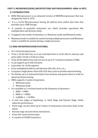
  • 1. UNIT-5: MICROPROCESSOR (ARCHITECTURE AND PROGRAMMING -8086-16 BIT) 5.1 INTRODUCTION:  8086 Microprocessor is an enhanced version of 8085Microprocessor that was designed by Intel in 1976.  It is a 16-bit Microprocessor having 20 address lines and16 data lines that provides up to 1MB storage.  It consists of powerful instruction set, which provides operations like multiplication and division easily.  It supports two modes of operation, i.e. Maximum mode and Minimum mode.  Maximum mode is suitable for system having multiple processors and Minimum mode is suitable for system having a single processor. 5.2 8086 MICROPROCESSOR FEATURES:  It is 16-bit microprocessor  It has a 16-bit data bus, so it can read data from or write data to memory and ports either 16-bit or 8-bit at a time.  It has 20 bit address bus and can access up to 220 memory locations (1MB).  It can support up to 64K I/O ports  It provides 14, 16-bit registers  It has multiplexed address and data bus AD0-AD15 & A16-A19  It requires single phase clock with 33% duty cycle to provide internal timing.  Pre fetches up to 6 instruction bytes from memory and queues them in order to speed up theprocessing.  8086 supports 2 modes of operation 1. Minimum mode 2. Maximum mode  It is available in 3 versions based on the frequency of operation − 1. 8086 → 5MHz 2. 8086-2 → 8MHz 3. (c)8086-1 → 10 MHz  It uses two stages of pipelining, i.e. fetch Stage and Execute Stage, which improves performance.  Fetch stage can pre fetch up to 6 bytes of instructions and stores them in the queue.  Execute stage executes these instructions.  It has 256 vectored interrupts.  It consists of 29,000 transistors.
  • 2. 5.3 REGISTER ORGANIZATION:  8086 has a powerful set of registers known as general purpose registers and special purposeregisters.  All of them are 16-bit registers.  General purpose registers:  These registers can be used as either 8-bit registers or 16-bit registers.  They may be either used for holding data, variables and intermediate results temporarily or for other purposes like a counter or for storing offset address for some particular addressing modes etc.  Special purpose registers:  These registers are used as segment registers, pointers, index registers or as offset storage registers for particular addressing modes.  The 8086 registers are classified into the following types:  General Data Registers  Segment Registers  Pointers and Index Registers  Flag Register 1. General Data Registers:  The registers AX, BX, CX and DX are the general purpose 16-bit registers.  AX is used as 16-bit accumulator. The lower 8-bit is designated as AL and higher 8-bit is designated as AH.  AL Can be used as an 8-bit accumulator for 8-bit operation.  All data register can be used as either 16 bit or 8 bit. BX is a 16 bit register, but BL indicates the lower 8-bitof BX and BH indicates the higher 8-bit of BX.  The register BX is used as offset storage for forming physical address in case of certain addressing modes.  The register CX is used default counter in case of string and loop instructions.  DX register is a general purpose register which may be used as an implicit operand or destination in case of a few instructions.
  • 3. 2. Segment Registers:  There are 4 segment registers. They are:  Code Segment Register(CS)  Data Segment Register(DS)  Extra Segment Register(ES)  Stack Segment Register(SS)  The 8086 architecture uses the concept of segmented memory. 8086 able to address a memory capacity of 1 megabyte and it is byte organized. This 1 megabyte memory is divided into 16 logical segments. Each segment contains 64 Kbytes of memory.  Code segment register (CS): It is used for addressing memory location in the code segment of the memory, where the executable program is stored.  Data segment register (DS): It points to the data segment of the memory where the data is stored.  Extra Segment Register (ES) : It also refers to a segment in the memory which is another data segment in the memory.  Stack Segment Register (SS):  It is used for addressing stack segment of the memory. The stack segment is that segment of memory which is used to store stack data.  While addressing any location in the memory bank, the physical address is calculated from two parts: Physical address= segment address + offset address  The first is segment address, the segment registers contain 16-bit segment base addresses, related to different segment.  The second part is the offset value in that segment. 3. Pointers and Index Registers:  The index and pointer registers are given below:  IP—Instruction pointer-store memory location of next instruction to be executed  BP—Base pointer  SP—Stack pointer  SI—Source index  DI—Destination index  The pointers registers contain offset within the particular segments.  The pointer register IP contains offset within the code segment.  The pointer register BP contains offset within the data segment.  Thee pointer register SP contains offset within the stack segment.
  • 4.  The index registers are used as general purpose registers as well as for offset storage in case of indexed, base indexed and relative base indexed addressing modes.  The register SI is used to store the offset of source data in data segment.  The register DI is used to store the offset of destination in data or extra segment.  The index registers are particularly useful for string manipulation. 4. 8086 flag register and its functions:  The 8086 flag register contents indicate the results of computation in the ALU. It also contains some flag bits to control the CPU operations.  A 16 bit flag register is used in 8086. It is divided into two parts.  Condition code or status flags  Machine control flags  The condition code flag register is the lower byte of the 16-bit flag register. The condition code flag register is identical to 8085 flag register, with an additional overflow flag.  The control flag register is the higher byte of the flag register. It contains three flags namely direction flag (D), interrupt flag (I) and trap flag (T). Flag register configuration
  • 5. The description of each flag bit is as follows: SF (Sign Flag): This flag is set, when the result of any computation is negative. For signed computations the sign flag equals the MSB of the result. ZF (Zero Flag): This flag is set, if the result of the computation or comparison performed by the previous instruction is zero. PF (Parity Flag): This flag is set to 1, if the lower byte of the result contains even number of 1’s. CF (Carry Flag): This flag is set, when there is a carry out of MSB in case of addition or a borrow in case of subtraction. AF (Auxiliary Carry Flag): This is set, if there is a carry from the lowest nibble, i.e., bit three during addition, or borrow for the lowest nibble, i.e., bit three, during subtraction. OF (Over flow Flag): This flag is set, if an overflow occurs, i.e., if the result of a signed operation is large enough to accommodate in a destination register. The result is of more than 7-bits in size in case of 8-bit signed operation and more than 15-bits in size in case of 16-bit sign operations, and then the overflow will be set. TF (Tarp Flag): If this flag is set, the processor enters the single step execution mode. The processor executes the current instruction and the control is transferred to the Trap interrupt service routine. IF (Interrupt Flag): If this flag is set, the mask able interrupts are recognized by the CPU, otherwise they are ignored. D (Direction Flag): This is used by string manipulation instructions. If this flag bit is ‘0’, the string is processed beginning from the lowest address to the highest address, i.e., auto incrementing mode. Otherwise, the string is processed from the highest address towards the lowest address, i.e., auto decrementing mode.
  • 6. 5.4 ARCHITECTURE OF 8086 MICROPROCESSOR:  As shown in the below figure, the 8086 CPU is divided into two independent functional parts  Bus Interface Unit(BIU)  Execution Unit(EU) Dividing the work between these two units’ speeds up processing. The Execution Unit (EU):  The execution unit of the 8086 tells the BIU where to fetch instructions or data from, decodes instructions, and executes instructions.  The EU contains control circuitry, which directs internal operations.  A decoder in the EU translates instructions fetched from memory into a series of actions, which the EU carries out.  The EU has a 16-bit arithmetic logic unit (ALU) which can add, subtract, AND, OR, XOR, increment, decrement, complement or shift binary numbers.  The main functions of EU are:  Decoding of Instructions  Execution of instructions
  • 7.  Steps:  EU extracts instructions from top of queue in BIU  Decode the instructions  Generates operands if necessary  Passes operands to BIU & requests it to perform read or write bus cycles to memory or I/O  Perform the operation specified by the instruction on operands Or  Execution unit gives instructions to BIU stating from where to fetch the data and then decode and execute those instructions. Its function is to control operations on data using the instruction decoder & ALU. EU has no direct connection with system buses as shown in the above figure, it performs operations over data through BIU. Bus Interface Unit (BIU):  The BIU sends out addresses, fetches instructions from memory, reads data from ports and memory, and writes data to ports and memory.  In simple words, the BIU handles all transfers of data and addresses on the buses for the execution unit. Or  BIU takes care of all data and addresses transfers on the buses for the EU like sending addresses, fetching instructions from the memory, reading data from the ports and the memory as well as writing data to the ports and the memory.  EU has no direction connection with System Buses so this is possible with the BIU. EU and BIU are connected with the Internal Bus. 8086 HAS PIPELINING ARCHITECTURE:  While the EU is decoding an instruction or executing an instruction, which does not require use of the buses, the BIU fetches up to six instruction bytes for the following instructions.  The BIU stores these pre-fetched bytes in a first-in-first-out register set called a queue.  When the EU is ready for its next instruction from the queue in the BIU. This is much faster than sending out an address to the system memory and waiting for memory to send back the next instruction byte orbytes.  Except in the case of JMP and CALL instructions, where the queue must be dumped and then reloaded starting from a new address, this pre-fetch and queue scheme greatly speeds up processing.  Fetching the next instruction while the current instruction executes is called pipelining.
  • 8. 5.5 PIN DIAGRAM OF 8086: Intel 8086 is a 16-bit HMOS microprocessor. It is available in 40 pin DIP chip. It uses a 5V DC supply for its operation. The 8086 uses 20-line address bus. It has a 16-line data bus. The 20 lines of the address bus operate in multiplexed mode. The 16-low order address bus lines have been multiplexed with data and 4 high-order address bus lines have been multiplexed with status signals. AD0-AD15: Address/Data bus. These are low order address bus. They are multiplexed with data. When AD lines are used to transmit memory address the symbol A is used instead of AD, for example A0-A15. When data are transmitted over AD lines the symbol D is used in place of AD, for example D0-D7, D8-D15 or D0-D15. A16-A19: High order address bus. These are multiplexed with status signals. S2, S1, S0: Status pins. These pins are active during T4, T1 and T2 states and is returned to passive state (1, 1, 1 during T3 or Tw (when ready is inactive). These are used by the 8288 bus controller for generating all the memory and I/O operation) access control signals. Any change in S2, S1, and S0 during T4 indicates the beginning of a bus cycle. S2 S1 S0 Characteristics 0 0 0 Interrupt acknowledge 0 0 1 Read I/O port
  • 9. 0 1 0 Write I/O port 0 1 1 Halt 1 0 0 Code access1 0 1 Read memory 1 1 0 Write memory 1 1 1 Passive State A16/S3, A17/S4, A18/S5, A19/S6:  The specified address lines are multiplexed with corresponding status signals.  These are the 4 address/status buses. During the first clock cycle, it carries 4- bit address and later it carries status signals. BHE’/S7:  Bus High Enable/Status. During T1 it is low. It is used to enable data onto the most significant half of data bus, D8-D15.  8-bit device connected to upper half of the data bus use BHE (Active Low) signal.  It is multiplexed with status signal S7.  S7 signal is available during T2, T3 and T4. RD’: This is used for read operation. It is an output signal. It is active when low. READY: This is the acknowledgement from the memory or slow device that they have completed the data transfer. The signal made available by the devices is synchronized by the 8284A clock generator to provide ready input to the microprocessor. The signal is active high (1). INTR: Interrupt Request. This is triggered input. This is sampled during the last clock cycles of each instruction for determining the availability of the request. If any interrupt request is found pending, the processor enters the interrupt acknowledge cycle. This can be internally masked after resulting the interrupt enable flag. This signal is active high (1) and has been synchronized internally. NMI: Non maskable interrupt. This is an edge triggered input which results in a type II interrupt. A subroutine is then vectored through an interrupt vector lookup table which is located in the system memory. NMI is non-maskable internally by software. A transition made from low (0) to high (1) initiates the interrupt at the end of the current instruction. This input has been synchronized internally.
  • 10. INTA: Interrupt acknowledge. It is active low (0) during T2, T3 and Tw of each interrupt acknowledge cycle. MN/MX’: Minimum/Maximum. This pin signal indicates what mode the processor will operate in. RQ’/GT1′, RQ’/GT0′: These are the Request/Grant signals used by the other processors requesting the CPU to release the system bus. When the signal is received by CPU, then it sends acknowledgment. RQ/GT0 has a higher priority than RQ/GT1. LOCK’:  It’s an active low pin. It indicates that other system bus masters have not been allowed to gain control of the system bus while LOCK’ is active low (0). The LOCK signal will be active until the completion of the next instruction.  When this signal is active, it indicates to the other processors not to ask the CPU to leave the system bus. It is activated using the LOCK prefix on any instruction RESET: This pin requires the microprocessor to terminate its present activity immediately. The signal must be active high (1) for at least four clock cycles. TEST’: This examined by a ‘WAIT’ instruction. If the TEST pin goes low (0), execution will continue, else the processor remains in an idle state. The input is internally synchronized during each of the clock cycle on leading edge of the clock. CLK:  Clock Input. The clock input provides the basic timing for processing operation and bus control activity. It’s an asymmetric square wave with a 33% duty cycle. Vcc: Power Supply (+5V D.C.) GND: Ground QS1, QS0: Queue Status. These signals indicate the status of the internal 8086 instruction queue according to the table shown below
  • 11. QS0 QS1 Status 0 0 No operation 0 1 First byte of opcode from the queue 1 0 Empty the queue 1 1 Subsequent byte from the queue DT/R: Data Transmit/Receive. This pin is required in minimum systems that want to use an 8286 or 8287 data bus transceiver. The direction of data flow is controlled through the transceiver. DEN: Data enable. This pin is provided as an output enable for the 8286/8287 in a minimum system which uses transceiver. DEN is active low (0) during each memory and input-output access and for INTA cycles. HOLD/HOLDA: HOLD indicates that another master has been requesting a local bus .This is an active high (1). The microprocessor receiving the HOLD request will issue HLDA (high) as an acknowledgement in the middle of a T4 or T1 clock cycle. ALE: Address Latch Enable. ALE is provided by the microprocessor to latch the address into the 8282 or 8283 address latch. It is an active high (1) pulse during T1 of any bus cycle. ALE signal is never floated, is always integer. 5.6 GENERAL BUS OPERATION OF 8086:  The 8086 has a combined address and data bus commonly referred as a time multiplexed address and data bus.  The main reason behind multiplexing address and data over the same pins is the maximum utilization of processor pins and it facilitates the use of 40 pin standard DIP package.  The bus can be de multiplexed using a few latches and transceivers, whenever required.  Basically, all the processor bus cycles consist of at least four clock cycles. These are referred to as T1, T2, T3, and T4. The address is transmitted by the processor during T1. It is present on the bus only for one cycle.  The negative edge of this ALE pulse is used to separate the address and the data or
  • 12. status information. In maximum mode, the status lines S0, S1 and S2 are used to indicate the type of operation.  Status bits S3 to S7 are multiplexed with higher order address bits and the BHE signal. Address is valid during T1 while status bits S3 to S7 are valid during T2 through T4. Maximum mode  In the maximum mode, the 8086 is operated by strapping the MN/MX pin to ground.  In this mode, the processor derives the status signal S2, S1, S0. Another chip called bus controller derives the control signal using this status information.  In the maximum mode, there may be more than one microprocessor in the system configuration. Minimum mode  In a minimum mode 8086 system, the microprocessor 8086 is operated in minimum mode by strapping its MN/MX pin to logic 1.  In this mode, all the control signals are given out by the microprocessor chip itself.  There is a single microprocessor in the minimum mode system.
  • 13. 5.7 8086 MEMORY ORGANIZATION:  Segmented Memory Two types of memory organization are used:  Linear addressing where the entire memory is available to the processor at all the times (Motorola 68000 family).  Segmented addressing where the memory space is divided into several segments and the processor is limited to access program instructions and data in specific segments.  8086 Memory Organization Each memory location 8086 is a byte while the 8086 is a 16-bits microprocessor. Memory Segmentation:  The memory in an 8086 based system is organized as segmented memory.  The CPU 8086 is able to access 1MB of physical memory. The complete 1MB of memory can be divided into 16 segments, each of 64KB size and is addressed by one of the segment register.  The 16-bit contents of the segment register actually point to the starting location of a particular segment. The address of the segments may be assigned as 0000H to F000h respectively.  To address a specific memory location within a segment, we need an offset address. The offset address values are from 0000H to FFFFH so that the physical addresses range from 00000H to FFFFFH. Advantages of the segmented memory scheme are as follows:  Allows the memory capacity to be 1MB although the actual addresses to be handled are of 16-bitsize.  Allows the placing of code, data and stack portions of the same program in different parts (segments) of memory, for data and code protection.  Permits a program and/or its data to be put into different areas of memory each time the program is executed, i.e., provision for relocation is done. Overlapping and Non-overlapping Memory segments:  In the overlapping area locations physical address = CS1+IP1 = CS2+IP2. Where ‘+’ indicates the procedure of physical address formation.
  • 14. 5.8 MINIMUM MODE & TIMINGS: Minimum Mode 8086 System:  The microprocessor 8086 is operated in minimum mode by strapping its MN/MX pin to logic 1.  In this mode, all the control signals are given out by the microprocessor chip itself. There is a single microprocessor in the minimum mode system.  The remaining components in the system are latches, transreceivers, clock generator, memory and I/O devices.  Some type of chip selection logic may be required for selecting memory or I/O devices, depending upon the address map of the system  Latches are generally buffered output D-type flip-flops like 74LS373 or 8282. They are used for separating the valid address from the multiplexed address/data signals and are controlled by the ALE signal generated by 8086. Minimum Mode Configuration for 8086
  • 15.  Since it has 20 address lines and 16 data lines, the 8086 CPU requires three octal address latches and two octal data buffers for the complete address and data separation.  Transceivers are the bidirectional buffers and sometimes they are called as data amplifiers. They are required to separate the valid data from the time multiplexed address/data signal.  They are controlled by two signals, namely, DEN’ and DT/R’. The DEN’ signal indicates that the valid data is available on the data bus, while DT/R’ indicates the direction of data, i.e. from or to theprocessor.  The system contains memory for the monitor and users program storage. Usually, EPROMS are used for monitor storage, while RAMs for users program storage.  A system may contain I/O devices for communication with the processor as well as some special purpose I/O devices.  The clock generator generates the clock from the crystal oscillator and then shapes it and divides to make it more precise so that it can be used as an accurate timing reference for the system.  The clock generator also synchronizes some external signals with the systemclock.  The working of the minimum mode configuration system can be better described in terms of the timing diagrams rather than qualitatively describing the operations.  The opcode fetch and read cycles are similar. Hence the timing diagram can be categorized in two parts, the first is the timing diagram for read cycle and the second is the timing diagram for write cycle. Timing Diagrams:  Timing diagram is graphical representation of the operations of microprocessor with respect to the time.  State: one cycle of the clock is called state.  Machine cycle: The basic microprocessor operation such as reading a byte from memory or writing a byte to a port is called machine cycle and made up of more than onestate.  Instruction cycle: The time required for microprocessor to fetch and execute an entire instruction is called Instruction cycle and made up of more than one machine cycle. Note: An instruction cycle is made up of machine cycles, and a machine cycle is made up of states. The time for a state is determined by the frequency of the clock signal.
  • 16. Read cycle timing diagram for Minimum mode:  The best way to analyze a timing diagram such as the one to think of time as a vertical line moving from left to right across the diagram.  The read cycle begins in T1 with the assertion of the address latch enable (ALE) signal and also M/IO’signal.  During the negative going edge of this signal, the valid address is latched on the local bus. The BHE’ and A0 signals address low, high or both bytes.  From T1 to T4, the M/IO’ signal indicate a memory or I/O operation. At T2, the address is removed from the local bus and is sent to the output. The bus is then tristated. The read (RD’) control signal is also activated in T2.  The read (RD’) signal causes the addressed device to enable its data bus driver. After goes low, the valid data is available on the data bus. The addressed device will drive the READY line high. When the processor returns the read signal to high level, the addressed device will again tristate its bus drivers.
  • 17. Write cycle timing diagram for Minimum mode:  A write cycle also begins with the assertion of ALE and the emission of the address. The M/IO’ signal is again asserted to indicate a memory or I/O operation.  In T2, after sending the address in T1, the processor sends the data to be written to the addressed location. The data remains on the bus until middle of T4 state. The WR’ becomes active at the beginning of T2 (unlike RD’ is somewhat delayed in T2 to provide time for floating).  The BHE’ and A0 signals are used to select the proper byte or bytes of memory or I/O word to be reador written.  The M/IO’, RD’ and WR’ signals indicate the types of data transfer as specified in Table.
  • 18. 5.9 MAXIMUM MODE &TIMINGS  In the maximum mode, the 8086 is operated by strapping the MN/MX’ pin to ground. In this mode, the processor derives the status signals S2’, S1’ and S0’. Another chip called bus controller derives the control signals using this status information.  In the maximum mode, there may be more than one microprocessor in the system configuration. The other components in the system are the same as in the minimum mode system. The general system organization is as shown in the below figure. The basic functions of the bus controller chip IC8288, is to derive control signals like RD’ and WR’ (for memory and I/O devices), DEN, DT/R’, ALE, etc. using the information made available by the processor on the status lines.  The bus controller chip has input lines S2’, S1’ and S0’ and CLK. These inputs to 8288 are driven by the CPU. It derives the outputs ALE, DEN, DT/R’, MWTC’, MRDC’, IORC’, IOWC’ and INTA’.  INTA’ pin is used to issue two interrupt acknowledge pulses to the interrupt controller or to an interrupting device.  IORC*, IOWC* are I/O read command and I/O write command signals respectively. These signals enable an IO interface to read or write the data from or to the addressed port. The MRDC*, MWTC* are memory read command and memory write command signals respectively and may be used as memory read and write signals. All these command signals instruct the memory to accept or send data from or to thebus.  The maximum mode system timing diagrams are also divided in two portions as read (input) and write (output) timing diagrams. The address/data and address/status timings are similar to the minimum mode. ALE is asserted in T1, just like minimum mode. The only difference lies in the status signals used and the available control and advanced command signals.
  • 19. Read cycle timing diagram for Maximum mode:
  • 20. Write cycle timing diagram for Maximum mode: 5.10 INTERRUPTS: Definition: The meaning of „interrupts‟ is to break the sequence of operation. While the CPU is executing a program, on „interrupt‟ breaks the normal sequence of execution of instructions, diverts its execution to some other program called Interrupt Service Routine (ISR).After executing ISR , the control is transferred back again to the main program. Interrupt processing is an alternative to polling. Or Interrupt is the method of creating a temporary halt during program execution and allows peripheral devices to access the microprocessor. The microprocessor responds to that interrupt with an ISR (Interrupt Service Routine), which is a short program to instruct the microprocessor on how to handle the interrupt. The following image shows the types of interrupts we have in a 8086 microprocessor −
  • 21. Need for Interrupt: Interrupts are particularly useful when interfacing I/O devices that provide or require data at relatively low data transfer rate. Types of Interrupts: There are two types of Interrupts in 8086. 1. Hardware Interrupts 2. Software Interrupts HARDWARE INTERRUPTS:  Hardware interrupt is caused by any peripheral device by sending a signal through a specified pin to the microprocessor.  The 8086 has two hardware interrupt pins, i.e. NMI and INTR. NMI is a non- maskable interrupt and INTR is a maskable interrupt having lower priority. One more interrupt pin associated is INTA called interrupt acknowledge. NMI (non-maskable): It is a single non-maskable interrupt pin (NMI) having higher priority than the maskable interrupt request pin (INTR) and it is of type 2 interrupt. When this interrupt is activated, these actions take place: −  Completes the current instruction that is in progress.  Pushes the Flag register values on to the stack.  Pushes the CS (code segment) value and IP (instruction pointer) value of the return address on to the stack.  IP is loaded from the contents of the word location 00008H.  CS is loaded from the contents of the next word location 0000AH.  Interrupt flag and trap flag are reset to 0. INTR (Maskable):  The INTR is a maskable interrupt because the microprocessor will be interrupted only if interrupts are enabled using set interrupt flag instruction. It should not be enabled using clear interrupt Flag instruction.  The INTR interrupt is activated by an I/O port. If the interrupt is enabled and NMI is disabled, then the microprocessor first completes the current execution and sends ‘0’ on INTA pin twice. The first ‘0’ means INTA informs the external device to get ready and during the second ‘0’ the microprocessor receives the 8 bit, say X, from the programmable interrupt controller. These actions are taken by the microprocessor: −  First completes the current instruction.  Activates INTA output and receives the interrupt type, say X.  Flag register value, CS value of the return address and IP value of the return address are pushed on to the stack.
  • 22.  IP value is loaded from the contents of word location X × 4  CS is loaded from the contents of the next word location.  Interrupt flag and trap flag is reset to 0 SOFTWARE INTERRUPTS:  Some instructions are inserted at the desired position into the program to create interrupts. These interrupt instructions can be used to test the working of various interrupt handlers. It includes: − INT- Interrupt instruction with type number  It is 2-byte instruction. First byte provides the op-code and the second byte provides the interrupt type number. There are 256 interrupt types under this group. Its execution includes the following steps: −  Flag register value is pushed on to the stack.  CS value of the return address and IP value of the return address are pushed on to the stack.  IP is loaded from the contents of the word location ‘type number’ × 4  CS is loaded from the contents of the next word location.  Interrupt Flag and Trap Flag are reset to 0  The starting address for type0 interrupt is 000000H, for type1 interrupt is 00004H similarly for type2 is 00008H and ……so on. The first five pointers are dedicated interrupt pointers. i.e. −  TYPE 0 interrupt represents division by zero situation.  TYPE 1 interrupt represents single-step execution during the debugging of a program.  TYPE 2 interrupt represents non-maskable NMI interrupt.  TYPE 3 interrupt represents break-point interrupt.  TYPE 4 interrupt represents overflow interrupt.  The interrupts from Type 5 to Type 31 are reserved for other advanced microprocessors, and interrupts from 32 to Type 255 are available for hardware and software interrupts. INT 3-Break Point Interrupt Instruction  It is a 1-byte instruction having op-code is CCH. These instructions are inserted into the program so that when the processor reaches there, then it
  • 23. stops the normal execution of program and follows the break-point procedure. Its execution includes the following steps: −  Flag register value is pushed on to the stack.  CS value of the return address and IP value of the return address are pushed on to the stack.  IP is loaded from the contents of the word location 3×4 = 0000CH  CS is loaded from the contents of the next word location.  Interrupt Flag and Trap Flag are reset to 0 INTO - Interrupt on overflow instruction  It is a 1-byte instruction and their mnemonic INTO. The op-code for this instruction is CEH. As the name suggests it is a conditional interrupt instruction, i.e. it is active only when the overflow flag is set to 1 and branches to the interrupt handler whose interrupt type number is 4. If the overflow flag is reset then, the execution continues to the next instruction. Its execution includes the following steps: −  Flag register values are pushed on to the stack.  CS value of the return address and IP value of the return address are pushed on to the stack.  IP is loaded from the contents of word location 4×4 = 00010H  CS is loaded from the contents of the next word location.  Interrupt flag and Trap flag are reset to 0 5.11 ADDRESSING MODES: The way of specifying data to be operated by an instruction is known as addressing modes. This specifies that the given data is an immediate data or an address. It also specifies whether the given operand is register or register pair. 1. Immediate addressing mode:  The addressing mode in which the data operand is a part of the instruction itself is known as immediate addressing mode.  Example 2. Register mode:  In this type of addressing mode both the operands are registers. Or  It means that the register is the source of an operand for an instruction.
  • 24.  Example:  MOV CX, AX ; copies the contents of the 16-bit AX register into the 16-bit CX register  ADD BX, AX 3. Displacement or direct mode:  In this type of addressing mode the effective address is directly given in the instruction as displacement.  Example:  MOV AX, [DISP]  MOV AX, [0500] 4. Register indirect addressing mode:  This addressing mode allows data to be addressed at any memory location through an offset address held in any of the following registers: BP, BX, DI & SI.  Example  MOV AX, [BX] ; Suppose the register BX contains 4895H, then the contents 4895H are moved to AX  ADD CX, [BX]  ADD AL, [BX] 5. Based addressing mode:  In this addressing mode, the offset address of the operand is given by the sum of contents of the BX/BP registers and 8-bit/16-bit displacement.  Example:  MOV DX,[BX+04]  ADD CL, [BX+08] 6. Indexed addressing mode:  In this addressing mode, the operands offset address is found by adding the contents of SI (Index register) or DI (displacement) register and 8-bit/16- bit displacements. Example:  MOV BX, [SI+16]  ADD AL, [DI+16] 7. Based-index addressing mode:  In this addressing mode, the offset address of the operand is computed by summing the base register (BX or BP) to the contents of an Index register (SI or DI).
  • 25.  Offset= [BX or BP]+[SI or DI]  BX is used as a base register for data segment, and BP is used as a base register for stack segment.  Example:  ADD AX, [BX+SI]  MOV CX,[BX+SI]  MOV AX,[AX+DI] 8. Based indexed with displacement mode:  In this type of addressing mode the effective address is the sum of index register, base register and displacement.  Offset= [BX+BP] + [SI or DI] +8-bit or 16-bit displacement.  Example:  MOV AX, [BX+SI+05] an example of 8-bit displacement.  MOV AX, [BX+SI+1235H] an example of 16-bit displacement.  MOV AL, [SI+BP+2000] 5.12 INSTRUNCTION SET: The 8086 instructions are categorized into the following main types  Data transfer instructions  Arithmetic instructions  Program control transfer instructions  Machine control instructions  Shift/rotate instructions  Flag manipulation instructions  String instructions 1. DATA COPY /TRANSFER INSTRUCTIONS:  These type of instructions are used to transfer data from source operand to destination operand. All the store, load, move, exchange input and output instructions belong to this category. MOV instruction  It is a general purpose instruction to transfer byte or word from register to register, memory to register, register to memory or with immediate addressing  MOV destination, source  Here the source and destination needs to be of the same size that is both 8-bit and both 16-bit.  MOV instruction does not affect any flags.
  • 26. MOV BX, 00F2H ; load the immediate number 00F2H in BX Register MOV CL, [2000H] ; Copy the 8 bit content of the memory Location, at a displacement of 2000H from data segment base to the CL register MOV [589H], BX ; Copy the 16 bit content of BX register on to the memory location, which at a displacement of 589H from the data segment base. MOV DS, CX ; Move the content of CX to DS PUSH instruction:  The PUSH instruction decrements the stack pointer by two and copies the word from source to the location where stack pointer now points. Here the source must of word size data. Source can be a general purpose register, segment register or a memory location.  The PUSH instruction first pushes the most significant byte to sp-1, then the least significant to the sp-2.  Push instruction does not affect any flags.  Example:-  PUSH CX ; Decrements SP by 2, copy content of CX to the stack (figure shows execution of this instruction)  PUSH DS ; Decrement SP by 2 and copy DS to stack POPinstruction:  The POP instruction copies a word from the stack location pointed by the stack pointer to the destination. The destination can be a General purpose register, a segment register or a memory location. Here after the content is copied the stack pointer is automatically incremented bytwo.  The execution pattern is similar to that of the PUSH instruction.  Example:  POP CX; Copy a word from the top of the stack to CX and increment SP by2. IN & OUT instructions The IN instruction will copy data from a port to the accumulator. If 8 bit is read the data will go to AL and if 16 bit then to AX. Similarly OUT instruction is used to
  • 27. copy data from accumulator to an output port. Both IN and OUT instructions can be done using direct and indirect addressing modes.  Example:  IN AL, 0F8H ; Copy a byte from the port 0F8H to AL  MOV DX, 30F8H ; Copy port address in DX  IN AL, DX ; Move 8 bit data from 30F8H port  IN AX, DX ; Move 16 bit data from 30F8H port  OUT 047H, AL ; Copy contents of AL to 8 bit port 047H  MOV DX, 330F8H ; Copy port address in DX  OUT DX, AL ; Move 8 bit data to the 30F8H port  OUT DX, AX ; Move 16 bit data to the 30F8H port XCHG instruction  The XCHG instruction exchanges contents of the destination and source. Here destination and source can be register and register or register and memory location, but XCHG cannot interchange the value of 2 memory locations.  XCHG Destination, Source  Example:  XCHG BX, CX ; exchange word in CX with the word in BX  XCHG AL, CL ; exchange byte in CL with the byte in AL  XCHG AX, SUM[BX] ; Here physical address, which is DS +SUM+ [BX]. The content at physical address and the content of AX are interchanged 2. Arithmetic and Logical instructions: All the instructions performing arithmetic, logical, increment, decrement, compare and ASCII instructions belong to this category. ADD instruction:  Add instruction is used to add the current contents of destination with that of source and store the result in destination. Here we can use register and/or memory locations.  AF, CF, OF, PF, SF, and ZF flags are affected.
  • 28.  ADD Destination, Source  Example: o ADD AL, 0FH ; Add the immediate content, 0FH to the content of AL and store the result in AL o ADD AX, BX ; AX <= AX+BX o ADD AX,0100H – IMMEDIATE o ADD AX,BX – REGISTER o ADD AX,[SI] – REGISTER INDIRECT OR INDEXED o ADD AX, [5000H] – DIRECT o ADD [5000H], 0100H – IMMEDIATE o ADD 0100H – DESTINATION AX (IMPLICT) ADC: ADD WITH CARRY This instruction performs the same operation as ADD instruction, but adds the carry flag bit (which may be set as a result of the previous calculation) to the result. All the condition code flags are affected by this instruction. The examples of this instruction along with the modes are as follows: Example: o ADC AX,BX – REGISTER o ADC AX,[SI] – REGISTER INDIRECT OR INDEXED o ADC AX, [5000H] – DIRECT o ADC [5000H], 0100H – IMMEDIATE o ADC 0100H – IMMEDIATE (AX IMPLICT) SUB instruction:  SUB instruction is used to subtract the current contents of destination with that of source and store the result in destination. Here we can use register and/or memory locations. AF, CF, OF, PF, SF, and ZF flags are affected  SUB Destination, Source  Example: o SUB AL, 0FH ; subtract the immediate content, 0FH from the content of AL and store the result in AL o SUB AX, BX ; AX <= AX-BX o SUB AX,0100H – IMMEDIATE (DESTINATION AX) o SUB AX,BX – REGISTER o SUB AX,[5000H] – DIRECT o SUB [5000H], 0100H – IMMEDIATE SBB: SUBTRACT WITH BORROW:
  • 29.  To subtract with borrow instruction subtracts the source operand and the borrow flag (CF) which may reflect the result of the previous calculations, from the destination operand. Subtraction with borrow, here means subtracting 1 from the subtraction obtained by SUB, if carry (borrow) flag is set.  The result is stored in the destination operand. All the flags are affected (condition code) by this instruction. The examples of this instruction are as follows:  Example:  SBB AX, 0100H – IMMEDIATE (DESTINATION AX)  SBB AX, BX – REGISTER  SBB AX,[5000H] – DIRECT  SBB [5000H], 0100H – IMMEDIATE CMP: COMPARE:  The instruction compares the source operand, which may be a register or an immediate data or a memory location, with a destination operand that may be a register or a memory location.  For comparison, it subtracts the source operand from the destination operand but does not store the result anywhere. The flags are affected depending upon the result of the subtraction.  If both of the operands are equal, zero flag is set. If the source operand is greater than the destination operand, carry flag is set or else, carry flag is reset. The examples of this instruction are as follows:  Example:  CMP BX, 0100H –IMMEDIATE  CMP AX, 0100H –IMMEDIATE  CMP [5000H], 0100H – DIRECT  CMP BX,[SI] – REGISTER INDIRECT OR INDEXED  CMP BX, CX – REGISTER INC & DEC instructions: 1. INC and DEC instructions are used to increment and decrement the content of the specified destination by one. AF, CF, OF, PF, SF, and ZF flags are affected. 2. Example: INC AL ; ALAL + 1 INC AX ; AXAX + 1
  • 30. DEC AL ; AL AL – 1 DEC AX ; AXAX – 1 AND instruction:  This instruction logically ANDs each bit of the source byte/word with the corresponding bit in the destination and stores the result in destination. The source can be an immediate number, register or memory location, register can be a register or memory location.  The CF and OF flags are both made zero, PF, ZF, SF are affected by the operation and AF is undefined.  AND Destination, Source  Example:  AND BL, AL; suppose BL=1000 0110 and AL = 1100 1010 then after the operation BL would be BL= 1000 0010.  AND CX, AX; CX  CX AND AX  AND CL, 08; CL CL AND (0000 1000) OR instruction:  This instruction logically ORs each bit of the source byte/word with the corresponding bit in the destination and stores the result in destination. The source can be an immediate number, register or memory location, register can be a register or memory location.  The CF and OF flags are both made zero, PF, ZF, SF are affected by the operation and AF is undefined.  OR Destination, Source  Example:  OR BL, AL ; suppose BL=1000 0110 and AL = 1100 1010 then after the operation BL would be BL= 1100 1110.  OR CX, AX ; CXAX AND AX  OR CL, 08 ; CLCL AND (0000 1000) NOT instruction:  The NOT instruction complements (inverts) the contents of an operand register or a memory location, bit by bit. The examples are asfollows: 1. Example: 2. NOT AX (BEFORE AX= (1011)2= (B) 16 AFTER EXECUTION AX= (0100)2= (4)16). 3. NOT [5000H] XOR instruction:  The XOR operation is again carried out in a similar way to the AND and OR
  • 31. operation. The constraints on the operands are also similar. The XOR operation gives a high output, when the 2 input bits are dissimilar. Otherwise, the output is zero. The example instructions are as follows:  Example:  XOR AX, 0098H  XOR AX, BX  XOR AX, [5000H] 3. Shift / Rotate Instructions: 1) Shift instructions move the binary data to the left or right by shifting them within the register or memory location. They also can perform multiplication of powers of 2+n and division of powers of2-n. 2) There are two type of shifts logical shifting and arithmetic shifting, later is used with signed numbers while former with unsigned. SHL/SAL instruction:  Both the instruction shifts each bit to left, and places the MSB in CF and LSB is made 0. The destination can be of byte size or of word size, also it can be a register or a memory location. Number of shifts is indicated by thecount.  All flags are affected.  SAL/SHL destination, count Example: MOV BL, B7H ; BL is made B7H SAL BL, 1 ; Shift the content of BL register one place to left. Before Execution, CY B7 B6 B5 B4 B3 B2 B1 B0 0 1 0 1 1 0 1 1 1 After Execution, CY B7 B6 B5 B4 B3 B2 B1 B0 1 0 1 1 0 1 1 1 0 SHR instruction:  This instruction shifts each bit in the specified destination to the right and 0
  • 32. is stored in the MSB position. The LSB is shifted into the carry flag. The destination can be of byte size or of word size, also it can be a register or a memory location. Numberof shifts is indicated by the count.  All flags are affected  Before execution, B7 B6 B5 B4 B3 B2 B1 B0 CY 10 1 1 0 1 1 1 0  After execution, B7 B6 B5 B4 B3 B 2 B1 B0 CY 0 1 0 1 1 0 1 1 1 ROL instruction:  This instruction rotates all the bits in a specified byte or word to the left some number of bit positions. MSB is placed as a new LSB and a new CF. The destination can be of byte size or of word size, also it can be a register or a memory location. Number of shifts is indicated by the count.  All flags are affected  ROL destination, count Example: MOV BL, B7H ; BL is made B7H ROL BL, 1 ; rotates the content of BL register one place to the left. Before Execution: CY B7 B 6 B B5 B 4 B 3 B 2 B1 B 0 0 1 0 1 1 0 1 1 1 After the execution, CY B7 B6 B5 B4 B3 B2 B1 B0 1 0 1 1 0 1 1 1 1 ROR instruction:  This instruction rotates all the bits in a specified byte or word to the right
  • 33. some number of bit positions. LSB is placed as a new MSB and a new CF. The destination can be of byte size or of word size, also it can be a register or a memory location. Number of shifts is indicated by the count.  All flags are affected.  ROR destination, count  Example: MOV BL, B7H ; BL is made B7H ROR BL, 1 ; shift the content of BL register one place to theright.  Before execution, B7 B6 B5 B4 B3 B2 B1 B0 CY 1 0 1 1 0 1 1 1 0  After execution, B7 B6 B5 B4 B3 B2 B 1 B0 CY 1 1 0 1 1 0 1 1 1 RCR instruction  This instruction rotates all the bits in a specified byte or word to the right some number of bit positions along with the carry flag. LSB is placed in a new CF and previous carry is placed in the new MSB. The destination can be of byte size or of word size, also it can be a register or a memory location. Number of shifts is indicated by the count.  All flags are affected  General Format: RCR destination, count  Example: MOV BL, B7H ; BL is made B7H RCR BL, 1 ; shift the content of BL register one place to the right.  Before execution, B7 B6 B5 B4 B3 B2 B1 B0 CY 1 0 1 1 0 1 1 1 0  After execution, B7 B6 B5 B4 B3 B2 B1
  • 34. B0 CY 0 1 0 1 1 0 1 1 1 4. PROGRAM CONTROL TRANSFER INSTRUCTIONS:  These instructions transfer control of execution to the specified address. All the call, jump, interrupt and return instruction belong to this class.  There are 2 types of such instructions. 1. Unconditional transfer instructions – CALL, RET, JMP 2. Conditional transfer instructions – J condition CALL instruction:  The CALL instruction is used to transfer execution to a subprogram or procedure. There are two types of CALL instructions, near and far.  A near CALL is a call to a procedure which is in the same code segment as the CALL instruction. 8086 when encountered a near call, it decrements the SP by 2 and copies the offset of the next instruction after the CALL on the stack. It loads the IP with the offset of the procedure then to start the execution of the procedure.  A far CALL is the call to a procedure residing in a different segment. Here value of CS and offset of the next instruction both are backed up in the stack. And then branches to the procedure by changing the content of CS with the segment base containing procedure and IP with the offset of the first instruction of the procedure.  Example: Near call CALL PRO ; PRO is the name of the procedure CALL CX ; Here CX contains the offset of the first instruction of the procedure, that is replaces the content IP with the content of CX Far call CALL DWORD PTR [8X]; New values for CS and IP are fetched from four Memory locations in the DS. The new value for CS is fetched from [8X] and [8X+1], the new IP is fetched from [8X+2] and [8X+3]. RET instruction:  RET instruction will return execution from a procedure to the next instruction after the CALL instruction in the calling program. If it was a near call, then IP is replaced with the value at the top of the stack, if it had been a far call, then another POP of the stack is required. This second popped data from the stack is
  • 35. put in the CS, thus resuming the execution of the calling program.  RET instruction does not affect any flags. JMP INSTRUCTION:  This is also called as unconditional jump instruction, because the processor jumps to the specified location rather than the instruction after the JMP instruction. Jumps can be short jumps when the target address is in the same segment as the JMP instruction or far jumps when it is in a different segment. Conditional Jump (J cond)  Conditional jumps are always short jumps in 8086. Here jump is done only if the condition specified is true/false. Ifthe condition is not satisfied, then the execution proceeds in the normal way. Iteration control instructions:  These instructions are used to execute a series of instructions some number of times. The number is specified in the CX register, which will be automatically decremented in course of iteration. But here the destination address for the jump must be in the range of -128 to 127 bytes. Example: LOOP : loop through the set of instructions until CX is 0 LOOPE/LOOPZ : here the set of instructions are repeated until CX=0 or ZF=0 LOOPNE/LOOPNZ: here repeated until CX=0 or ZF=1 5. MACHINE CONTROL INSTRUCTIONS:  These instructions control the machine status. NOP, HLT, WAIT and LOCK instructions belong to this class. HLT instruction  The HLT instruction will cause the 8086 microprocessor to fetching and executing instructions.  The 8086 will enter a halt state. The processor gets out of this Halt signal upon an interrupt signal in INTR pin/NMI pin or a reset signal on RESET input WAIT instruction  When this instruction is executed, the 8086 enters into an idle state. This idle state is continued till a high is received on the TEST input pin or a valid interrupt signal is received. Wait affects no flags. It generally is used to synchronize the 8086 with a peripheral device(s).
  • 36. ESC instruction  This instruction is used to pass instruction to a coprocessor like 8087. There is a 6 bit instruction for the coprocessor embedded in the ESC instruction. In most cases the 8086 treats ESC and a NOP, but in some cases the 8086 will access data items in memory for the coprocessor LOCK instruction  In multiprocessor environments, the different microprocessors share a system bus, which is needed to access external devices like disks. LOCK Instruction is given as prefix in the case when a processor needs exclusive access of the system bus for a particular instruction.  It affects no flags.  LOCK XCHG SEMAPHORE, AL : The XCHG instruction requires two Bus accesses.  The lock prefix prevents another processor from taking control of the system bus between the 2 accesses NOP instruction  At the end of NOP instruction, no operation is done other than the fetching and decoding of the instruction. It takes 3 clock cycles. NOP is used to fill in time delays or to provide space for instructions while trouble shooting. NOP affects no flags. 6. FLAG MANIPULATION INSTRUCTIONS:  All the instructions which directly affect the flag register come under this group of instructions. Instructions like CLD, STD, CLI, STI etc.., belong to this category ofinstructions.  STC instruction This instruction sets the carry flag. It does not affect any other flag.  CLC instruction This instruction resets the carry flag to zero. CLC does not affect any other flag.
  • 37.  CMC instruction This instruction complements the carry flag. CMC does not affect any other flag.  STD instruction This instruction is used to set the direction flag to one so that SI and/or DI can be decremented automatically after execution of string instruction. STD does not affect any other flag.  CLD instruction This instruction is used to reset the direction flag to zero so that SI and/or DI can be incremented automatically after execution of string instruction. CLD does not affect any other flag.  STI instruction This instruction sets the interrupt flag to 1. This enables INTR interrupt of the 8086. STI does not affect any other flag.  CLI instruction This instruction resets the interrupt flag to 0. Due to this the 8086 will not respond to an interrupt signal on its INTR input. CLI does not affect any other flag. 7. STRING MANIPULATION INSTRUCTIONS: These instructions involve various string manipulation operations like Load, move, scan, compare, store etc.  MOVS/MOVSB/MOVSW  These instructions copy a word or byte from a location in the data segment to a location in the extra segment. The offset of the source is in SI and that of destination is in DI. For multiple word/byte transfers the count is stored in the CX register.  When direction flag is 0, SI and DI are incremented and when it is 1, SI and DI are decremented.  MOVS affect no flags. MOVSB is used for byte sized movements while MOVSW is for word sized. Example: CLD ; clear the direction flag to auto increment SI andDI MOV AX, 0000H; MOV DS, AX ; initialize data segment register to 0 MOV ES, AX ; initialize extra segment register to0 MOV SI, 2000H ; Load the offset of the string1 in SI MOV DI, 2400H ; Load the offset of the string2 in DI MOV CX, 04H ; load length of the string in CX
  • 38. REP MOVSB ; decrement CX and MOVSB until CX will be 0  REP/REPE/REP2/REPNE/REPNZ  REP is used with string instruction; it repeats an instruction until the specified condition becomes false. Example: Comments REP CX=0 REPE/REPZ CX=0 OR ZF=0 REPNE/REPNZ CX=0 OR ZF=1  LODS/LODSB/LODSW  This instruction copies a byte from a string location pointed to by SI to AL or a word from a string location pointed to by SI to AX.LODS does not affect any flags. LODSB copies byte and LODSW copies word. Example: CLD ; clear direction flag to auto increment SI MOVSI, OFFSET S_STRING ; point SI at string LODS S_STRING ;  STOS/STOSB/STOSW  The STOS instruction is used to store a byte/word contained in AL/AX to the offset contained in the DI register. STOS does not affect any flags. After copying the content DI is automatically incremented or decremented, based on the value of direction flag. Example:  MOV DL, OFFSET D_STRING; assign DI with destination address.  STOS D_STRING ; assembler uses string name to determine byte or Word, if byte then AL is used and if of word size, AX is used. 5. CMPS/CMPSB/CMPSW  CMPS is used to compare the strings, byte wise or word wise. The comparison is affected by subtraction of content pointed by DI from that pointed by SI. The AF, CF, OF, PF, SF and ZF flags are affected by this instruction, but neither operand is affected.
  • 39. Example: Comments MOV SI, OFFSET STRING_A ; Point first string MOV DI, OFFSET STRING_B ; Point second string MOV CX, 0AH ; Set the counter as 0AH CLD ; Clear direction flag to auto increment REPE CMPSB ; Repeatedly compare till unequal or counter =0 5.13 ASSEMBLER DIRECTIVES AND OPERATOR:  There are some instructions in the assembly language program which are not a part of processor instruction set. These instructions are instructions to the assembler, linker and loader. These are referred to as pseudo-operations or as assembler directives. The assembler directives enable us to control the way in which a program assembles and lists. They act during the assembly of a program and do not generate any executable machine code.  There are many specialized assembler directives. Let us see the commonly used assembler directive in 8086 assembly language programming. ASSUME:  It is used to tell the name of the logical segment the assembler to use for a specified segment.  E.g.: ASSUME CS: CODE tells that the instructions for a program are in a logical segment named CODE. DB -Define Byte:  The DB directive is used to reserve byte or bytes of memory locations in the available memory. While preparing the EXE file, this directive directs the assembler to allocate the specified number of memory bytes to the said data type that may be a constant, variable, string, etc. Another option of this directive also initializes the reserved memory bytes with the ASCII codes of the characters specified as a string. The following examples show how the DB directive is used for different purposes.  RANKS DB 01H, 02H, 03H, 04H This statement directs the assembler to reserve four memory locations for a list named RANKS and initialize them with the above specified four values.
  • 40.  MESSAGE DB„GOOD MORNING‟ This makes the assembler reserve the number of bytes of memory equal to the number of characters in the string named MESSAGE and initializes those locations by the ASCII equivalent of these characters.  VALUE DB 50H This statement directs the assembler to reserve 50H memory bytes and leave them uninitialized for the variable named VALUE. DD:  Define Double word - used to declare a double word type variable or to reserve memory locations that can be accessed as double word. E.g.: ARRAY _POINTER DD 25629261H declares a double word named ARRAY_POINTER. DQ -Define Quad word:  This directive is used to direct the assembler to reserve 4 words (8 bytes) of memory for the specified variable and may initialize it with the specified values. DT -Define Ten Bytes:  The DT directive directs the assembler to define the specified variable requiring 10-bytes for its storage and initialize the 10-bytes with the specified values. The directive may be used in case of variables facing heavy numerical calculations, generally processed by numericalprocessors. DW -Define Word:  The DW directives serves the same purposes as the DB directive, but it now makes the assembler reserve the number of memory words (16-bit) instead of bytes. Some examples are given to explain this directive.  WORDS DW 1234H, 4567H, 78ABH, 045CH This makes the assembler reserve four words in memory (8 bytes), and initialize the words with the specified values in the statements. During initialization, the lower bytes are stored at the lower memory addresses, while the upper bytes are stored at the higher addresses.  NUMBER1 DW 1245H This makes the assembler reserve one word in memory. END-End of Program:  The END directive marks the end of an assembly language program. When the assembler comes across this END directive, it ignores the source lines available
  • 41. later on. Hence, it should be ensured that the END statement should be the last statement in the file and should not appear in between. Also, no useful program statement should lie in the file, after the END statement. ENDP:  End Procedure - Used along with the name of the procedure to indicate the end of a procedure.  E.g.: SQUARE_ROOT PROC: start of procedure SQUARE_ROOT ENDP: End of procedure ENDS-End of Segment:  This directive marks the end of a logical segment. The logical segments are assigned with the names using the ASSUME directive. The names appear with the ENDS directive as prefixes to mark the end of those particular segments. Whatever are the contents of the segments, they should appear in the program before ENDS. Any statement appearing after ENDS will be neglected from the segment. The structure shown below explains the fact more clearly. EQU:  Equate - Used to give a name to some value or symbol. Each time the assembler finds the given name in the program, it will replace the name with the vale.  E.g.: CORRECTION_FACTOR EQU 03H MOV AL, CORRECTION_FACTOR EVEN:  Tells the assembler to increment the location counter to the next even address if it is not already at an even address.  Used because the processor can read even addressed data in one clock cycle EXTRN:  Tells the assembler that the names or labels following the directive are in some other assembly module.  For example if a procedure in a program module assembled at a different time from that which contains the CALL instruction ,this directive is used to tell the assembler that the procedure isexternal GLOBAL:  Can be used in place of a PUBLIC directive or in place of an EXTRN directive.  It is used to make a symbol defined in one module available to other modules.  E.g.: GLOBAL DIVISOR makes the variable DIVISOR public so that it can be accessed from other modules.
  • 42. GROUP:  Used to tell the assembler to group the logical statements named after the directive into one logical group segment, allowing the contents of all the segments to be accessed from the same group segment base.  E.g.: SMALL_SYSTEM GROUP CODE, DATA, STACK_SEG INCLUDE:  Used to tell the assembler to insert a block of source code from the named file into the current source module.  This will shorten the source code. LABEL:  Used to give a name to the current value in the location counter.  This directive is followed by a term that specifies the type you want associated with that name.  E.g: ENTRY_POINT LABEL FAR  NEXT: MOV AL, BL NAME:  Used to give a specific name to each assembly module when programs consisting of several modules are written.  E.g.: NAME PC_BOARD OFFSET:  Used to determine the offset or displacement of a named data item or procedure from the start of the segment which contains it.  E.g.: MOV BX, OFFSET PRICES ORG:  The location counter is set to 0000 when the assembler starts reading a segment. The ORG directive allows setting a desired value at any point in theprogram.  E.g.: ORG 2000H PROC:  Used to identify the start of a procedure.  E.g.:SMART_DIVIDE PROC FAR identifies the start of a procedure named SMART_DIVIDE and tells the assembler that the procedure is far PTR:  Used to assign a specific type to a variable or to a label.  E.g.: NC BYTE PTR[BX]tells the assembler that we want to increment the byte pointed to by BX PUBLIC:  Used to tell the assembler that a specified name or label will be accessed from other modules.
  • 43.  E.g.: PUBLIC DIVISOR, DIVIDEND makes the two variables DIVISOR and DIVIDEND available to other assemblymodules. SEGMENT:  Used to indicate the start of a logical segment.  E.g.: CODE SEGMENT indicates to the assembler the start of a logical segment called CODE SHORT:  Used to tell the assembler that only a 1 byte displacement is needed to code a jump instruction.  E.g.: JMP SHORT NEARBY_LABEL TYPE:  Used to tell the assembler to determine the type of a specified variable.  E.g.: ADD BX, TYPE WORD_ARRAY is used where we want to increment BX to point to the next word in an array of words. 5.14 SIMPLE ASSEMBLY LANGUAGE PROGRAMMING USING 8086 INSTRUCTIONS: PROGRAM-1: (ADDITION) EFFECTIVE ADDRESS MNEMONIC CODES LABLE MNEMONICS OPERANDS COMMENTS 2000 8B,06,00,17 MOV AX,[1700] Move the contents of 1700 in register AX 2004 8B,1E,02,17 MOV BX, [1702] Move the contents of 1702 in register BX 2008 01,D8 ADD AX,BX Data of AX and BX are added and result stored in AX 200A CC INT 3 Interrupt program PROGRAM-2: (SUBTRACTION) EFFECTIVE ADDRESS MNEMONIC CODES LABLE MNEMONICS OPERANDS COMMENTS 2000 8B,06,00,17 MOV AX,[1700] Move the contents of 1700 in register AX 2004 8B,1E,02,17 MOV BX, [1702] Move the contents of 1702 in register BX 2008 29,D8 SUB AX,BX Data of AX and BX are added and result stored in AX 200A CC INT 3 Interrupt program
  • 44. PROGRAM-3: (MULTIPLICATION) EFFECTIVE ADDRESS OPCODES MNEMONICS OPERANDS COMMENTS 1100 BE 00 15 MOV SI,1500 Load 1500 into SI 1103 AD LOD SW Load the multiplicand value 1104 89 C3 MOV BX, AX Load AX value into BX 1106 AD LOD SW Load the multiplier value 1107 F7 E3 MUL BX Multiply two data 1109 BF 0 5 15 MOV DI, 1520 Load 1520 address into DI 110C 89 05 MOV [DI], AX Store AX value into DI 110E 47 INC DI 110F 47 INC DI Increment the DI 1110 89 15 MOV [DI], BX Store BX value into DI 1112 CC INT 3 Break point PROGRAM-4: (DIVISION) EFFECTIVE ADDRESS OPCODES MNEMONICS OPERANDS COMMENTS 1100 BA 00 00 MOV DX, 0000 Clear DX registers 1103 B8 83 00 MOV AX, 0083 Load the dividend in AX 1106 B9 00 02 MOV BX, 02 Load the divisor value in BX 1109 F7 F1 DIV BX Divide the two data’s 110B BF 20 15 MOV DI, 1520 Load 1520 address into DI 110E 88 05 MOV [DI], AL Load AL value into DI 1110 47 INC DI Increment DI
  • 45. 1111 88 25 MOV [DI], AH Load AH value into DI 1113 47 INC DI Increment DI 1114 89 15 MOV [DI], DX Load DX value into DI 1116 CC INT3 Break point PROGRAM-5: (LARGEST NUMBER IN DATA ARRAY) EFFECTIVE ADDRESS MNEMONIC CODES LABLE MNEMONICS OPERANDS COMMENTS 0101 B8, 00, 00 MOV AX, 0000 ;Initial value for comparison 0104 BE, 00, 02 MOV SI, 0200 ;memory address in SI 0107 8B, 0C MOV CX, [SI] ;count in CX 0109 46 BACK INC SI ;increment SI 010A 46 INC SI ;increment SI 010B 3B, 04 CMP AX, [SI] ;compare previous largest number with next number 010D 73, 02 JAE GO ;Jump if number in AX is greater i.e. CF = 0 010F 8B, 04 MOV AX, [SI] ;save next larger number in AX 0111 E2, F6 GO LOOP BACK ;jump to BACK until CX become zero 0113 A3, 51, 02 MOV [0251], AX ;store largest number in memory 0116 CC INT3 ;interrupt program
  • 46. PROGRAM-6: (SMALLEST NUMBER IN DATA ARRAY) EFFECTIVE ADDRESS MNEMONICS CODES LABEL MNEMONICS OPERANDS COMMENTS 0101 B8,FF,FF MOV AX,FFFF Initial value for comparison. 0104 BE,00,02 MOV SI,0200 Memory address in SI. 0107 8B,0C MOV CX,[SI] Count in CX 0109 46 BACK INC SI Increment SI 010A 46 INC SI Increment SI 010B 3B,04 CMP AX,[SI] Compare previous smallest with next number 010D 72,02 JB GO Jump if number in AX is smaller i.e. CF=1 010F 8B,04 MOV AX,[SI] Save next smaller 0111 E2,F6 GO LOOP BACK Jump to back until CX becomes zero. 0113 A3,51,02 MOV [0251],AX Store smallest number in memory 0116 CC INT 3 Interrupt program.
  • 47. Branch Instructions:  These instructions transfer control of execution to the specified address. All the call, jump, interrupt and return instruction belong to this class. Loop instructions:  These instructions can be used to implement unconditional and conditional loops. The LOOP, LOOP NZ, LOOP Z instructions belong to this category. Machine control instructions:  These instructions control the machine status. NOP, HLT, WAIT and LOCK instructions belong to this class. Flag manipulation instructions:  All the instructions which directly affect the flag register come under this group of instructions. Instructions like CLD, STD, CLI, STI etc.., belong to this category of instructions. Shift and Rotate instructions:  These instructions involve the bit wise shifting or rotation in either direction with or without a count in CX. String manipulation instructions:  These instructions involve various string manipulation operations like Load, move, scan, compare, store etc..,
  • 48. UNIT-6 MICROCONTROLLER (ARCHITECTURE AND PROGRAMMING-8 BIT) 6.1 DISTINGUISH BETWEEN MICROPROCESSOR & MICROCONTROLLER MICROPROCESSOR:  A Microprocessor is a multipurpose, Programmable clock driven, register based electronic device,  That read binary instruction from a storage device called memory, accepts binary data as input and processes data according to those instructions and provides results as outputs.  Microprocessor is clock driven semiconductor device which for is manufactured by using LSI and VLSI technique. MICROCONTROLLER:  Microcontroller is like a mini computer with a CPU along with RAM, ROM, serial ports, timers, and IO peripherals all embedded on a single chip.  It’s designed to perform application specific tasks that require a certain degree of control such as a TV remote, LED display panel, smart watches, vehicles, traffic light control, temperature control, etc.  It’s a high-end device with a microprocessor, memory, and input/output ports all on a single chip.  It’s the brains of a computer system which contains enough circuitry to perform specific functions without external memory.  Since it lacks external components, the power consumption is less which makes it ideal for devices running on batteries.  Simple speaking, a microcontroller is complete computer system with less external hardware.
  • 49. DIFFERENCE BETWEEN MICROPROCESSOR AND MICROCONTROLLER: MICROPROCESSOR MICROCONTROLLER Microprocessor contains ALU, General purpose registers, stack pointer, program counter, clock timing circuit, interrupt circuit Microcontroller contains the circuitry of microprocessor, and in addition it has built in ROM, RAM, I/O Devices, Timers/Counters etc. It has many instructions to move data between memory and CPU It has few instructions to move data between memory and CPU Few bit handling instruction It has many bit handling instructions Less number of pins are multifunctional More number of pins are multifunctional Single memory map for data and code (program) Separate memory map for data and code (program) Access time for memory and IO are more Less access time for built in memory and IO. Microprocessor based system requires additional hardware It requires less additional hardware’s More flexible in the design point of view Less flexible since the additional circuits which is residing inside the microcontroller is fixed for a particular microcontroller Large number of instructions with flexible addressing modes Limited number of instruction with few addressing modes
  • 50. 6.2 8 BIT & 16 BIT MICROCONTROLLER: 8 bit Microcontroller:  8 bit microcontroller is type of microcontroller having all traits of microcontroller and its information gadgets are largely 8 bits big.  8 bits big means your CPU can use 8 bit information bus or pipe and can entry the similar dimension information by a single machine instruction.  For every cycle of instruction its fluctuate is zero to 255. It requires 20mA current to work. Intel 8008 was the first model having 8 bit micro-controller. 16 bit Microcontroller:  16 bit microcontroller is additional superior than 8 bit microcontroller.  It is additional right and precise in performing mathematical and technical duties.
  • 51.  Unlike 8 bit microcontroller it makes use of 16 bits information bus or pipe for a single instruction.  For every cycle of instruction its bit fluctuate is extended from zero to 65,535. As 16 bit controller is 2 time better than 8 bit controller, it would probably work on two 16 bit numbers. It requires 10mA current to hold out. 6.3 CISC AND RISC CPU ARCHITECTURES:  Microcontrollers with small instruction set are called reduced instruction set computer (RISC) machines and those with complex instruction set are called complex instruction set computer (CISC).  Intel 8051 is an example of CISC machine whereas microchip PIC 18F87X is an example of RISC machine. RISC CISC Instruction takes one or two cycles Instruction takes multiple cycles Only load/store instructions are used to access memory In additions to load and store instructions, memory access is possible with other instructions also. Instructions executed by hardware Instructions executed by the micro program Fixed format instruction Variable format instructions Few addressing modes Many addressing modes Few instructions Complex instruction set Most of the have multiple register banks Single register bank Highly pipelined Less pipelined Complexity is in the compiler Complexity in the microprogram
  • 52. 6.4 ARCHITECTURE OF 8051 MICROCONTROLLER: Alternate diagram …
  • 53.  8051 is a microcontroller. This means it has an internal processor, internal memory and an I/O section. The architecture of 8051 is thus divided into three main sections:  The CPU  Internal Memory  I/O components. CPU:  8051 has an 8 bit CPU.  This is where all 8-bot arithmetic and logic operations are performed.  It has the following components. ALU – ARITHMETIC LOGIC UNIT:  It performs 8-bit arithmetic and logic operations.  It can also perform some bit operations.  Example: ADD A, R0 ; Adds contents of A register and R0 register and stores the result in A register.
  • 54. ANL A, R0 ; Logically ANDs contents of A register and R0 register and stores the result in A register. CPL P0.0 ; Complements the value of P0.0 pin. A – REGISTER (ACCUMULATOR):  It is an 8-bit register.  In most arithmetic and logic operations, A register hold the first operand and also gets the result of the operation.  Moreover, it is the only register to be used for data transfers to and from external memory.  Example: ADD A, R1 ; Adds contents of A register and R1 register and stores the result in A register. MOVX A, @DPTR ; A gets the data from External RAM location pointed by DPTR B – REGISTER:  It is an 8-bit register.  It is dedicated for Multiplication and Division.  It can also be used in other operations.  Example: MUL AB; Multiplies contents of A and B registers. Stores 16- bit result in B and A registers. DIV AB; Divides contents of A by those of B. Stores quotient in A and remainder in B. PC – PROGRAM COUNTER  It is a 16-bit register.  It holds address of the next instruction in program memory (ROM).  PC gets automatically incremented as soon as any instruction is fetched.  That’s what makes the program move ahead in a sequential manner.
  • 55.  In the case of a branch, a new address is loaded into PC. DPTR – DATA POINTER  It is a 16-bit register.  It holds address data in data memory (RAM).  DPTR is divided into two registers DPH (higher byte) and DPL (lower byte).  It is typically used by the programmer to transfer data from External RAM.  It can also be used as a pointer to a look up table in ROM, using Indexed addressing mode.  Example: MOVX A, @DPTR ; A gets the data from External RAM location pointed by DPTR MOVC A, @A+DPTR ; A gets the data from ROM location pointed by A + DPTR SP – STACK POINTER  It is an 8-bit register.  It contains address of the top of stack. The Stack is present in the Internal RAM.  Internal RAM has 8-bit addresses from 00H… 7FH. Hence SP is an 8-bit register.  It is affected during Push and Pop operations. During a Push, SP gets incremented.  During a Pop, SP gets decremented. PSW – PROGRAM STATUS WORD  It is an 8-bit register.  It is also called the “Flag register”, as it mainly contains the status flags. These flags indicate status of the current result.  They are changed by the ALU after every arithmetic or logic operation. The flags can also be changed by the programmer.  PSW is a bit addressable register.  Each bit can be individually set or reset by the programmer.
  • 56.  The bits can be referred to by their bit numbers (PSW.4) or by their name (RS1).  Example: SETB PSW.3 ; Makes PSW.31 CLR PSW.4 ; Makes PSW.40 6.5 SIGNAL DESCRIPTION OF 8051:  8051 has 40 pins. The function of these pins is briefly explained as follows. XTAL1 & XTAL2:  These are connected to the crystal oscillator.  The typical operate in frequency is 12 MHz  In Serial communication based applications, the operating frequency is chosen to be 11.0592 MHz, in order to derive the standard universal baud rates. This will be discussed in detail in the further chapters.
  • 57. RESET:  It is used to reset the 8051 microcontroller. On reset PC becomes 0000H.  This address is called the reset vector address.  From here, 8051 executes the BIOS program also called the Booting program or the monitor program.  It is used to set-up the system and make it ready, to be used by the end-user. ALE:  It is used to enable the latching of the address. The address and data buses are multiplexed.  This is done to reduce the number of pins on the 8051 IC.  Once out of the chip, address and data have to be separated that is called de-multiplexing.  This is done by a latch, with the help of ALE signal. ALE is “1” when the bus carries address and “0” when the bus carries data.  This informs the latch, when the bus is carrying address so that the latch captures only address and not the data. EA’  It decides whether the first 4 KB of program memory space (0000H… 0FFFH) will be assigned to internal ROM or External ROM.  If EA = 0, the External ROM begins from 0000H.  In this case the Internal ROM is discarded. 8051 now uses only External ROM.  If EA = 1, the External ROM begins from 1000H.  In this case the Internal ROM is used. It occupies the space 0000H…0FFFH.  In modern FLASH ROM versions, this pin also acts as VPP (12 Volt programming voltage) to write into the FLASH ROM. PSEN’  8051 has a 16-bit address bus (A15-A0). This should allow 8051 to access 64 KB of external Memory as 216 = 64 KB. Interestingly though, 8051 can access 64 KB of External ROM and 64 KB of External RAM, making a total of 128
  • 58. KB.  Both have the same address range 0000H to FFFFH.  This does not lead to any confusion because there are separate control signals for External RAM and External ROM.  RD and WR are control signals for External RAM.  PSEN is the READ signal for External ROM.  It is called Program Status Enable as it allows reading from ROM also known as Program Memory. Having separate control signals for External RAM and External ROM actually allows us to double the size of the external memory to a total of 128 KB from the original 64 KB. VCC & GND:  These are power supply pins.  8051 works at +5V / 0V power supply. P0.0-P0.7  These are 8 pins of Port 0.  We can perform a byte operation (8-bit) on the whole port 0.  We can also access every bit of port 0 individually by performing bit operations like set, clear, complement etc.  The bits are called P0.0… P0.7.  Additionally, Port 0 also has an alternate function.  It carries the multiplexed address data lines.  A0-A7 (the lower 8 bits of address) and D0-D7 (8 bits of data) are multiplexed into AD0-AD7.  In any operation address and data are not issued simultaneously. First, address is given, then data is transferred. Using a common bus for both, reduces the number of pins.  To identify if the bus is carrying address or data, we look at the ALE signal. If ALE = 1, the bus carries address,  If ALE = 0, the bus carries data. P1.0-P1.7  These are 8 pins of Port 1.  We can perform a byte operation (8-bit) on the whole port 1.  We can also access every bit of port 1 individually by performing bit operations like set, clear, complement etc. on P1.0… P1.7.  Port 1 also has NO alternate function
  • 59. P2.0-P2.7  These are 8 pins of Port 2.  We can perform a byte operation (8-bit) on the whole port 2.  We can also access every bit of port 2 individually by performing bit operations like set, clear, complement etc. on P2.0… P2.7.  Additionally, Port 2 also has an alternate function. It carries the higher order address lines A8-A15. P3.0-P3.7  These are 8 pins of Port 3.  We can perform a byte operation (8-bit) on the whole port 3. We can also access every bit of port 3 individually.  The bits are called P0.0… P0.7.  The various pins of Port 3 have a lot of alternate functions. P3.0 (RXD) and P3.1 (TXD):  They are used to receive and transmit serial data.  This forms the serial port of 8051. P3.2 (INT0) and P3.3 (INT1):  They are external hardware interrupts of 8051.  If they occur simultaneously, INTO is by default higher priority. P3.4 (T0) and P3.5 (T1):  They are used timer clock inputs.  They provide external clock inputs to Timer 0 and Timer 1. P3.6 (WR) and P3.7 (RD):  They are used as control signals for External RAM.  8051 can access 64 KB External RAM from 0000H to FFFFH. 6.6 MEMORY ORGANISATION-RAM STRUCTURE:  8051 operates with 4 different memories:  Internal ROM
  • 60.  External ROM  Internal RAM  External RAM  Being based on Harvard Model, 8051 stores programs and data in separate memory spaces. Programs are stored in ROM, whereas data is stored in RAM.  Microcontrollers are used in appliances.  Washing machines, remote controllers, microwave ovens are some of the  EXAMPLES: Here programs are generally permanent in nature and very rarely need to be modified. Moreover, the programs must be retained even after the device is completely switched off. Hence programs are stored in permanent (non-volatile) memory like ROM.  Data on the other hand is continuously changed at runtime. For example current temperature, cooking time etc. in an oven.  Such data is not permanent in nature and will certainly be modified in every usage of the device.  Hence Data is stored in writeable memory like RAM.  However, sometimes there is permanent data, such as ASCII codes or 7-segment display codes. Such data is stored in ROM, in the form of Look up tables and is accessed using a dedicated addressing mode called Indexed Addressing mode. We will discover this in more depth in further topics.  We are now going to take a closer look at all four memories.
  • 61. ROM ORGANIZATION / CODE MEMORY / PROGRAM MEMORY  We can implement ROM in three different ways in 8051. 1. ONLY INTERNAL ROM:  8051 has 4 KB internal ROM.  In many cases this size is sufficient and there is no need for connecting External ROM. Such systems use only Internal ROM of 8051.  All addresses from 0000H… 0FFFH will be accessed from Internal ROM. Any address beyond that will be invalid.  In such systems EA will be “1” as Internal ROM is being used. 2. INTERNAL AND EXTERNAL ROM:  8051 has 4 KB internal ROM.  In many cases this size is may be insufficient and we may need to add some External ROM. Such systems use a combination of Internal ROM and External ROM.
  • 62.  The “total” ROM that can be accessed is 64 KB.  Since we are using the Internal ROM of 4 KB, the maximum amount of External ROM that can be connected is 60 KB.  All addresses from 0000H… 0FFFH will be accessed from Internal ROM. Addresses 1000H… FFFH will be accessed from External ROM.  In such systems EA will be “1” as Internal ROM is being used. 3. ONLY EXTERNAL ROM:  This is the most interesting case.  Though 8051 has 4 KB of Internal ROM, the user may choose the discard it and connect only External ROM.  This may happen due to several reasons.  The program stored in the Internal ROM may have become invalid or outdated, or the system may need to be upgraded etc.  Such systems use only External ROM, and the Internal ROM is discarded. Here we can connect up to 64 KB of External ROM.  All addresses from 0000H… FFFFH will be accessed from External ROM. But do keep in mind, that the Internal ROM is still present in 8051.  We need to clearly indicate to 8051 that the Internal ROM must be ignored and every address from 0000H… FFFFH must be accessed externally. This is indicated by us to 8051 using EA.  By making EA = 0, we inform 8051 that the Internal ROM must be discarded and all ROM must be accessed externally.  Use of EA pin of 8051:  The EA pin of 8051 decides whether the Internal ROM will be used or not.  If the Internal ROM has to be used we must make EA = 1.  Now 8051 will Access the internal ROM for all addresses from 0000H to 0FFFH and will only access external ROM for addresses 1000H and beyond.  But if EA = 0, then the Internal ROM is completely discarded.  Now 8051 will access the External ROM for all addresses from 0000H to FFFFH, hence discarding the internal ROM.
  • 63.  8051 checks EA pin during every ROM operation where the address is 0000H…  0FFFH. If EA = 1, this location is accessed from internal ROM.  If EA = 0, this location is accessed from external ROM.  If the address is 1000H or more, 8051 does not check EA as this location can only be present in External ROM. STRUCTURE OF INTERNAL RAM:  8051 has a 128 Bytes of internal RAM. These are 128 locations of 1 Byte each.  The address range is 00H… 7FH.  This RAM is used for storing data.  It is divided into three main parts: Register Banks, Bit addressable area and a general purpose area. REGISTER BANKS:  The first 32 locations (Bytes) of the Internal RAM from 00H… 1FH, are used by the programmer as general purpose registers.  Having so many general purpose registers makes programming easier and faster.
  • 64.  But as a downside, this also vastly increases the number of opcodes (refer my class lectures for detailed understanding of this).  Hence the 32 registers are divided into 4 banks, each having 8 Registers R0… R7.  The first 8 locations 00H… 07H are registers R0… R7 of bank 0.  Similarly locations 08H… 0FH are registers R0… R7 of bank 1 and so on. A register can be addressed using its name, or by its address.  E.g. Location 00H can be accessed as R0, if Bank 0 is the active bank. MOV A, R0; “A” register gets data from register R0. It can also be accessed as Location 00H, irrespective of which bank is the active bank. MOV A, 00H; “A” register gets data from Location 00H.  The appropriate bank is selected by the RS1, RS0 bits of PSW. Since PSW is available to the programmer, any Bank can be selected at run-time.  Bank 0 is selected by default, on reset. BIT ADDRESSABLE AREA:  The next 16-bytes of RAM, from 20H… 2FH, is available as Bit Addressable Area.  We can perform ordinary byte operations on these locations, as well as bit operations.  As each location has 8-bits, we have a total of 16 X 8 = 128 Addressable Bits.  These bits can be addressed using their individual address 00H … 7FH. SETB 00H; Will store a “1” on the LSB of location 20H CLR 07H; Will store a “0” on the MSB of location 20H  Normal “BYTE” operations can also be performed at the addresses: 20H … 2FH. MOV 20H, #00H; Will store a “0” on all 8-bits of location 20H.  Here is something very interesting to know and will also help you understand further topics. The entire internal RAM is of 128 bytes so the address range is 00H… 7FH.  The bit addressable area has 128 bits so its bit addresses are also 00h… 7FH.
  • 65.  This means every address 00H… 7FH can have two meanings, it could be a byte address or a bit address.  This does not lead to any confusion, because the instruction in which we use the address, will clearly indicate whether it is a bit operation or a byte operations.  SETB, CLR etc. are bit ops whereas ADD, SUB etc. are byte operations.  SETB 00H; this is a bit operation. It will make Bit location 00H contain a value “1”.  MOV A, 00H; this is a byteoperation. A” register will get 8-bit data from byte location 00H. GENERAL PURPOSE AREA  The general-purpose area ranges from location 30H … 7FH.  This is an 80-byte area which can be used for general data storage. STACK OF 8051:  Another important element of the Internal RAM is the Stack.  Stack is a set of memory locations operating in Last in First out (LIFO) manner.  It is used to store return addresses during ISRs and also used by the programmer to store data during programs.  In 8051, the Stack can only be present in the Internal RAM.  This is because, SP which is an 8-bit register, can only contain an 8-bit address and External RAM has 16-bit address. (#Viva)  On reset SP gets the value 07H.  Thereafter SP is changed by every PUSH or POP operation in the following manner: PUSH: POP: SP  SP + 1Data [SP] [SP]  New data SPSP – 1  The reset value of SP is 07H because, on the first PUSH, SP gets
  • 66. incremented and then data is pushed on to the stack. This means the very first data will be stored at location 08H.  This does not affect the default bank (0) and still gives the stack, the maximum space to grow.  The programmer can relocate the stack to any desired location by simply putting a new value into SP register. 6.7 SFR (SPECIAL FUNCTION REGISTER):  8051 has 21, 8-bit Special Function registers.
  • 67.  SFRs are 8-bit registers. Each SFR has its own special function.  They are placed inside the Microcontroller.  They are used by the programmer to perform special functions like controlling the timers, the serial port, the I/O ports etc.  As SFRs are available to the programmer, we will use them in instructions. This causes another problem. SFRs are registers after all, and hence using them would tremendously increase the number of opcodes to reduce the number of opcodes, SFRs are allotted addresses. These addresses must not clash with any other addresses of the existing memories  Incidentally, the internal RAM is of 128 bytes and uses addresses only from 00H… 7FH. This gives an entire range of addresses from 80H… FFH completely unused and can be freely allotted to the SFRs.  Hence SFRs are allotted addresses from 80H… FFH.  It is not a co-incidence that these addresses are free. The Internal RAM was restricted to 128 bytes instead of 256 bytes so that these addresses are free for SFRs.  To avoid this problem, even the bits of the SFRs are allotted addresses. These are bit addresses, which are different from byte addresses. These bit
  • 68. addresses must not clash with those of the bit addressable area of the Internal RAM. Amazingly, even the bit addresses in the Internal RAM are 00H… 7FH (again 128 bits), keeping bit addresses 80H… FFH free to be used by the SFR bits.  So bit addresses 80H… FFH are allotted to the bits of various SFRs.  Port 0 has a byte address of 80H and its bit addresses are from 80H… 87H.  A byte operation at address 80H will affect entire Port0.  E.g.-MOV A, P0; this refers to Byte address 80H that’s whole Port 0. 12) A bit Operation at 80H will affect only P0.0.  E.g. SETB P0.0; this refers to bit address 80H that’s Port0.0 6.8 REGISTERS OF 8051 MICROCONTROLLER:  In the CPU, registers are used to store information temporarily.  That information could be a byte of data to be processed, or an address pointing to the data to be fetched.  The vast majority of 8051 registers are 8-bit registers.in the 8051 there is only one data type 8-bits.  With an 8-bit data type, any data larger than 8-bits must be broken into 8-bit chunks before it is processed.  Since there are a larger number of registers in the 8051.  The most widely used registers of the 8051 are A (accumulator), B, R0, R1, R2, R3, R4, R5, R6, R7, DPTR (data pointer) and PC (program counter).  All of the above registers are 8-bits except DPTR and the program counter (PC).  The accumulator, register A is used for all arithmetic and logic instructions. Types of Registers: The 8051 microcontroller contains mainly two types of registers:  General purpose registers (Byte addressable registers)
  • 69.  Special function registers (Bit addressable registers)  The 8051 microcontroller consists of 256 bytes of RAM memory, which is divided into two ways, such as 128 bytes for general purpose and 128 bytes for special function registers (SFR) memory.  The memory which is used for general purpose is called as RAM memory, and the memory used for SFR contains all the peripheral related registers like Accumulator, ‘B’ register, Timers or Counters, and interrupt related registers. General Purpose Registers:
  • 70. General Purpose Memory  The general purpose memory is called as the RAM memory of the 8051 microcontroller, which is divided into 3 areas such as banks, bit-addressable area, and scratch-pad area.  The banks contain different general purpose registers such as R0- R7, and all such registers are byte-addressable registers that store or remove only 1-byte of data. Banks and Registers:  The B0, B1, B2, and B3 stand for banks and each bank contains eight general purpose registers ranging from ‘R0’ to ‘R7’.  All these registers are byte-addressable registers. Data transfer between general purpose registers to general purpose registers is not possible. These banks are selected by the Program Status Word (PSW) register.
  • 71. FLAG REGISTER (PSW) OF 8051: PSW – PROGRAM STATUS WORD  It is an 8-bit register.  It is also called the “Flag register”, as it mainly contains the status flags.
  • 72.  These flags indicate status of the current result.  They are changed by the ALU after every arithmetic or logic operation.  The flags can also be changed by the programmer.  PSW is a bit addressable register.  Each bit can be individually set or reset by the programmer.  The bits can be referred to by their bit numbers (PSW.4) or by their name (RS1). CY - CARRY FLAG  It indicates the carry out of the MSB, after any arithmetic operation.  If CY = 1, There was a carry out of the MSB  If CY = 0, There was no carry out of the MSB AC – AUXILIARY CARRY FLAG  It indicates the carry from lower nibble (4-bits) to higher nibble.  If the 8bits are numbered Bit 7 --- Bit 0, this is the carry from Bit 3 to Bit 4.  If AC = 1, There was an auxiliary carry  If AC = 0, There was no auxiliary carry  Note: It is particularly useful in an operation called DA A (Decimal Adjust after Addition). OVR - OVERFLOW FLAG  It indicates if there was an overflow during a signed operation.  An 8-bit signed number has the range -80H… 00H… +7FH. Any result, out of this range causes an overflow.
  • 73.  If OVR = 1, There was an overflow in the result If OVR = , There was no overflow in the result  Overflow is determined by doing an Ex-Or between the 2nd last carry (C6) and the last carry (C7)  Note: After an overflow, the Sign (MSB) of the result becomes wrong. P - PARITY FLAG  It indicates the Parity of the result.  Parity is determined by the number of 1’s in the result.  If PF = 1, The result has ODD parity  If PF = 0, The result has EVEN parity F0 – USER DEFINED FLAG  This flag is available to the programmer.  It can be used by us to store any user defined information.  For example: In an Air Conditioning unit, programmer can use this flag indicate whether the compressor is ON or OFF (1 or 0).  This flag can be changed by simple instructions like SETB and CLR.  SETB PSW.5; This makes F0 bit 1  CLR PSW.5; This makes F0 bit0 RS1, RS0 – REGISTER BANK SELECT  The initial 32 locations (bytes) of the Internal RAM are available to the programmer as registers.  Having so many registers makes programming easier and faster.  Naming R0… R31, would tremendously increase the number of opcodes.  Hence the registers are divided into 4 banks: Bank0… Bank3.  Each bank has 8 registers named R0… R7.  At a time, only of the four banks is the “active bank”.  RS1 and RS0 are used by the programmer to select the active bank.
  • 74. NUMERICAL EXAMPLES FOR FLAG REGISTER: Example 1: 32 H0011 0001 23 H0010 0011 54 H0101 0100  Flag Affected: CY=0, AC=0, OVR=0, P=1 Example 2: 39 H0011 1001 27 H0010 0111 60 H0110 0000  Flag Affected: CY=0, AC=1, OVR=0, P=0 Example 3: 42 H0100 0010 44 H0100 0100 86 H1000 0110  Flag Affected: CY=0, AC=0, OVR=1, P=1 RS1 RS0 REGISTER BANK SELECTED BY INSTRUCTIONS 0 0 Bank 0 CLR PSW.4 CLR PSW.3 0 1 Bank 1 CLR PSW.4 SETB PSW.3 1 0 Bank 2 SETB PSW.4 CLR PSW.3 1 1 Bank 3 SETB PSW.4 SETB PSW.3
  • 75.  The result 86H is out of range for a “Signed” Number as it has become greater than +7FH.  Such an event is called a “Signed Overflow”.  In such a case the MSB of the result gives a wrong sign.  Though the result is +ve (+86H) the MSB is “1” indicating that the result is –ve.  Overflow is determined by doing an Ex-Or between the 2nd last Carry and the last Carry.  Here the 2nd last Carry (the one coming into the MSB) is “1”.  The final carry (The one going out of the MSB) is “0”. As “1” Ex-Or “0” = “1”, the Overflow flag is “1”. Example 1: Assembly program to move 6 natural numbers in bank0 register R0-R5 Org 0000h (starting addresses declaration) MOV PSW, #00h (open the bank0 memory) MOV r0, #00h (starting address of bank0 memory) MOV r1, #01h MOV r2, #02h MOV r2, #03h MOV r3, #04h MOV r4, #05h END Example 2: Assembly program to move 6 natural numbers in bank1 register R0-R7 Org 0000h (starting addresses declaration) MOV PSW, #08h (open the bank1 memory) MOV r0, 00h (value send to the bank1 memory)
  • 76. MOV r1, 02h MOV r2, 02h MOV r2, 03h MOV r3, 04h MOV r4, 05h MOV r5, 06h MOV r6, 07h MOV r7, 08h END 6.9 INTERRUPTS OF 8051:  Interrupts are the events that temporarily suspend the main program, pass the control to the external sources and execute their task. It then passes the control to the main program where it had left off.  8051 has 5 interrupt signals, i.e. INT0, TFO, INT1, TF1, and RI/TI. Each interrupt can be enabled or disabled by setting bits of the IE register and the whole interrupt system can be disabled by clearing the EA bit of the same register. Or  An interrupt is an event that occurs randomly in the flow of continuity. It is just like a call you have when you are busy with some work and depending upon call priority you decide whether to attend or neglect it.  Same thing happens in microcontrollers. 8051 architecture handles 5 interrupt sources, out of which two are internal (Timer Interrupts), two are external and one is a serial interrupt. Each of these interrupts has their interrupt vector address. Highest priority interrupt is the Reset, with vector address 0x0000. Vector Address:  This is the address where controller jumps after the interrupt to serve the ISR (interrupt service routine).