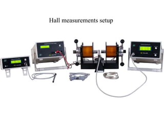
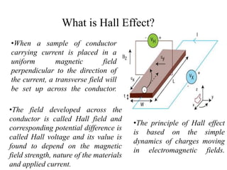
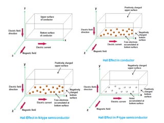
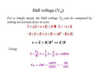
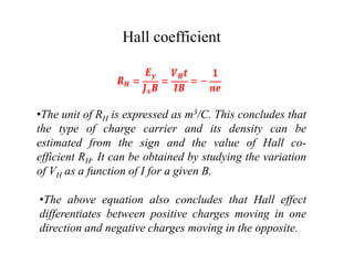
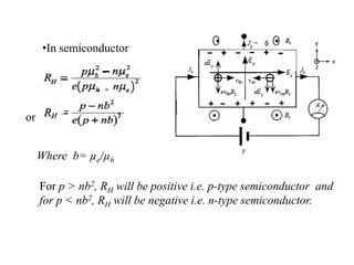
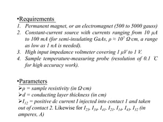
The document discusses the Hall effect, which is when a conductor carrying an electric current is placed perpendicular to a magnetic field. This causes the charges in the conductor to experience a force perpendicular to both the current and the magnetic field. This displacement of charges establishes a voltage difference known as the Hall voltage across the conductor. The Hall effect can be used to determine various properties of materials like charge carrier types and densities. Precise measurement techniques like Van der Pauw and Hall coefficient calculations are used to characterize semiconductor samples.


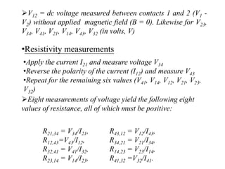
![2.The sample type is determined from the polarity of the
voltage sum VC + VD + VE + VF. If this sum is positive
(negative), the sample is p-type (n-type).
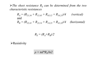
3.The sheet carrier density (in units of cm-2) is calculated
from
ps = 8*10-8IB/[q(VC + VD + VE + VF)]
if the voltage sum is positive, or
ns = |8*10-8 IB/[q(VC + VD + VE + VF)]|
if the voltage sum is negative,
where B is the magnetic field in gauss (G) and I is the dc
current in amperes (A).
4.The bulk carrier density (in units of cm-3) can be
determined as follows if the conducting layer thickness d
of the sample is known:
n = ns/d p = ps/d](https://image.slidesharecdn.com/halleffect-180809054215/85/Hall-effect-13-320.jpg)
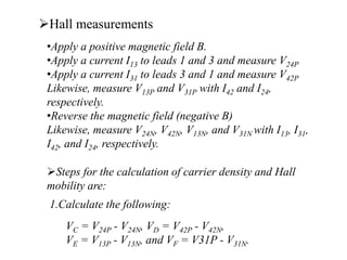
![5.The Hall mobility μ = 1/qnsRS (in units of cm2V-1s-1) is
calculated from the sheet carrier density ns (or ps) and the
sheet resistance RS.
Hall coefficient
Eight resistances on the application of magnetic field are
R24,13 = V24P/I13, R42,31 = V42P/I31, for (+)B
R13,42 = V13P/I42, R31,42 =V31P/I42.
R24,13 = V24N/I13, R42,31 = V42N/I31, for (-)B
R13,42 = V13N/I42, R31,42 =V31N/I42.
RH = d/8B*[R24,13(+B)-R24,13(-B)+R42,31(+B)-
R42,31(-B)+R13,42-(+B)- R13,42(-B)+R31,42(+B)-R31,42(-B)]](https://image.slidesharecdn.com/halleffect-180809054215/85/Hall-effect-14-320.jpg)