
Recommended
Recommended
More Related Content
What's hot
What's hot (20)
Similar to Original Power MOSFET IRFP140PBF IRFP140 IRFP140N 100V 33A TO-247 New International Rectifier
Similar to Original Power MOSFET IRFP140PBF IRFP140 IRFP140N 100V 33A TO-247 New International Rectifier (14)
More from AUTHELECTRONIC
More from AUTHELECTRONIC (20)
Recently uploaded
Recently uploaded (20)
Original Power MOSFET IRFP140PBF IRFP140 IRFP140N 100V 33A TO-247 New International Rectifier
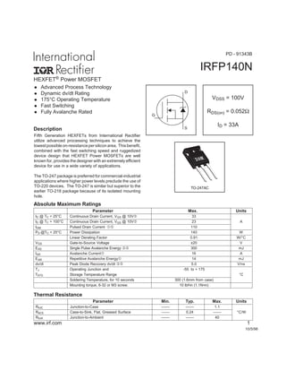
- 1. HEXFET® Power MOSFET IRFP140N Fifth Generation HEXFETs from International Rectifier utilize advanced processing techniques to achieve the lowestpossibleon-resistancepersiliconarea. Thisbenefit, combined with the fast switching speed and ruggedized device design that HEXFET Power MOSFETs are well known for, provides the designer with an extremely efficient device for use in a wide variety of applications. The TO-247 package is preferred for commercial-industrial applications where higher power levels preclude the use of TO-220 devices. The TO-247 is similar but superior to the earlier TO-218 package because of its isolated mounting hole. l Advanced Process Technology l Dynamic dv/dt Rating l 175°C Operating Temperature l Fast Switching l Fully Avalanche Rated Description 10/5/98 VDSS = 100V RDS(on) = 0.052Ω ID = 33AS D G Parameter Min. Typ. Max. Units RθJC Junction-to-Case –––– –––– 1.1 RθCS Case-to-Sink, Flat, Greased Surface –––– 0.24 –––– °C/W RθJA Junction-to-Ambient –––– –––– 40 Thermal Resistance Parameter Max. Units ID @ TC = 25°C Continuous Drain Current, VGS @ 10V… 33 ID @ TC = 100°C Continuous Drain Current, VGS @ 10V… 23 A IDM Pulsed Drain Current … 110 PD @TC = 25°C Power Dissipation 140 W Linear Derating Factor 0.91 W/°C VGS Gate-to-Source Voltage ±20 V EAS Single Pulse Avalanche Energy ‚… 300 mJ IAR Avalanche Current 16 A EAR Repetitive Avalanche Energy 14 mJ dv/dt Peak Diode Recovery dv/dt ƒ… 5.0 V/ns TJ Operating Junction and -55 to + 175 TSTG Storage Temperature Range °C Soldering Temperature, for 10 seconds 300 (1.6mm from case) Mounting torque, 6-32 or M3 screw. 10 lbf•in (1.1N•m) Absolute Maximum Ratings TO-247AC www.irf.com 1 PD - 91343B
- 2. IRFP140N 2 www.irf.com Parameter Min. Typ. Max. Units Conditions V(BR)DSS Drain-to-Source Breakdown Voltage 100 ––– ––– V VGS = 0V, ID = 250µA ∆V(BR)DSS/∆TJ Breakdown Voltage Temp. Coefficient ––– 0.11 ––– V/°C Reference to 25°C, ID = 1mA… RDS(on) Static Drain-to-Source On-Resistance ––– ––– 0.052 Ω VGS = 10V, ID = 16A „ VGS(th) Gate Threshold Voltage 2.0 ––– 4.0 V VDS = VGS, ID = 250µA gfs Forward Transconductance 11 ––– ––– S VDS = 50V, ID = 16A… ––– ––– 25 VDS = 100V, VGS = 0V ––– ––– 250 VDS = 80V, VGS = 0V, TJ = 150°C Gate-to-Source Forward Leakage ––– ––– 100 VGS = 20V Gate-to-Source Reverse Leakage ––– ––– -100 VGS = -20V Qg Total Gate Charge ––– ––– 94 ID = 16A Qgs Gate-to-Source Charge ––– ––– 15 nC VDS = 80V Qgd Gate-to-Drain ("Miller") Charge ––– ––– 43 VGS = 10V, See Fig. 6 and 13 „… td(on) Turn-On Delay Time ––– 8.2 ––– VDD = 50V tr Rise Time ––– 39 ––– ID = 16A td(off) Turn-Off Delay Time ––– 44 ––– RG = 5.1Ω tf Fall Time ––– 33 ––– RD = 3.0Ω, See Fig. 10 „… Between lead, 6mm (0.25in.) from package and center of die contact Ciss Input Capacitance ––– 1400 ––– VGS = 0V Coss Output Capacitance ––– 330 ––– pF VDS = 25V Crss Reverse Transfer Capacitance ––– 170 ––– ƒ = 1.0MHz, See Fig. 5… nH µA nA IDSS Drain-to-Source Leakage Current IGSS LS Internal Source Inductance ––– ––– ns S D G 5.0 13 Electrical Characteristics @ TJ = 25°C (unless otherwise specified) ––– LD Internal Drain Inductance –––––– ––– Notes: Repetitive rating; pulse width limited by max. junction temperature. ( See fig. 11 ) ƒ ISD ≤ 16A, di/dt ≤ 210A/µs, VDD ≤ V(BR)DSS, TJ ≤ 175°C „ Pulse width ≤ 300µs; duty cycle ≤ 2%.‚ VDD = 25V, starting TJ = 25°C, L = 2.0mH RG = 25Ω, IAS = 16A. (See Figure 12) Parameter Min. Typ. Max. Units Conditions IS Continuous Source Current MOSFET symbol (Body Diode) showing the ISM Pulsed Source Current integral reverse (Body Diode) … p-n junction diode. VSD Diode Forward Voltage ––– ––– 1.3 V TJ = 25°C, IS = 16A, VGS = 0V „ trr Reverse Recovery Time ––– 170 250 ns TJ = 25°C, IF = 16A Qrr Reverse RecoveryCharge ––– 1.1 1.6 µC di/dt = 100A/µs „… Source-Drain Ratings and Characteristics A ––– ––– 110 ––– ––– 33 S D G … Uses IRF540N data and test conditions.
- 3. IRFP140N www.irf.com 3 Fig 1. Typical Output Characteristics Fig 3. Typical Transfer Characteristics Fig 4. Normalized On-Resistance Vs. Temperature Fig 2. Typical Output Characteristics 1 10 100 1000 0.1 1 10 100 I,Drain-to-SourceCurrent(A) D V , Drain-to-Source Voltage (V)DS VGS TOP 15V 10V 8.0V 7.0V 6.0V 5.5V 5.0V BOTTOM 4.5V 20µs PULSE W IDTH T = 25°CC A 4.5V 1 10 100 1000 0.1 1 10 100 4.5V I,Drain-to-SourceCurrent(A) D V , Drain-to-Source Voltage (V)DS VGS TOP 15V 10V 8.0V 7.0V 6.0V 5.5V 5.0V BOTTOM 4.5V 20µs PULSE W IDTH T = 175°CC A 1 10 100 1000 4 5 6 7 8 9 10 T = 25°CJ GSV , Gate-to-Source Voltage (V) DI,Drain-to-SourceCurrent(A) V = 50V 20µs PULSE W IDTH DS T = 175°CJ A 0.0 0.5 1.0 1.5 2.0 2.5 3.0 -60 -40 -20 0 20 40 60 80 100 120 140 160 180 JT , Junction Temperature (°C) R,Drain-to-SourceOnResistanceDS(on) (Normalized) V = 10VGS A I = 27AD
- 4. IRFP140N 4 www.irf.com Fig 7. Typical Source-Drain Diode Forward Voltage Fig 5. Typical Capacitance Vs. Drain-to-Source Voltage Fig 8. Maximum Safe Operating Area Fig 6. Typical Gate Charge Vs. Gate-to-Source Voltage 0 400 800 1200 1600 2000 2400 1 10 100 C,Capacitance(pF) DSV , Drain-to-Source Voltage (V) A V = 0V , f = 1MHz C = C + C , C SHORTE D C = C C = C + C GS iss gs gd ds rss gd oss ds gdCiss Coss Crss 0 4 8 12 16 20 0 20 40 60 80 100 Q , Total Gate Charge (nC)GV,Gate-to-SourceVoltage(V)GS V = 80V V = 50V V = 20V DS DS DS A FOR TEST CIRCUIT SEE FIGURE 13 I = 16AD 10 100 1000 0.4 0.8 1.2 1.6 2.0 T = 25°CJ V = 0VGS V , Source-to-Drain Voltage (V) I,ReverseDrainCurrent(A) SD SD A T = 175°CJ 1 10 100 1000 1 10 100 1000 V , Drain-to-Source Voltage (V)DS I,DrainCurrent(A) OPE RATION IN THIS AREA LIMITE D BY R D DS(on) 10µs 100µs 1ms 10ms A T = 25°C T = 175°C S ingle Pulse C J
- 5. IRFP140N www.irf.com 5 Fig 9. Maximum Drain Current Vs. Case Temperature Fig 10a. Switching Time Test Circuit VDS 90% 10% VGS td(on) tr td(off) tf VDS Pulse Width ≤ 1 µs Duty Factor ≤ 0.1 % Fig 10b. Switching Time Waveforms RD VGS RG D.U.T. 10V Fig 11. Maximum Effective Transient Thermal Impedance, Junction-to-Case + -VDD 25 50 75 100 125 150 175 0 5 10 15 20 25 30 35 T , Case Temperature ( C) I,DrainCurrent(A) °C D 0.01 0.1 1 10 0.00001 0.0001 0.001 0.01 0.1 1 Notes: 1. Duty factor D = t / t 2. Peak T = P x Z + T 1 2 J DM thJC C P t t DM 1 2 t , Rectangular Pulse Duration (sec) ThermalResponse(Z) 1 thJC 0.01 0.02 0.05 0.10 0.20 D = 0.50 SINGLE PULSE (THERMAL RESPONSE)
- 6. IRFP140N 6 www.irf.com Fig 12a. Unclamped Inductive Test Circuit VDS L D.U.T. VDD IAS tp 0.01Ω RG + - tp VDS IAS VDD V(BR)DSS 10 V Fig 12b. Unclamped Inductive Waveforms D.U.T. VDS IDIG 3mA VGS .3µF 50KΩ .2µF12V Current Regulator Same Type as D.U.T. Current Sampling Resistors + - Fig 13b. Gate Charge Test Circuit QG QGS QGD VG Charge 10 V Fig 13a. Basic Gate Charge Waveform Fig 12c. Maximum Avalanche Energy Vs. Drain Current 0 100 200 300 400 500 600 700 25 50 75 100 125 150 175 J E,SinglePulseAvalancheEnergy(mJ)AS A Starting T , Junction Temperature (°C) V = 25V I TOP 6.6A 11A BOTTOM 16A DD D
- 7. IRFP140N www.irf.com 7 P.W. Period di/dt Diode Recovery dv/dt Ripple ≤ 5% Body Diode Forward Drop Re-Applied Voltage Reverse Recovery Current Body Diode Forward Current VGS=10V VDD ISD Driver Gate Drive D.U.T. ISD Waveform D.U.T. VDS Waveform Inductor Curent D = P.W. Period + - + + +- - - Fig 14. For N-Channel HEXFETS * VGS = 5V for Logic Level Devices Peak Diode Recovery dv/dt Test Circuit ƒ „ ‚ RG VDD • dv/dt controlled by RG • Driver same type as D.U.T. • ISD controlled by Duty Factor "D" • D.U.T. - Device Under Test D.U.T Circuit Layout Considerations • Low Stray Inductance • Ground Plane • Low Leakage Inductance Current Transformer *
- 8. IRFP140N 8 www.irf.com Package Outline TO-247AC Outline Dimensions are shown in millimeters (inches) TO-247AC Part Marking Information LEAD ASSIGNMENTS NOTES: - D - 5.30 (.209) 4.70 (.185) 2.50 (.089) 1.50 (.059) 4 3X 0.80 (.031) 0.40 (.016) 2.60 (.102) 2.20 (.087)3.40 (.133) 3.00 (.118) 3X 0.25 (.010) M C A S 4.30 (.170) 3.70 (.145) - C - 2X 5.50 (.217) 4.50 (.177) 5.50 (.217) 0.25 (.010) 1.40 (.056) 1.00 (.039) 3.65 (.143) 3.55 (.140) DM MB - A - 15.90 (.626) 15.30 (.602) - B - 1 2 3 20.30 (.800) 19.70 (.775) 14.80 (.583) 14.20 (.559) 2.40 (.094) 2.00 (.079) 2X 2X 5.45 (.215) 1 DIMENSIONING & TOLERANCING PER ANSI Y14.5M, 1982. 2 CONTROLLING DIMENSION : INCH. 3 CONFORMS TO JEDEC OUTLINE TO-247-AC. 1 - GATE 2 - DRAIN 3 - SOURCE 4 - DRAIN IN TERN ATIO NAL RECTIFIER LOG O ASSEM BLY LOT COD E EXAM PLE : TH IS IS AN IR FPE30 W ITH ASSEM BLY LOT CO DE 3A1Q PAR T NU MBER D ATE C ODE (YYW W ) YY = YEAR W W W EEK 3A1Q 9302 IR FPE30 A WORLD HEADQUARTERS: 233 Kansas St., El Segundo, California 90245, Tel: (310) 322 3331 IR GREAT BRITAIN: Hurst Green, Oxted, Surrey RH8 9BB, UK Tel: ++ 44 1883 732020 IR CANADA: 15 Lincoln Court, Brampton, Ontario L6T3Z2, Tel: (905) 453 2200 IR GERMANY: Saalburgstrasse 157, 61350 Bad Homburg Tel: ++ 49 6172 96590 IR ITALY: Via Liguria 49, 10071 Borgaro, Torino Tel: ++ 39 11 451 0111 IR FAR EAST: K&H Bldg., 2F, 30-4 Nishi-Ikebukuro 3-Chome, Toshima-Ku, Tokyo Japan 171 Tel: 81 3 3983 0086 IR SOUTHEAST ASIA: 1 Kim Seng Promenade, Great World City West Tower, 13-11, Singapore 237994 Tel: ++ 65 838 4630 IR TAIWAN:16 Fl. Suite D. 207, Sec. 2, Tun Haw South Road, Taipei, 10673, Taiwan Tel: 886-2-2377-9936 http://www.irf.com/ Data and specifications subject to change without notice. 8/98