
Recommended
Recommended
More Related Content
What's hot
What's hot (20)
Similar to Original IGBT IRG4BC20KD-S G4BC20KD 600V 9A TO-263 New
Similar to Original IGBT IRG4BC20KD-S G4BC20KD 600V 9A TO-263 New (14)
More from AUTHELECTRONIC
More from AUTHELECTRONIC (20)
Recently uploaded
Recently uploaded (20)
Original IGBT IRG4BC20KD-S G4BC20KD 600V 9A TO-263 New
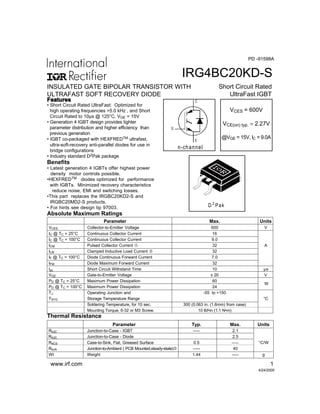
- 1. Parameter Max. Units VCES Collector-to-Emitter Voltage 600 V IC @ TC = 25°C Continuous Collector Current 16 IC @ TC = 100°C Continuous Collector Current 9.0 ICM Pulsed Collector Current Q 32 A ILM Clamped Inductive Load Current R 32 IF @ TC = 100°C Diode Continuous Forward Current 7.0 IFM Diode Maximum Forward Current 32 tsc Short Circuit Withstand Time 10 µs VGE Gate-to-Emitter Voltage ± 20 V PD @ TC = 25°C Maximum Power Dissipation 60 PD @ TC = 100°C Maximum Power Dissipation 24 TJ Operating Junction and -55 to +150 TSTG Storage Temperature Range °C Soldering Temperature, for 10 sec. 300 (0.063 in. (1.6mm) from case) Mounting Torque, 6-32 or M3 Screw. 10 lbf•in (1.1 N•m) IRG4BC20KD-S INSULATED GATE BIPOLAR TRANSISTOR WITH ULTRAFAST SOFT RECOVERY DIODE FeaturesFeaturesFeaturesFeaturesFeatures E G n-channel C VCES = 600V VCE(on) typ. = 2.27V @VGE = 15V, IC = 9.0A Short Circuit Rated UltraFast IGBT 4/24/2000 • Short Circuit Rated UltraFast: Optimized for high operating frequencies >5.0 kHz , and Short Circuit Rated to 10µs @ 125°C, VGE = 15V • Generation 4 IGBT design provides tighter parameter distribution and higher efficiency than previous generation • IGBT co-packaged with HEXFREDTM ultrafast, ultra-soft-recovery anti-parallel diodes for use in bridge configurations • Industry standard D2Pak package Benefits • Latest generation 4 IGBTs offer highest power density motor controls possible. •HEXFREDTM diodes optimized for performance with IGBTs. Minimized recovery characteristics reduce noise, EMI and switching losses. •This part replaces the IRGBC20KD2-S and IRGBC20MD2-S products. • For hints see design tip 97003. PD -91598A Absolute Maximum Ratings W 2 D Pak Parameter Typ. Max. Units RθJC Junction-to-Case - IGBT ––– 2.1 RθJC Junction-to-Case - Diode 2.5 RθCS Case-to-Sink, Flat, Greased Surface 0.5 ––– °C/W RθJA Junction-to-Ambient ( PCB Mounted,steady-state)U ––– 40 Wt Weight 1.44 ––– g Thermal Resistance www.irf.com 1
- 2. IRG4BC20KD-S 2 www.irf.com Parameter Min. Typ. Max. Units Conditions Qg Total Gate Charge (turn-on) — 34 51 IC = 9.0A Qge Gate - Emitter Charge (turn-on) — 4.9 7.4 nC VCC = 400V See Fig.8 Qgc Gate - Collector Charge (turn-on) — 14 21 VGE = 15V td(on) Turn-On Delay Time — 54 — tr Rise Time — 34 — TJ = 25°C td(off) Turn-Off Delay Time — 180 270 IC = 9.0A, VCC = 480V tf Fall Time — 72 110 VGE = 15V, RG = 50Ω Eon Turn-On Switching Loss — 0.34 — Energy losses include "tail" Eoff Turn-Off Switching Loss — 0.30 — mJ and diode reverse recovery Ets Total Switching Loss — 0.64 0.96 See Fig. 9,10,14 tsc Short Circuit Withstand Time 10 — — µs VCC = 360V, TJ = 125°C VGE = 15V, RG = 50Ω , VCPK < 500V td(on) Turn-On Delay Time — 51 — TJ = 150°C, See Fig. 11,14 tr Rise Time — 37 — IC = 9.0A, VCC = 480V td(off) Turn-Off Delay Time — 220 — VGE = 15V, RG = 50Ω tf Fall Time — 160 — Energy losses include "tail" Ets Total Switching Loss — 0.85 — mJ and diode reverse recovery LE Internal Emitter Inductance — 7.5 — nH Measured 5mm from package Cies Input Capacitance — 450 — VGE = 0V Coes Output Capacitance — 61 — pF VCC = 30V See Fig. 7 Cres Reverse Transfer Capacitance — 14 — ƒ = 1.0MHz trr Diode Reverse Recovery Time — 37 55 ns TJ = 25°C See Fig. — 55 90 TJ = 125°C 14 IF = 8.0A Irr Diode Peak Reverse Recovery Current — 3.5 5.0 A TJ = 25°C See Fig. — 4.5 8.0 TJ = 125°C 15 VR = 200V Qrr Diode Reverse Recovery Charge — 65 138 nC TJ = 25°C See Fig. — 124 360 TJ = 125°C 16 di/dt = 200Aµs di(rec)M/dt Diode Peak Rate of Fall of Recovery — 240 — A/µs TJ = 25°C See Fig. During tb — 210 — TJ = 125°C 17 Parameter Min. Typ. Max. Units Conditions V(BR)CES Collector-to-Emitter Breakdown VoltageS 600 — — V VGE = 0V, IC = 250µA ∆V(BR)CES/∆TJ Temperature Coeff. of Breakdown Voltage — 0.49 — V/°C VGE = 0V, IC = 1.0mA VCE(on) Collector-to-Emitter Saturation Voltage — 2.27 2.8 IC = 9.0A VGE = 15V — 3.01 — V IC = 16A See Fig. 2, 5 — 2.43 — IC = 9.0A, TJ = 150°C VGE(th) Gate Threshold Voltage 3.0 — 6.0 VCE = VGE, IC = 250µA ∆VGE(th)/∆TJ Temperature Coeff. of Threshold Voltage — -10 — mV/°C VCE = VGE, IC = 250µA gfe Forward Transconductance T 2.9 4.3 — S VCE = 100V, IC = 9.0A ICES Zero Gate Voltage Collector Current — — 250 µA VGE = 0V, VCE = 600V — — 1000 VGE = 0V, VCE = 600V, TJ = 150°C VFM Diode Forward Voltage Drop — 1.4 1.7 V IC = 8.0A See Fig. 13 — 1.3 1.6 IC = 8.0A, TJ = 150°C IGES Gate-to-Emitter Leakage Current — — ±100 nA VGE = ±20V Switching Characteristics @ TJ = 25°C (unless otherwise specified) Electrical Characteristics @ TJ = 25°C (unless otherwise specified) ns ns
- 3. IRG4BC20KD-S www.irf.com 3 0.1 1 10 100 0.0 0.5 1.0 1.5 2.0 2.5 f, Frequency (KHz) LOADCURRENT(A) Fig. 1 - Typical Load Current vs. Frequency (Load Current = IRMS of fundamental) For both: Duty cycle: 50% T = 125°C T = 90°C Gate drive as specified sink J Power Dissipation = W 60% of rated voltage I Ideal diodes Square wave: 1.8 Fig. 2 - Typical Output Characteristics Fig. 3 - Typical Transfer Characteristics 1 10 100 1 10 V , Collector-to-Emitter Voltage (V) I,Collector-to-EmitterCurrent(A) CE C V = 15V 20µs PULSE WIDTH GE T = 25 CJ o T = 150 CJ o 1 10 100 5 10 15 20 V , Gate-to-Emitter Voltage (V) I,Collector-to-EmitterCurrent(A) GE C V = 50V 5µs PULSE WIDTH CC T = 25 CJ o T = 150 CJ o 55°C
- 4. IRG4BC20KD-S 4 www.irf.com Fig. 6 - Maximum Effective Transient Thermal Impedance, Junction-to-Case Fig. 5 - Typical Collector-to-Emitter Voltage vs. Junction Temperature Fig. 4 - Maximum Collector Current vs. Case Temperature -60 -40 -20 0 20 40 60 80 100 120 140 160 1.0 2.0 3.0 4.0 5.0 T , Junction Temperature ( C) V,Collector-to-EmitterVoltage(V) J ° CE V = 15V 80 us PULSE WIDTH GE I = A4.5C I = A9C I = A18C 25 50 75 100 125 150 0 5 10 15 20 T , Case Temperature ( C) MaximumDCCollectorCurrent(A) C ° 0.01 0.1 1 10 0.00001 0.0001 0.001 0.01 0.1 1 Notes: 1. Duty factor D = t / t 2. Peak T = P x Z + T 1 2 J DM thJC C P t t DM 1 2 t , Rectangular Pulse Duration (sec) ThermalResponse(Z) 1 thJC 0.01 0.02 0.05 0.10 0.20 D = 0.50 SINGLE PULSE (THERMAL RESPONSE) 9.0A
- 5. IRG4BC20KD-S www.irf.com 5 0 10 20 30 40 50 0.5 0.6 0.7 0.8 R , Gate Resistance (Ohm) TotalSwitchingLosses(mJ) G V = 480V V = 15V T = 25 C I = 9.0A CC GE J C ° Fig. 7 - Typical Capacitance vs. Collector-to-Emitter Voltage Fig. 8 - Typical Gate Charge vs. Gate-to-Emitter Voltage Fig. 9 - Typical Switching Losses vs. Gate Resistance Fig. 10 - Typical Switching Losses vs. Junction Temperature 0 10 20 30 40 0 4 8 12 16 20 Q , Total Gate Charge (nC) V,Gate-to-EmitterVoltage(V) G GE V = 400V I = 9.0A CC C 1 10 100 0 200 400 600 800 V , Collector-to-Emitter Voltage (V) C,Capacitance(pF) CE V C C C = = = = 0V, C C C f = 1MHz + C + C C SHORTED GE ies ge gc , ce res gc oes ce gc Cies Coes Cres RG , Gate Resistance ( Ω ) -60 -40 -20 0 20 40 60 80 100 120 140 160 0.1 1 10 T , Junction Temperature ( C ) TotalSwitchingLosses(mJ) J ° R = Ohm V = 15V V = 480V G GE CC I = A18C I = A9C I = A4.5C 50Ω 9.0A
- 6. IRG4BC20KD-S 6 www.irf.com Fig. 11 - Typical Switching Losses vs. Collector-to-Emitter Current Fig. 12 - Turn-Off SOA 1 10 100 1 10 100 1000 V = 20V T = 125 C GE J o V , Collector-to-Emitter Voltage (V)I,Collector-to-EmitterCurrent(A) CEC SAFE OPERATING AREA Fig. 13 - Maximum Forward Voltage Drop vs. Instantaneous Forward Current 0.1 1 10 100 0.4 0.8 1.2 1.6 2.0 2.4 2.8 3.2 FM FInstantaneousForwardCurrent-I(A) Forward Voltage Drop - V (V) T = 150°C T = 125°C T = 25°C J J J 0 4 8 12 16 20 0.0 1.0 2.0 3.0 I , Collector-to-emitter Current (A) TotalSwitchingLosses(mJ) C R = Ohm T = 150 C V = 480V V = 15V G J CC GE ° 50Ω
- 7. IRG4BC20KD-S www.irf.com 7 Fig. 14 - Typical Reverse Recovery vs. dif/dt Fig. 15 - Typical Recovery Current vs. dif/dt Fig. 16 - Typical Stored Charge vs. dif/dt Fig. 17 - Typical di(rec)M/dt vs. dif/dt 0 100 200 300 400 500 100 1000 fdi /dt - (A/µs) RRQ-(nC) I = 16A I = 8.0A I = 4.0AF F F V = 200V T = 125°C T = 25°C R J J 100 1000 10000 100 1000 fdi /dt - (A/µs) di(rec)M/dt-(A/µs) I = 16A I = 8.0A I = 4.0A F F F V = 200V T = 125°C T = 25°C R J J 0 20 40 60 80 100 100 1000 fdi /dt - (A/µs) t-(ns)rr I = 16A I = 8.0A I = 4.0A F F F V = 200V T = 125°C T = 25°C R J J 1 10 100 100 1000 fdi /dt - (A/µs) I-(A)IRRM I = 16A I = 8.0A I = 4.0AF F F V = 200V T = 125°C T = 25°C R J J
- 8. IRG4BC20KD-S 8 www.irf.com Same type device as D.U.T. D.U.T. 430µF 80% of Vce Fig. 18a - Test Circuit for Measurement of ILM, Eon, Eoff(diode), trr, Qrr, Irr, td(on), tr, td(off), tf t1 Ic Vce t1 t2 90% Ic 10% Vce td(off) tf Ic 5% Ic t1+5µS Vce ic dt 90% Vge +Vge ∫Eoff = Fig. 18b - Test Waveforms for Circuit of Fig. 18a, Defining Eoff, td(off), tf ∫Vce ie dt t2 t1 5% Vce Ic IpkVcc 10% Ic Vce t1 t2 D UT VO LTAGE AN D CU RRE NT GATE VOLTA GE D .U .T. +Vg 10% +Vg 90% Ic trtd(on) DIO DE REVE RSE REC OVERY ENER GY tx E on = ∫Erec = t4 t3 Vd id dt t4t3 DIODE RE COV ERY W AVEFO RMS Ic V pk 10% Vcc Irr 10% Irr Vcc trr ∫Q rr = trr tx id dt Fig. 18c - Test Waveforms for Circuit of Fig. 18a, Defining Eon, td(on), tr Fig. 18d - Test Waveforms for Circuit of Fig. 18a, Defining Erec, trr, Qrr, Irr Vd Ic dt Vce Ic dt Ic dt Vce Ic dt
- 9. IRG4BC20KD-S www.irf.com 9 Vg GATE SIGNAL DEVICE UNDER TEST CURRENT D.U.T. VOLTAGE IN D.U.T. CURRENT IN D1 t0 t1 t2 D.U.T. V *c 5 0 V L 1000V 6000µF 100V Figure 19. Clamped Inductive Load Test Circuit Figure 20. Pulsed Collector Current Test Circuit RL= 480V 4 X IC @25°C 0 - 480V Figure 18e. Macro Waveforms for Figure 18a's Test Circuit Tape Reel Information D2Pak 3 4 4 TR R FEED D IRECTION 1.85 (.0 73) 1.65 (.0 65) 1.60 (.063) 1.50 (.059) 4.10 (.161) 3.90 (.153) TRL FE ED DIRE CTION 10.90 (.429) 10.70 (.421) 16.10 (.634) 15.90 (.626) 1.75 (.069) 1.25 (.049) 11.60 (.457) 11.40 (.449) 15.42 (.609) 15.22 (.601) 4.72 (.136) 4.52 (.178) 24.30 (.957) 23.90 (.941) 0.368 (.0145) 0.342 (.0135) 1.60 (.063) 1.50 (.059) 13.50 (.532) 12.80 (.504) 330.00 (14.173) MAX. 27.40 (1.079) 23.90 (.941) 60.00 (2.362) MIN. 30.40 (1.197) MAX. 26.40 (1.039) 24.40 (.961) NOTES : 1. CO MFORMS TO EIA-418. 2. CO NTRO LLING DIMENSIO N: MILLIMETER. 3. DIMENSIO N MEASUR ED @ HU B. 4. INCLUDES FLANG E DISTORTIO N @ OUTER EDGE.
- 10. IRG4BC20KD-S 10 www.irf.com 1 0.16 (.40 0) REF . 6.47 (.25 5) 6.18 (.24 3) 2.61 (.10 3) 2.32 (.09 1) 8.8 9 (.35 0) R E F. - B - 1.32 (.0 52) 1.22 (.0 48) 2.79 (.1 10) 2.29 (.0 90) 1 .39 (.055 ) 1 .14 (.045 ) 5 .28 (.2 08 ) 4 .78 (.1 88 ) 4.69 (.18 5) 4.20 (.16 5) 10.5 4 (.4 15) 10.2 9 (.4 05) - A - 2 1 3 1 5.49 (.61 0) 1 4.73 (.58 0) 3 X 0.9 3 (.0 37) 0.6 9 (.0 27) 5.08 (.20 0) 3 X 1.40 (.0 55) 1.14 (.0 45) 1.78 (.07 0) 1.27 (.05 0) 1.40 (.055 ) M A X. N O T ES : 1 D IM EN S IO N S AF T E R S OL D ER D IP. 2 D IM EN S IO N ING TO L ERA N C IN G P ER AN SI Y 14 .5M , 198 2. 3 C O NT RO L LIN G D IM E NSIO N : IN C H. 4 H EAT SINK LE AD D IM EN S IO N S DO N O T INC L UD E BUR R S. 0.55 (.0 22) 0.46 (.0 18) 0.25 (.0 10) M B A M M IN IM U M R E CO M M EN DE D F O OT PR IN T 11 .43 (.4 50 ) 8.89 (.3 50 ) 17.7 8 (.7 00 ) 3 .8 1 (.150 ) 2 .08 (.082 ) 2X LEA D A SS IG NM EN T S 1 - G A TE 2 - D R AIN 3 - S O U RC E 2.5 4 (.1 00) 2X D2Pak Package Outline Notes: QRepetitiverating:VGE=20V;pulsewidthlimitedbymaximumjunctiontemperature(figure20) RVCC=80%(VCES),VGE=20V,L=10µH,RG=50Ω(figure19) SPulsewidth≤80µs;dutyfactor≤0.1%. TPulsewidth5.0µs,singleshot. U When mounted on 1 square PCB (FR-4 or G-10 Material ). For recommended footprint and soldering techniques refer to application note #AN-994. IR WORLD HEADQUARTERS: 233 Kansas St., El Segundo, California 90245, USA Tel: (310) 252-7105 IR EUROPEAN REGIONAL CENTRE: 439/445 Godstone Rd, Whyteleafe, Surrey CR3 OBL, UK Tel: ++ 44 (0)20 8645 8000 IR CANADA: 15 Lincoln Court, Brampton, Ontario L6T3Z2, Tel: (905) 453 2200 IR GERMANY: Saalburgstrasse 157, 61350 Bad Homburg Tel: ++ 49 (0) 6172 96590 IR ITALY: Via Liguria 49, 10071 Borgaro, Torino Tel: ++ 39 011 451 0111 IR JAPAN: KH Bldg., 2F, 30-4 Nishi-Ikebukuro 3-Chome, Toshima-Ku, Tokyo 171 Tel: 81 (0)3 3983 0086 IR SOUTHEAST ASIA: 1 Kim Seng Promenade, Great World City West Tower, 13-11, Singapore 237994 Tel: ++ 65 (0)838 4630 IR TAIWAN:16 Fl. Suite D. 207, Sec. 2, Tun Haw South Road, Taipei, 10673 Tel: 886-(0)2 2377 9936 Data and specifications subject to change without notice. 10/00
- 11. Note: For the most current drawings please refer to the IR website at: http://www.irf.com/package/