Introducing the IXRFDSM607X2 Dual RF Driver

Visit the IXRFDSM607X2 Web Page: https://ixysrf.com/product/ixrfdsm607x2/ The IXRFDSM607X2 is a dual CMOS high-speed, high-current gate driver specifically designed to drive MOSFETs in Class D and E HF RF applications as well as other applications requiring ultrafast rise and fall times or short minimum pulse widths. The IXRFDSM607X2 can source and sink 7 A of peak current per driver, 15 A when combined, while producing voltage rise and fall times of less than 5 ns and minimum pulse widths of 8 ns. The inputs of the driver are compatible with TTL or CMOS and are fully immune to latch up over the entire operating range. Designed with small internal delays, cross conduction or current shoot-through is virtually eliminated. The features and wide safety margin in operating voltage and power make the IXRFDSM607X2 unmatched in performance and value. The surface mount IXRFDSM607X2 is packaged in a low-inductance surface mount package incorporating advanced layout techniques to minimize stray lead inductances for optimum switching performance. The input and output pins can be separated or combined for dual or single driver operation. However, both sides are ground referenced together and cannot be operated ground isolated from each other.. Features High Peak Output Current Low Output Impedance Low Quiescent Supply Current Low Propagation Delay High Capacitive Load Drive Capability Wide Operating Voltage Range Single or Dual Driver Operation Capable Advantages Optimized for RF and high speed Easy to mount, no insulators needed High power density RoHS compliant Applications RF MOSFET Driver Class D and E RF Generators Multi-MHz Switch Mode Power Supplies Pulse Transformer Drivers Pulse Laser Diode Drivers Pulse Generators

Recommended
Recommended
More Related Content
What's hot
What's hot (20)
Similar to Introducing the IXRFDSM607X2 Dual RF Driver
Similar to Introducing the IXRFDSM607X2 Dual RF Driver (20)
More from Directed Energy, Inc.
Recently uploaded
Recently uploaded (20)
Introducing the IXRFDSM607X2 Dual RF Driver
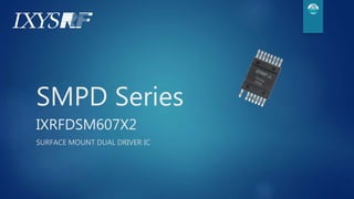
- 1. SMPD Series IXRFDSM607X2 SURFACE MOUNT DUAL DRIVER IC
- 2. Sales Webinar Welcome Introductions Steve Krausse Gib Bates Recorded Webinar Can you hear the Audio? Can you see the video & presentation? Chat Function Questions Public Private sales@ixysrf.com +1-970-493-1901 Webinar Feedback How can we improve? Rate the webinar! 2
- 3. What We’ll Cover Markets Pricing/Availability Technical Overview Features Advantages Device Details Configuration Details Driver and SPICE Model Construction Demonstration Board Solutions for Common Issues Applications Q&A 3
- 4. Markets 4 RF power generation Pulse-to-Pulse high speed switching for diode applications Thin film deposition Induction heating Power conversion
- 5. Pricing & Availability US MSRP $27.66 Rail Quantity: 30 ea. Outside the US Taxes Tariffs Import Duties Shipping/Delivery Costs Etc. 5 Availability Current: Mid-October 2017 Normal: Stock to 8-10 Weeks Digikey
- 6. Technical Overview Speaker: Gib Bates, IXYSRF R&D 6
- 7. What’s New? DE packaging SMPD packaging 7 DE package has wide flat silver plated lead-frame Typically needs lead forming for strain relief caused by thermal cycling MSL 3 1 week limited exposure time Beveled drain lead and case for orientation Surface Mount Power Device has tin plated gull wing lead-frame No special lead forming required MSL 1 unlimited exposure time Missing pin for orientation Utilizes same die line-up as our DE packaging
- 8. Features Dual 7.5A or 15A combined peak sink / source current Wide operating voltage range Low output impedance High capacitive load drive capability Less than 10ns rise and fall times Low minimum pulse width High power density 8
- 9. Advantages 9 Optimized for RF and high speed switching Gull wing lead-frame incorporates thermal strain relief No lead forming required Automated assembly capable Isolated substrate, no insulating pads required RoHS compliant
- 10. Technical Details This example SMPD substrate drawing has larger bond pads so that multiple pins can be grouped together The input and output pads are split into two enabling the dual configuration 10 Grouped ground pins Two groups output pins Two input pins Grouped Vcc pins
- 11. Technical Details At the device level, gull wing pins have been grouped together to enhance current paths Grouped pin layout resembles DE package pin layout 11 Grouped ground pins Grouped output pins Grouped input pins Grouped Vcc pins
- 12. Technical Details At the board level, pins are combined by way of the device PCB footprint 12 PCB footprint pads
- 13. Configuration Details At the board level, pins are combined by way of the device footprint for single or combined operation 13 Combined pads for single operation Split pads for dual operation
- 14. Driver Construction The following slides are a combined overview of both device construction and SPICE modeling for the driver All schematics are drawn using LTSPICE Modeled in LTSPICE (Linear Technologies) The driver model is available on the IXYSRF web site 14
- 15. Driver Construction The driver output stage utilizes a PMOS and NMOS MOSFET in a half-bridge topology Input is a capacitive loaded pre-driver and level shifter with hysteresis 15
- 16. Driver Model The model includes sub circuit directives to adjust output resistance for PMOS and NMOS depending on driver Pre-driver and level shifter A1 uses parameters to set the voltage, input threshold, and input hysteresis 16
- 17. Driver Circuit Example This top level schematic represents a 7MHz full-bridge resonant generator as an example This triangular symbol is how the driver is represented in the top level schematic Drivers work in a complementary fashion to drive both ends of a resonant tank 17
- 18. Driver Model Files The model is provided in a zip file on the IXYSRF web site and includes the following LTPSPICE files READ ME text file that contains instructions on model use Device symbol file that provides the icon for top level circuit construction Device schematic file which is the driver schematic itself Example circuit for operating the driver model in LTSPICE 18
- 19. Demonstration Board Demonstration board provides a ground referenced power switch 19
- 20. Demonstration Board 20 Demonstration board part number: SSMPD Demo Board Features Easy to use Used to construct low-side ground referenced switches Select from any of our MOSFETs for installation Availability- Winter 2017
- 21. 21Solutions For Common Issues Bulk and Bypass Capacitance Bulk capacitance provides the energy needed to charge the gate during switching Typical values are in the micro Farad range Not enough energy storage results in voltage sag during switching events
- 22. 22Solutions For Common Issues Bulk and Bypass Capacitance Bypass capacitance provides the decoupling needed to reduce switching noise and ringing Typical values are in the nano Farad range Due to self-resonance, values are an order of magnitude apart to provide over-lapping impedance curves Over-lapping impedance curves lowers insertion impedance over a broad band Ideal response Self resonance response Over-lapping impedance curves
- 23. Applications 23 Class D and E RF generators Multi-MHz switch mode power supplies Pulsed and resonant transformer drivers Pulsed laser diode drivers High speed transducer drivers
- 24. Q&A 24
- 25. Contacting Us +1-970-493-1901 sales@ixysrf.com Visit Us 1609 Oakridge Drive Suite 100 Fort Collins, CO 80525 USA 25