1. Difference Between Microprocessors and Microcontrollers
Although both microprocessor and microcontrollers have been designed for real time
applications and they share many common features, they have significant differences which
are as follows:
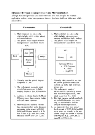
Microprocessor
Microcontroller
1. Microprocessor is a silicon chip
which includes ALU, register circuit
and control circuits.
2. The general block diagram to show
microprocessor is as shown below:
MPU
3. Normally used for general purpose
computers as CPU.
4. The performance speed, i.e. clock
speed of microprocessor is higher
ranging frequency from MHz to GHz.
5. Addition of external RAM, ROM and
I/O ports makes these systems bulkier
and much more expensive.
6. Microprocessors are more versatile
than microcontrollers as the designers
can decide on the amount of RAM,
ROM and I/O ports needed to fit the
task at hand. E.gs. Intel 8085, 8086,
Motorola 68000, Intel Core i7, etc.
1. Microcontroller is a silicon chip
which includes microprocessor,
memory and I/O in a single package.
2. The general block diagram of
microcontroller is as shown below:
MPU
Memory
I/O
Peripheral Devices
A/D Converter
Timer
Serial I/O
3. Normally microcontrollers are used
for specific purposes (embedded
system) e.g. traffic light controller,
printer, etc.
4. The performance speed of
microcontroller is relatively slower
than that of microprocessors, with
clock speed from 3-33 MHz.
5. Has fixed memory and all peripherals
are embedded together on a single
chip, so are not bulkier and are
cheaper than microprocessors.
6. As microcontrollers have already
fixed amount of RAM, ROM and I/O
ports, so are not versatile as the user
cannot change the amount of memory
and I/O ports. E.gs. AT89C51, At
mega32, AT89S52, etc.
Input
Memory
y
Output
ALU
CU
Register
Array
2. Evolution of Intel Microprocessor
4 bit Microprocessors
4004
Introduced in 1971
First microprocessor by Intel
It was a 4-bit microprocessor
Its clock speed was 740 KHz
It had 2,300 transistors
It could execute around 60,000 instructions per seconds
Used in calculators
4040
Introduced in 1974
4-bit microprocessor
3,000 transistors were used
Clock speed was 740 KHz
Interrupt features were available
8 Bit Microprocessors
8008
Introduced in 1972 it was first 8 bit microprocessor
Its clock speed was 500 KHz
Could execute 50,000 instruction per second
Used in: Computer terminals, Calculator, Bottling Machines, industrial Robots
8080
Introduced in 1974
It was also 8-bit microprocessor
Its clock speed was 2 MHz
It has 6,000 transistors
10 times faster than 8008
Could execute 500,000 instructions per second
Used In: Calculators, Industrial Robots
8085
Introduced in 1976
It was also 8-bit microprocessor
Its clock speed was 3 MHz
Its data bus is 8 bit and address bus is 16 bit
It has 6,500 transistors
It could execute 769,230 instructions per second
It could access 64KB of memory
It has 246 instructions
Used In: early PC, On-Board Instrument Data Processors
3. 16 Bit Microprocessors
8086
Introduced in 1978
First 16-bit microprocessor
Clock speed is 5 to 10 MHz
Data bus is 16-bit and address bus is 20-bit
It had 29,000 transistors
It could execute 2.5 million instructions per second
Could access 1MB of memory
It had 22,000 instructions
Used In: CPU of Microcomputers
8088
Introduced in 1979
It was also 16-bit microprocessor
It was creates as cheaper version of Intel’s 8086
16-bit processor with an 8-bit data bus
Could execute 2.5 million instructions per second
The chip become the most popular in the computer industry when IBM used it for its
first PC
80286
Introduced in 1982
It was 16-bit microprocessor
Its clock speed was 8 MHz
Data bus is 16-bit and address bus is 24-bit
Could address 16 MB of memory
It has 134,000 transistors
Could execute 4-million instructions per second
32 Bit Microprocessors
80386
Introduced in 1986
First 32-bit microprocessor
Data bus is 32 bit and address bus is 32-bit
It could address 4GB of memory
It has 275,000 transistors
Clock speed varied from 16 MHz to 33 MHz depending upon different versions
Different Versions
80386DX
80386SX
80386SL
4. 80486
Introduced in 1989
32-bit microprocessor
Had 1.2 million transistors
Clock speed varied from 16 MHz to 100 MHz depending upon the various versions
It had five different versions
80486DX
80486SX
80486DX2
80486SL
80486DX4
8KB of cache memory was introduced
Pentium
Introduced in 1993
It was also 32-bit microprocessor
Clock speed was 66 MHz
Data bus is 32-bit and address bus is 32-bit
Could address 4GB of memory
Could execute 110 million instructions per second
Cache memory
8KB for Instruction
8KB for data
Upgraded Version: Pentium Pro
Pentium II
Introduced in 1997
32-bit microprocessor
Clock speed was 233 to 450 MHz
MMX technology was supported
L2 cache and processor were on one circuit
Upgraded Version: Pentium II Xenon
Pentium III
Introduced in 1999
It was 32-bit microprocessor
Clock speed varied from 500 MHz to 1.4 GHz
It had 9.5 million transistors
Pentium IV
Introduced in 2000
32-bit microprocessor
Clock speed was from 1.3 GHz to 3.8 GHz
L1 cache was 32 KB and L2 cache was 256 KB
It had 42 million transistors
5. Intel Dual Core
Introduced in 2006
It is 32-bit or 64 bit Microprocessor
It has 2-cores
Both cores have their own internal bus and L1 cache but share the external bus and L2
cache
Support SMT (Simultaneously Multithreading Technology)
64 Bit Microprocessors
Intel Core 2
Introduced in 2006
64-bit microprocessor
Clock speed is from 1.2 GHz to 3GHz
It has 291 million transistors
L1 cache- 64 KB per core
L2 cache- 4 MB
Versions:
Intel Core 2 Duo
Intel Core 2 Quad
Intel Core 2 Extreme
Intel Core i7
Introduced in 2008
64-bit microprocessor
It has 4 physical cores
Clock speed is from 2.66 GHz to 3.33 GHz
It has 781 million transistors
L1 cache- 64 KB per core
L2 cache- 256 KB
L3 cache- 4 MB
Intel Core i5
Introduced in 2009
It is a 64-bit microprocessor
It has 4 physical cores
Its clock speed is from 2.40 GHz to 3.60 GHz
It has 781 million transistors
L1 cache- 64 KB per core
L2 cache- 256 KB
L3 cache- 8 MB
6. Intel Core i3
Introduced in 2010
64-bit microprocessor
It has 2 physical cores
Clock speed is from 2.93 GHz to 3.33 GHz
It has 781 million transistors
L1 cache- 64 KB per core
L2 cache- 512 KB
L3 cache- 4 MB
7. 8085 INTRODUCTION
The features of INTEL 8085 are:
• It is an 8 bit processor.
• It is a single chip N-MOS device with 40 pins.
• It works on 5 Volt dc power supply.
• The maximum clock frequency is 3 MHz while minimum frequency is 500 KHz.
• It provides 74 instructions with 5 different addressing modes.
• It has multiplexed address and data bus (AD0-AD7).
• It provides 16 address lines so it can access 216 =64K bytes of memory.
• It generates 8 bit I/O address so it can access 28=256 input ports.
8085 Pin Diagram
Some important pins are:
• AD0-AD7: Multiplexed Address and data lines.
• A8-A15: Tri-stated higher order address lines.
• ALE: Address latch enable is an output signal. It goes high when operation is started
by processor.
8. • S0, S1: These are the status signals used to indicate type of operation.
• ̅퐑̅̅퐃̅: Read is active low input signal used to read data from I/O device or memory.
• ̅퐖̅̅̅퐑̅: Write is an active low output signal used write data on memory or an I/O device.
• READY: This an output signal used to check the status of output device. If it is low,
μP will WAIT until it is high.
• TRAP: It is an Edge triggered highest priority, non-maskable interrupt. After TRAP,
restart occurs and execution starts from address 0024H.
• RST 5.5, 6.5, 7.5: These are maskable interrupts and have low priority than TRAP.
• ̅퐈̅퐍̅̅퐓̅̅퐑̅ & INTA: INTR is an interrupt request signal after which μP generates INTA or
interrupt acknowledge signal.
• IO/퐌̅
: This is output pin or signal used to indicate whether 8085 is working in I/O
mode (IO/M=1) or Memory mode (IO/M=0).
• HOLD & HLDA: HOLD is an input signal .When μP receives HOLD signal it
completes current machine cycle and stops executing next instruction. In response to
HOLD μP generates HLDA that is HOLD Acknowledge signal.
• ̅퐑̅̅퐄̅̅퐒̅퐄̅̅퐓̅̅퐈̅̅퐍̅: This is input signal. When RESETIN is low μp restarts and starts
executing from location 0000H.
• SID: Serial input data is input pin used to accept serial 1 bit data.
• SOD: Serial output data is output pin used to send serial 1 bit data.
• X1, X2: These are clock input signals and are connected to external LC or RC circuit.
These are divide by two so if 6 MHz is connected to X1X2, the operating frequency
becomes 3 MHz.
• VCC & VSS: Power supply VCC=+ -5Volt& VSS=-GND reference.
9. 8085 ARCHITECTURE
Fig. Block Diagram
ARITHEMATIC AND LOGIC UNIT (ALU)
Accumulator:
It is 8 bit general purpose register. It is connected to ALU. So, most of the operations
are done in Accumulator (A).
Temporary register:
It is not available for user. All the arithmetic and logical operations are done in the
temporary register but user can’t access it.
10. Flag Register: It is an 8-bit register which consists of 5 flip flops used to know status
of various operations done.
S Z - AC - P - CY
Fig. 8085 Flag Register
S: Sign flag is set when result of an operation is negative.
Z: Zero flag is set when result of an operation is 0.
AC: Auxiliary carry flag is set when there is a carry out of lower nibble or lower four
bits of the operation.
CY: Carry flag is set when there is carry generated by an operation.
P: Parity flag is set when result contains even number of 1’s.
Rest are don’t care flip flops and reserved for future use.
REGISTER ARRAY
Temporary registers (W, Z): These are not available for user. These are loaded only
when there is an operation being performed.
General purpose: There are six 8-bit general purposes register in 8085 namely B, C,
D, E, H and L. These are used for various data manipulations. They can be used in
pairs as 16-bit registers. The register pairs are: BC pair, DE pair and HL pair.
Special purpose: There are two special purpose registers in 8085:
SP (Stack Pointer): It is a 16-bit register used to hold the address of stack
during stack operation i.e PUSH and POP operations.
PC (Program Counter): It is a 16-bit register which holds the address of next
instruction to be fetched. When a single byte instruction is executed PC is
automatically incremented by 1. Upon reset PC contents are set to 0000H.
TIMIMG AND CONTROL UNIT
This unit synchronizes all the microprocessor operations with the clock and generates
the control signals necessary for communication between the microprocessor and
peripherals. The ̅푅̅̅퐷̅ and ̅푊̅̅̅푅̅ signals are sync pulse indicating the availability of data
on the data bus.
11. INSTRUCTION REGISTER AND DECODER
The instruction register and decoder are part of ALU. When an instruction is fetched
from memory, it is loaded in the instruction register. The decoder decodes the
instruction and establishes the sequence of events to flow. The instruction register is
not programmable and cannot be accessed through any instructions.
INTERRUPT CONTROL
It accepts different interrupts like TRAP, RST 5.5, RST 6.5, RST 7.5 and INTR.
INTA is interrupt acknowledgement signal.
SERIAL IO CONTROL
It is used to accept and send the serial 1 bit data by using SID and SOD signals and it
can be performed by using SIM & RIM instructions.