SlideShare a Scribd company logo
1 of 18
JFET
SMALL SIGNAL MODEL
Due to the non-linear operation
of the device, the input signal
applied can introduce amplitude
distortion at the output, if the
signal is of larger amplitude.
Hence, to maintain the response
of the amplifier as linear, the
applied input signal must be small
enough, and such operation is
called as “small signal” operation.
INTRODUCTION
• Shockley’s equation:
• The change in drain current that will result from a
change in gate-to-source voltage can be determined using
the transconductance factor (gm) in the following manner:
• The prefix ‘trans’ in the terminology applied to gm
reveals that it establishes a relationship between an
output and an input quantity (g=conductance, m=mutual).
Graphical Determination of gm
• gm is the slope of the characteristics at the point of operation.
• The slope, and therefore, gm increase
as we progress from VP to IDSS .
• As VGS approaches 0 V,
the magnitude of gm increases.
Ex:1) Determine the magnitude of gm for a JFET with
IDSS = 8 mA and VP = -4V, at the following dc bias points:
a) VGS = -0.5 V, b) VGS = -1.5 V, c) VGS = -2.5 V.
Mathematical Definition of gm
• The derivative of a function at a point is equal to the slope of
the tangent line drawn at that point.
• Plugging in VGS = 0 V into the above equation, we get the
maximum value for gm:
where the added subscript “0” indicates the value of gm when VGS = 0 V.
• In equation form,
where ‘f’ signifies forward transfer conductance and ‘s’ indicates that it is
connected to the source terminal. For JFET, gfs ranges from 1 mS to 5 mS.
Ex:2) For the JFET having the transfer characteristics
of Ex:1, a) find the maximum value of gm, b) the value
of gm at each operating point.
Plotting of VGS versus gm
• The factor [1-(VGS/VP)] is less than
unity for any value of VGS other than 0 V.
• This means that the magnitude of gm
will decrease as VGS approaches VP.
• The maximum value of gm occurs
where VGS = 0 V and the minimum
value at VGS = VP. The more negative the
value of VGS, the less the value of gm.
Plot of VGS versus gm
For the previous example:
Effect of ID on gm
• Shockley’s equation can be written in the following form :
• Substituting into the equation of gm, we get -
• gm can be determined for a few specific values of ID :
Plot of ID versus gm
The highest values of gm are obtained when
VGS approaches 0 V and ID approaches IDSS.
JFET Input Impedance (Zi)
• The input impedance of JFETs is sufficiently large, typically
above 1 GΩ. Hence, for all practical purposes, it can be
assumed that the input terminals approximate an open
circuit. Thus, in equation form,
JFET Output Impedance (Zo)
• The output admittance is indicated as “gos”or “yos”, with the
unit of µS. The typical values range between 10 μS to 50 μS.
The subscript “o” signifies output network parameter, and “s”
signifies the terminal source in the model. Therefore, output
impedance in the equation form is,
• On the characteristic curves, the output impedance is the slope
of the curve at the point of operation. The more horizontal the
curve, the greater is Zo. In the equation form,
The value of rd is
different for each
value of VGS, and
hence, rd changes
from one operating
region to the other.
• Largest value of rd
occurs for the least
value of VGS, and
hence, the smallest
value of rd occurs
when VGS = 0 V.
JFET AC Equivalent Circuit
• The input impedance is represented by the open circuit at
the input terminals, and the output impedance is
represented by the resistor “rd” from drain to source.
• At the output, the control of Id by Vgs is included as a current
source (gm.Vgs) connected from drain to source.
• The current source has its arrow pointing from drain to
source, to indicate a 180° phase shift between output and
input signals, in the common source configuration.
1. FIXED-BIAS CONFIGURATION
• C1 and C2 isolate the dc biasing arrangement from the
applied signal and the load, and they act as short circuit
equivalents for the ac analysis.
• When the values of gm & rd are determined from either the
dc biasing arrangement or the specification sheet or the
characteristic curves, the ac equivalent model of the circuit
can be substituted between the appropriate terminals.
Ex:3) The following circuit has an operating point
defined by: VGSQ= -2 V, IDQ = 5.625 mA and yos = 40 μS.
Find Zi, Zo and Av.
gm0 = (2X10m) / 8 = 2.5 mS.
gm = 2.5m (1-(2/8)) = 1.875 mS.
rd = 1/40μ = 25 kΩ.
Zi = 1 MΩ.
Zo = (25 k) ll (2 k) = 1.85 kΩ.
Av = -1.875 m X 1.85 k = -3.47.
Note: The ac analysis of self-biased JFET amplifier, with bypass
capacitor, is same as that of fixed-bias circuit.
2. VOLTAGE-DIVIDER BIAS CONFIGURATION
OF MODULE 2

More Related Content

What's hot

Dc bridge types ,derivation and its application
Dc bridge types ,derivation and its applicationDc bridge types ,derivation and its application
Dc bridge types ,derivation and its applicationkaroline Enoch
 
The complex reflection coefficient
The complex reflection coefficientThe complex reflection coefficient
The complex reflection coefficientBerkayErgn1
 
AC bridges ( Weins bridge, Desauty bridge, Maxwell's inductance bridge)
AC bridges ( Weins bridge, Desauty bridge, Maxwell's inductance bridge)AC bridges ( Weins bridge, Desauty bridge, Maxwell's inductance bridge)
AC bridges ( Weins bridge, Desauty bridge, Maxwell's inductance bridge)Eklavya Sharma
 
Lecture20 electrostatics
Lecture20 electrostaticsLecture20 electrostatics
Lecture20 electrostaticsAlex Klein
 
Inductor design
Inductor designInductor design
Inductor designbinodsahu8
 
Galvanometer,wheatstone bridge,ohm law,
Galvanometer,wheatstone bridge,ohm  law,Galvanometer,wheatstone bridge,ohm  law,
Galvanometer,wheatstone bridge,ohm law,umarjamil10000
 
Kelvin bridge and kelvin double bridge
Kelvin bridge and kelvin double bridge Kelvin bridge and kelvin double bridge
Kelvin bridge and kelvin double bridge karoline Enoch
 
Owen’s bridge and measurement of increment inductance
Owen’s bridge and measurement of increment inductanceOwen’s bridge and measurement of increment inductance
Owen’s bridge and measurement of increment inductancevishalgohel12195
 
Dc load line fixed biasing
Dc load line fixed biasingDc load line fixed biasing
Dc load line fixed biasingPRAVEENA N G
 
The Kelvin Bridge
The Kelvin  BridgeThe Kelvin  Bridge
The Kelvin BridgeSigmig
 
AC bridges: Inductance and Capacitance measurement
AC bridges: Inductance and Capacitance measurementAC bridges: Inductance and Capacitance measurement
AC bridges: Inductance and Capacitance measurementDr Naim R Kidwai
 
Schering bridge and its derivation
Schering bridge and its derivationSchering bridge and its derivation
Schering bridge and its derivationkaroline Enoch
 
Voltage series feedback
Voltage series feedbackVoltage series feedback
Voltage series feedbackPRAVEENA N G
 
Schering bridge
Schering bridge Schering bridge
Schering bridge mihir jain
 
Maxwell bridge and its types
Maxwell bridge and its types Maxwell bridge and its types
Maxwell bridge and its types karoline Enoch
 

What's hot (20)

Dc bridge types ,derivation and its application
Dc bridge types ,derivation and its applicationDc bridge types ,derivation and its application
Dc bridge types ,derivation and its application
 
MOSFET as an Amplifier
MOSFET as an AmplifierMOSFET as an Amplifier
MOSFET as an Amplifier
 
Calculated Values
Calculated ValuesCalculated Values
Calculated Values
 
The complex reflection coefficient
The complex reflection coefficientThe complex reflection coefficient
The complex reflection coefficient
 
Mosfet baising
Mosfet baisingMosfet baising
Mosfet baising
 
AC bridges ( Weins bridge, Desauty bridge, Maxwell's inductance bridge)
AC bridges ( Weins bridge, Desauty bridge, Maxwell's inductance bridge)AC bridges ( Weins bridge, Desauty bridge, Maxwell's inductance bridge)
AC bridges ( Weins bridge, Desauty bridge, Maxwell's inductance bridge)
 
Lecture20 electrostatics
Lecture20 electrostaticsLecture20 electrostatics
Lecture20 electrostatics
 
Inductor design
Inductor designInductor design
Inductor design
 
Galvanometer,wheatstone bridge,ohm law,
Galvanometer,wheatstone bridge,ohm  law,Galvanometer,wheatstone bridge,ohm  law,
Galvanometer,wheatstone bridge,ohm law,
 
Chapter 6
Chapter 6Chapter 6
Chapter 6
 
Kelvin bridge and kelvin double bridge
Kelvin bridge and kelvin double bridge Kelvin bridge and kelvin double bridge
Kelvin bridge and kelvin double bridge
 
Owen’s bridge and measurement of increment inductance
Owen’s bridge and measurement of increment inductanceOwen’s bridge and measurement of increment inductance
Owen’s bridge and measurement of increment inductance
 
Dc load line fixed biasing
Dc load line fixed biasingDc load line fixed biasing
Dc load line fixed biasing
 
The Kelvin Bridge
The Kelvin  BridgeThe Kelvin  Bridge
The Kelvin Bridge
 
Gauss LAW
Gauss LAWGauss LAW
Gauss LAW
 
AC bridges: Inductance and Capacitance measurement
AC bridges: Inductance and Capacitance measurementAC bridges: Inductance and Capacitance measurement
AC bridges: Inductance and Capacitance measurement
 
Schering bridge and its derivation
Schering bridge and its derivationSchering bridge and its derivation
Schering bridge and its derivation
 
Voltage series feedback
Voltage series feedbackVoltage series feedback
Voltage series feedback
 
Schering bridge
Schering bridge Schering bridge
Schering bridge
 
Maxwell bridge and its types
Maxwell bridge and its types Maxwell bridge and its types
Maxwell bridge and its types
 

Similar to Analog Electronic Circuits - Module 2.3

Chapter 4 semiconductor devicee JFET.pdf
Chapter 4 semiconductor devicee JFET.pdfChapter 4 semiconductor devicee JFET.pdf
Chapter 4 semiconductor devicee JFET.pdfYohannes427126
 
(Latest) topic 5 field_effect_transistors
(Latest) topic 5 field_effect_transistors(Latest) topic 5 field_effect_transistors
(Latest) topic 5 field_effect_transistorsGabriel O'Brien
 
Jfet( voltage divider bias ) sheraz
Jfet( voltage divider bias ) sherazJfet( voltage divider bias ) sheraz
Jfet( voltage divider bias ) sherazSheeraz Ahmed
 
note_1474205380.pdf
note_1474205380.pdfnote_1474205380.pdf
note_1474205380.pdfGunaG14
 
Transistor Amplifiers 2.pptx
Transistor Amplifiers 2.pptxTransistor Amplifiers 2.pptx
Transistor Amplifiers 2.pptxJbmulindwa
 
Grid tie inverter
Grid tie inverterGrid tie inverter
Grid tie inverterNitesh Jha
 
Design of up converter at 2.4GHz using Analog VLSI with 22nm Technology
Design of up converter at 2.4GHz using Analog VLSI with 22nm TechnologyDesign of up converter at 2.4GHz using Analog VLSI with 22nm Technology
Design of up converter at 2.4GHz using Analog VLSI with 22nm Technologyijsrd.com
 
Mosfet on and off time.pdf
Mosfet on and off time.pdfMosfet on and off time.pdf
Mosfet on and off time.pdfIsiMiyake
 
CMOS analog IC Design presentation.pptx
CMOS analog IC Design presentation.pptxCMOS analog IC Design presentation.pptx
CMOS analog IC Design presentation.pptxAkash588342
 
Analog Electronic Circuits - Module 2.2
Analog Electronic Circuits - Module 2.2Analog Electronic Circuits - Module 2.2
Analog Electronic Circuits - Module 2.2Aravinda Koithyar
 
Ixan0010 drivers igbt
Ixan0010 drivers igbtIxan0010 drivers igbt
Ixan0010 drivers igbtDario Delgado
 
APPLICATIONS OF FLOATING-GATE MOSFET IN THE DESIGN OF INVERTER AND RING OSCIL...
APPLICATIONS OF FLOATING-GATE MOSFET IN THE DESIGN OF INVERTER AND RING OSCIL...APPLICATIONS OF FLOATING-GATE MOSFET IN THE DESIGN OF INVERTER AND RING OSCIL...
APPLICATIONS OF FLOATING-GATE MOSFET IN THE DESIGN OF INVERTER AND RING OSCIL...elelijjournal
 
single stage amplifier Unit 5 AMVLSI
single stage amplifier Unit 5 AMVLSIsingle stage amplifier Unit 5 AMVLSI
single stage amplifier Unit 5 AMVLSIHarsha Raju
 
Operational Amplifier Design
Operational Amplifier DesignOperational Amplifier Design
Operational Amplifier DesignBharat Biyani
 
Lect2 up190 (100327)
Lect2 up190 (100327)Lect2 up190 (100327)
Lect2 up190 (100327)aicdesign
 
FET lecture_Electronics by Arif Sir
FET lecture_Electronics by Arif SirFET lecture_Electronics by Arif Sir
FET lecture_Electronics by Arif SirMuntasir Mahdi
 

Similar to Analog Electronic Circuits - Module 2.3 (20)

FET AMPLIFIER
FET AMPLIFIERFET AMPLIFIER
FET AMPLIFIER
 
Chapter 4 semiconductor devicee JFET.pdf
Chapter 4 semiconductor devicee JFET.pdfChapter 4 semiconductor devicee JFET.pdf
Chapter 4 semiconductor devicee JFET.pdf
 
(Latest) topic 5 field_effect_transistors
(Latest) topic 5 field_effect_transistors(Latest) topic 5 field_effect_transistors
(Latest) topic 5 field_effect_transistors
 
Jfet( voltage divider bias ) sheraz
Jfet( voltage divider bias ) sherazJfet( voltage divider bias ) sheraz
Jfet( voltage divider bias ) sheraz
 
note_1474205380.pdf
note_1474205380.pdfnote_1474205380.pdf
note_1474205380.pdf
 
Transistor Amplifiers 2.pptx
Transistor Amplifiers 2.pptxTransistor Amplifiers 2.pptx
Transistor Amplifiers 2.pptx
 
MOSFETs
MOSFETsMOSFETs
MOSFETs
 
Grid tie inverter
Grid tie inverterGrid tie inverter
Grid tie inverter
 
MOSFET.pptx
MOSFET.pptxMOSFET.pptx
MOSFET.pptx
 
Design of up converter at 2.4GHz using Analog VLSI with 22nm Technology
Design of up converter at 2.4GHz using Analog VLSI with 22nm TechnologyDesign of up converter at 2.4GHz using Analog VLSI with 22nm Technology
Design of up converter at 2.4GHz using Analog VLSI with 22nm Technology
 
Mosfet on and off time.pdf
Mosfet on and off time.pdfMosfet on and off time.pdf
Mosfet on and off time.pdf
 
CMOS analog IC Design presentation.pptx
CMOS analog IC Design presentation.pptxCMOS analog IC Design presentation.pptx
CMOS analog IC Design presentation.pptx
 
Analog Electronic Circuits - Module 2.2
Analog Electronic Circuits - Module 2.2Analog Electronic Circuits - Module 2.2
Analog Electronic Circuits - Module 2.2
 
Ixan0010 drivers igbt
Ixan0010 drivers igbtIxan0010 drivers igbt
Ixan0010 drivers igbt
 
APPLICATIONS OF FLOATING-GATE MOSFET IN THE DESIGN OF INVERTER AND RING OSCIL...
APPLICATIONS OF FLOATING-GATE MOSFET IN THE DESIGN OF INVERTER AND RING OSCIL...APPLICATIONS OF FLOATING-GATE MOSFET IN THE DESIGN OF INVERTER AND RING OSCIL...
APPLICATIONS OF FLOATING-GATE MOSFET IN THE DESIGN OF INVERTER AND RING OSCIL...
 
single stage amplifier Unit 5 AMVLSI
single stage amplifier Unit 5 AMVLSIsingle stage amplifier Unit 5 AMVLSI
single stage amplifier Unit 5 AMVLSI
 
FET (Field Effect Transistors)
FET (Field Effect Transistors)FET (Field Effect Transistors)
FET (Field Effect Transistors)
 
Operational Amplifier Design
Operational Amplifier DesignOperational Amplifier Design
Operational Amplifier Design
 
Lect2 up190 (100327)
Lect2 up190 (100327)Lect2 up190 (100327)
Lect2 up190 (100327)
 
FET lecture_Electronics by Arif Sir
FET lecture_Electronics by Arif SirFET lecture_Electronics by Arif Sir
FET lecture_Electronics by Arif Sir
 

More from Aravinda Koithyar

More from Aravinda Koithyar (20)

Analog Electronic Circuits - Module 5
Analog Electronic Circuits - Module 5Analog Electronic Circuits - Module 5
Analog Electronic Circuits - Module 5
 
Analog Electronic Circuits - Module 4
Analog Electronic Circuits - Module 4Analog Electronic Circuits - Module 4
Analog Electronic Circuits - Module 4
 
Analog Electronic Circuits - Module 3
Analog Electronic Circuits - Module 3Analog Electronic Circuits - Module 3
Analog Electronic Circuits - Module 3
 
Analog Electronic Circuits - Module 2.1
Analog Electronic Circuits - Module 2.1Analog Electronic Circuits - Module 2.1
Analog Electronic Circuits - Module 2.1
 
System design using HDL - Module 1
System design using HDL - Module 1System design using HDL - Module 1
System design using HDL - Module 1
 
System design using HDL - Module 5
System design using HDL - Module 5System design using HDL - Module 5
System design using HDL - Module 5
 
System design using HDL - Module 2
System design using HDL - Module 2System design using HDL - Module 2
System design using HDL - Module 2
 
System design using HDL - Module 3
System design using HDL - Module 3System design using HDL - Module 3
System design using HDL - Module 3
 
Spiritual health through yoga
Spiritual health through yogaSpiritual health through yoga
Spiritual health through yoga
 
Lessons of leadership
Lessons of leadershipLessons of leadership
Lessons of leadership
 
Great sayings
Great sayingsGreat sayings
Great sayings
 
Sanskrit words with pictures
Sanskrit words with picturesSanskrit words with pictures
Sanskrit words with pictures
 
Guru and Gaayathree
Guru and GaayathreeGuru and Gaayathree
Guru and Gaayathree
 
Samskrtha Pravesha
Samskrtha PraveshaSamskrtha Pravesha
Samskrtha Pravesha
 
Adi shankara's literary works
Adi shankara's literary worksAdi shankara's literary works
Adi shankara's literary works
 
Introduction to yoga
Introduction to yogaIntroduction to yoga
Introduction to yoga
 
Pranayama
PranayamaPranayama
Pranayama
 
Sacred secret
Sacred secretSacred secret
Sacred secret
 
Memory
MemoryMemory
Memory
 
Vision & mouth fitness
Vision & mouth fitnessVision & mouth fitness
Vision & mouth fitness
 

Recently uploaded

What are the advantages and disadvantages of membrane structures.pptx
What are the advantages and disadvantages of membrane structures.pptxWhat are the advantages and disadvantages of membrane structures.pptx
What are the advantages and disadvantages of membrane structures.pptxwendy cai
 
EduAI - E learning Platform integrated with AI
EduAI - E learning Platform integrated with AIEduAI - E learning Platform integrated with AI
EduAI - E learning Platform integrated with AIkoyaldeepu123
 
Heart Disease Prediction using machine learning.pptx
Heart Disease Prediction using machine learning.pptxHeart Disease Prediction using machine learning.pptx
Heart Disease Prediction using machine learning.pptxPoojaBan
 
main PPT.pptx of girls hostel security using rfid
main PPT.pptx of girls hostel security using rfidmain PPT.pptx of girls hostel security using rfid
main PPT.pptx of girls hostel security using rfidNikhilNagaraju
 
complete construction, environmental and economics information of biomass com...
complete construction, environmental and economics information of biomass com...complete construction, environmental and economics information of biomass com...
complete construction, environmental and economics information of biomass com...asadnawaz62
 
Biology for Computer Engineers Course Handout.pptx
Biology for Computer Engineers Course Handout.pptxBiology for Computer Engineers Course Handout.pptx
Biology for Computer Engineers Course Handout.pptxDeepakSakkari2
 
Oxy acetylene welding presentation note.
Oxy acetylene welding presentation note.Oxy acetylene welding presentation note.
Oxy acetylene welding presentation note.eptoze12
 
UNIT III ANALOG ELECTRONICS (BASIC ELECTRONICS)
UNIT III ANALOG ELECTRONICS (BASIC ELECTRONICS)UNIT III ANALOG ELECTRONICS (BASIC ELECTRONICS)
UNIT III ANALOG ELECTRONICS (BASIC ELECTRONICS)Dr SOUNDIRARAJ N
 
Introduction to Machine Learning Unit-3 for II MECH
Introduction to Machine Learning Unit-3 for II MECHIntroduction to Machine Learning Unit-3 for II MECH
Introduction to Machine Learning Unit-3 for II MECHC Sai Kiran
 
Effects of rheological properties on mixing
Effects of rheological properties on mixingEffects of rheological properties on mixing
Effects of rheological properties on mixingviprabot1
 
Arduino_CSE ece ppt for working and principal of arduino.ppt
Arduino_CSE ece ppt for working and principal of arduino.pptArduino_CSE ece ppt for working and principal of arduino.ppt
Arduino_CSE ece ppt for working and principal of arduino.pptSAURABHKUMAR892774
 
An experimental study in using natural admixture as an alternative for chemic...
An experimental study in using natural admixture as an alternative for chemic...An experimental study in using natural admixture as an alternative for chemic...
An experimental study in using natural admixture as an alternative for chemic...Chandu841456
 
Artificial-Intelligence-in-Electronics (K).pptx
Artificial-Intelligence-in-Electronics (K).pptxArtificial-Intelligence-in-Electronics (K).pptx
Artificial-Intelligence-in-Electronics (K).pptxbritheesh05
 
Risk Assessment For Installation of Drainage Pipes.pdf
Risk Assessment For Installation of Drainage Pipes.pdfRisk Assessment For Installation of Drainage Pipes.pdf
Risk Assessment For Installation of Drainage Pipes.pdfROCENODodongVILLACER
 
Call Us ≽ 8377877756 ≼ Call Girls In Shastri Nagar (Delhi)
Call Us ≽ 8377877756 ≼ Call Girls In Shastri Nagar (Delhi)Call Us ≽ 8377877756 ≼ Call Girls In Shastri Nagar (Delhi)
Call Us ≽ 8377877756 ≼ Call Girls In Shastri Nagar (Delhi)dollysharma2066
 
Electronically Controlled suspensions system .pdf
Electronically Controlled suspensions system .pdfElectronically Controlled suspensions system .pdf
Electronically Controlled suspensions system .pdfme23b1001
 

Recently uploaded (20)

Design and analysis of solar grass cutter.pdf
Design and analysis of solar grass cutter.pdfDesign and analysis of solar grass cutter.pdf
Design and analysis of solar grass cutter.pdf
 
POWER SYSTEMS-1 Complete notes examples
POWER SYSTEMS-1 Complete notes  examplesPOWER SYSTEMS-1 Complete notes  examples
POWER SYSTEMS-1 Complete notes examples
 
What are the advantages and disadvantages of membrane structures.pptx
What are the advantages and disadvantages of membrane structures.pptxWhat are the advantages and disadvantages of membrane structures.pptx
What are the advantages and disadvantages of membrane structures.pptx
 
EduAI - E learning Platform integrated with AI
EduAI - E learning Platform integrated with AIEduAI - E learning Platform integrated with AI
EduAI - E learning Platform integrated with AI
 
Heart Disease Prediction using machine learning.pptx
Heart Disease Prediction using machine learning.pptxHeart Disease Prediction using machine learning.pptx
Heart Disease Prediction using machine learning.pptx
 
main PPT.pptx of girls hostel security using rfid
main PPT.pptx of girls hostel security using rfidmain PPT.pptx of girls hostel security using rfid
main PPT.pptx of girls hostel security using rfid
 
complete construction, environmental and economics information of biomass com...
complete construction, environmental and economics information of biomass com...complete construction, environmental and economics information of biomass com...
complete construction, environmental and economics information of biomass com...
 
Exploring_Network_Security_with_JA3_by_Rakesh Seal.pptx
Exploring_Network_Security_with_JA3_by_Rakesh Seal.pptxExploring_Network_Security_with_JA3_by_Rakesh Seal.pptx
Exploring_Network_Security_with_JA3_by_Rakesh Seal.pptx
 
Biology for Computer Engineers Course Handout.pptx
Biology for Computer Engineers Course Handout.pptxBiology for Computer Engineers Course Handout.pptx
Biology for Computer Engineers Course Handout.pptx
 
Oxy acetylene welding presentation note.
Oxy acetylene welding presentation note.Oxy acetylene welding presentation note.
Oxy acetylene welding presentation note.
 
UNIT III ANALOG ELECTRONICS (BASIC ELECTRONICS)
UNIT III ANALOG ELECTRONICS (BASIC ELECTRONICS)UNIT III ANALOG ELECTRONICS (BASIC ELECTRONICS)
UNIT III ANALOG ELECTRONICS (BASIC ELECTRONICS)
 
Introduction to Machine Learning Unit-3 for II MECH
Introduction to Machine Learning Unit-3 for II MECHIntroduction to Machine Learning Unit-3 for II MECH
Introduction to Machine Learning Unit-3 for II MECH
 
Effects of rheological properties on mixing
Effects of rheological properties on mixingEffects of rheological properties on mixing
Effects of rheological properties on mixing
 
Arduino_CSE ece ppt for working and principal of arduino.ppt
Arduino_CSE ece ppt for working and principal of arduino.pptArduino_CSE ece ppt for working and principal of arduino.ppt
Arduino_CSE ece ppt for working and principal of arduino.ppt
 
An experimental study in using natural admixture as an alternative for chemic...
An experimental study in using natural admixture as an alternative for chemic...An experimental study in using natural admixture as an alternative for chemic...
An experimental study in using natural admixture as an alternative for chemic...
 
Artificial-Intelligence-in-Electronics (K).pptx
Artificial-Intelligence-in-Electronics (K).pptxArtificial-Intelligence-in-Electronics (K).pptx
Artificial-Intelligence-in-Electronics (K).pptx
 
Risk Assessment For Installation of Drainage Pipes.pdf
Risk Assessment For Installation of Drainage Pipes.pdfRisk Assessment For Installation of Drainage Pipes.pdf
Risk Assessment For Installation of Drainage Pipes.pdf
 
Call Us ≽ 8377877756 ≼ Call Girls In Shastri Nagar (Delhi)
Call Us ≽ 8377877756 ≼ Call Girls In Shastri Nagar (Delhi)Call Us ≽ 8377877756 ≼ Call Girls In Shastri Nagar (Delhi)
Call Us ≽ 8377877756 ≼ Call Girls In Shastri Nagar (Delhi)
 
young call girls in Rajiv Chowk🔝 9953056974 🔝 Delhi escort Service
young call girls in Rajiv Chowk🔝 9953056974 🔝 Delhi escort Serviceyoung call girls in Rajiv Chowk🔝 9953056974 🔝 Delhi escort Service
young call girls in Rajiv Chowk🔝 9953056974 🔝 Delhi escort Service
 
Electronically Controlled suspensions system .pdf
Electronically Controlled suspensions system .pdfElectronically Controlled suspensions system .pdf
Electronically Controlled suspensions system .pdf
 

Analog Electronic Circuits - Module 2.3

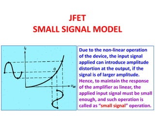
  • 1. JFET SMALL SIGNAL MODEL Due to the non-linear operation of the device, the input signal applied can introduce amplitude distortion at the output, if the signal is of larger amplitude. Hence, to maintain the response of the amplifier as linear, the applied input signal must be small enough, and such operation is called as “small signal” operation.
  • 2. INTRODUCTION • Shockley’s equation: • The change in drain current that will result from a change in gate-to-source voltage can be determined using the transconductance factor (gm) in the following manner: • The prefix ‘trans’ in the terminology applied to gm reveals that it establishes a relationship between an output and an input quantity (g=conductance, m=mutual).
  • 3. Graphical Determination of gm • gm is the slope of the characteristics at the point of operation. • The slope, and therefore, gm increase as we progress from VP to IDSS . • As VGS approaches 0 V, the magnitude of gm increases.
  • 4. Ex:1) Determine the magnitude of gm for a JFET with IDSS = 8 mA and VP = -4V, at the following dc bias points: a) VGS = -0.5 V, b) VGS = -1.5 V, c) VGS = -2.5 V.
  • 5. Mathematical Definition of gm • The derivative of a function at a point is equal to the slope of the tangent line drawn at that point.
  • 6. • Plugging in VGS = 0 V into the above equation, we get the maximum value for gm: where the added subscript “0” indicates the value of gm when VGS = 0 V. • In equation form, where ‘f’ signifies forward transfer conductance and ‘s’ indicates that it is connected to the source terminal. For JFET, gfs ranges from 1 mS to 5 mS.
  • 7. Ex:2) For the JFET having the transfer characteristics of Ex:1, a) find the maximum value of gm, b) the value of gm at each operating point.
  • 8. Plotting of VGS versus gm • The factor [1-(VGS/VP)] is less than unity for any value of VGS other than 0 V. • This means that the magnitude of gm will decrease as VGS approaches VP. • The maximum value of gm occurs where VGS = 0 V and the minimum value at VGS = VP. The more negative the value of VGS, the less the value of gm. Plot of VGS versus gm For the previous example:
  • 9. Effect of ID on gm • Shockley’s equation can be written in the following form : • Substituting into the equation of gm, we get - • gm can be determined for a few specific values of ID :
  • 10. Plot of ID versus gm The highest values of gm are obtained when VGS approaches 0 V and ID approaches IDSS.
  • 11. JFET Input Impedance (Zi) • The input impedance of JFETs is sufficiently large, typically above 1 GΩ. Hence, for all practical purposes, it can be assumed that the input terminals approximate an open circuit. Thus, in equation form, JFET Output Impedance (Zo) • The output admittance is indicated as “gos”or “yos”, with the unit of µS. The typical values range between 10 μS to 50 μS. The subscript “o” signifies output network parameter, and “s” signifies the terminal source in the model. Therefore, output impedance in the equation form is,
  • 12. • On the characteristic curves, the output impedance is the slope of the curve at the point of operation. The more horizontal the curve, the greater is Zo. In the equation form, The value of rd is different for each value of VGS, and hence, rd changes from one operating region to the other. • Largest value of rd occurs for the least value of VGS, and hence, the smallest value of rd occurs when VGS = 0 V.
  • 13. JFET AC Equivalent Circuit • The input impedance is represented by the open circuit at the input terminals, and the output impedance is represented by the resistor “rd” from drain to source. • At the output, the control of Id by Vgs is included as a current source (gm.Vgs) connected from drain to source. • The current source has its arrow pointing from drain to source, to indicate a 180° phase shift between output and input signals, in the common source configuration.
  • 14. 1. FIXED-BIAS CONFIGURATION • C1 and C2 isolate the dc biasing arrangement from the applied signal and the load, and they act as short circuit equivalents for the ac analysis. • When the values of gm & rd are determined from either the dc biasing arrangement or the specification sheet or the characteristic curves, the ac equivalent model of the circuit can be substituted between the appropriate terminals.
  • 15.
  • 16. Ex:3) The following circuit has an operating point defined by: VGSQ= -2 V, IDQ = 5.625 mA and yos = 40 μS. Find Zi, Zo and Av. gm0 = (2X10m) / 8 = 2.5 mS. gm = 2.5m (1-(2/8)) = 1.875 mS. rd = 1/40μ = 25 kΩ. Zi = 1 MΩ. Zo = (25 k) ll (2 k) = 1.85 kΩ. Av = -1.875 m X 1.85 k = -3.47. Note: The ac analysis of self-biased JFET amplifier, with bypass capacitor, is same as that of fixed-bias circuit.
  • 17. 2. VOLTAGE-DIVIDER BIAS CONFIGURATION