MANUFACTURING PROCESS-II UNIT-1 THEORY OF METAL CUTTING
Solar Cells.pptx
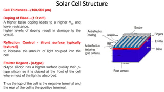
1. Solar Cell Structure
Cell Thickness - (100-500 µm)
Doping of Base - (1 Ω·cm)
A higher base doping leads to a higher Voc and
lower resistance,
higher levels of doping result in damage to the
crystal.
Reflection Control - (front surface typically
textured)
to increase the amount of light coupled into the
cell.
Emitter Dopant - (n-type)
N-type silicon has a higher surface quality than p-
type silicon so it is placed at the front of the cell
where most of the light is absorbed.
Thus the top of the cell is the negative terminal and
the rear of the cell is the positive terminal.
2. Silicon
• Si – mainly in the form of oxide of
Si, SiO2.
• Found in the form of quartz, sand
silicates.
• Naturally occurring quartz –
impurities – Al, B, P, Cu, C, Ca, Mg,
Fe Mn, etc.
• Impurities removed – solar cell
applications or electronics
applications.
• Acceptable impurity range – parts
per billion (ppb) – Electronic
application
• Parts per million – solar cell
• Si atomic density – 5 *1022
atoms/cm3.
• ppb – 5*1013 impurity atoms/cm3 in
Si.
• ppm – 5 *1016 impurity atoms/cm3
in Si .
3. Solar cell Structure
Emitter Thickness - (<1 μm)
A large fraction of light is absorbed close to the front surface. By making the front layer
very thin, a large fraction of the carriers generated by the incoming light are created
within a diffusion length of the p-n junction.
Doping Level of Emitter - (100 Ω/cm-3)
The front junction is doped to a level sufficient to conduct away the generated
electricity without resistive loses. However, excessive levels of doping reduces the
material's quality to the extent that carriers recombine before reaching the junction.
Grid Pattern. - (fingers 20 to 200 µm width, placed 1 - 5 mm apart)
The resistivity of silicon is too high to conduct away all the current generated, so a
lower resistivity metal grid is placed on the surface to conduct away the current
Rear Contact.
Does not need to be transparent. The design of the rear contact is becoming
increasingly important as overall efficiency increases and the cells become thinner.
4. Refining Silicon
• The oxygen is removed to produce metallurgical grade silicon – 98%
pure.
• It is further refined to produce electronic grade silicon.
• An intermediate grade with impurity levels between metallurgical silicon
and semiconductor grade silicon is often termed solar grade silicon.
• Metallurgical Grade Silicon
• The silica is reduced (oxygen removed) through a reaction with carbon
in the form of coal, charcoal and heating to 1500-2000 °C in an
electrode arc furnace.
• SiO2 + C → Si + CO2
• The resulting silicon is metallurgical grade silicon (MG-Si). It is 98%
pure and is used extensively in the metallurgical industry.
5. How is Metallurgical Si Made?
• Reduction of quartz in a submerged electric arc furnace. Highly energy intensive process.
Large plants. A medium sized EAF has a crucible diameter of 7 m, graphite electrodes each
15 m tall, weighing 20 tons each.
6.
7. Metallurgical Grade Silicon
• Metallurgical (MG) silicon is 98–99% pure, with a major
contamination of carbon, alkali-earth and transition metals.
• The transition metals in the silicon result in deep levels in the
bandgap and the high recombination activity make
metallurgical grade silicon unsuitable for use in electronics.
• In addition, boron and phosphorus dopant impurities are much too
high in concentration (>50–100 ppmw) to allow suitable
compensation procedures
8. Electronic Grade Silicon
• Powdered MG-Si is reacted with anhydrous HCl at 300 °C in a
fluidized bed reactor to form SiHCl3
• Si + 3HCl → SiHCl3 + H2
• During this reaction impurities such as Fe, Al, and B react to
form their halides (e.g. FeCl3, AlCl3, and BCl3).
• The SiHCl3 has a low boiling point of 31.8 °C and distillation is
used to purify the SiHCl3 from the impurity halides.
• The resulting SiHCl3 now has electrically active impurities(such
as Al, P, B, Fe, Cu or Au) of less than 1 parts per billion atom.
9. Electronic Grade Silicon
• Finally, the pure SiHCl3 is reacted with hydrogen at 1100°C for ~200 –
300 hours to produce a very pure form of silicon.
• SiHCl3 + H2 →Si + 3 HCl
• The reaction takes place inside large vacuum chambers and the
silicon is deposited onto thin polysilicon rods (small grain size silicon)
to produce high-purity polysilicon rods of diameter 150-200mm.
• The process was first developed by Siemens in the 60's and is often
referred to as the Siemens process.
• The resulting rods of semiconductor grade silicon are broken up to
form the feedstock for the crystallisation process.
10. Crystalline Silicon Solar Cells
Descriptor Symbol Grain Size
Common Growth
Techniques
Single crystal
sc-Si >10cm
Czochralski (CZ) float zone
(FZ)
Multicrystalline mc-Si 1mm-10cm Cast, sheet, ribbon
Polycrystalline pc-Si 1µm-1mm
Chemical-vapour
deposition
Microcrystalline µc-Si <1µm Plasma deposition