SlideShare a Scribd company logo
1 of 4
Download to read offline
Continued on next page
The transistor enabled the electronic func-
tions of modulation and amplification to be
performed in a tiny piece of silicon, which
consumed a fraction of the power used by
vacuum tube based electronics, and ush-
ered in the era of solid-state electronics
exemplified by the popular transistor radio
of the 1950s.
The integrated circuit derived from the
development of the planar silicon process,
which permitted simultaneous fabrication of
multiple transistors and other electronic
components in the surface of a silicon
wafer. The individual components could
then be interconnected on the surface of the
chip to produce functional semiconductor
devices, such as memories and micro-
processors. These devices enabled the per-
sonal computer revolution, along with the
plethora of electronic equipment exempli-
fied by cell phones, digital cameras and
such like that today constitute a near trillion
dollar electronics market, sustained by a
$150B market for semiconductors.
Since its inception circa 1960, the modern
semiconductor industry has been driven for
reasons of economics, speed and reliability
to build more and more functionality into
the integrated circuit or ‘chip’. The princi-
pal means to accomplish this has been to
shrink the size of the individual circuit ele-
ments. By reducing the feature size associ-
ated with the circuit elements of the transis-
tors in a memory cell, for example, smaller
and smaller transistors can be fabricated
enabling more of them to be packed into a
given area of silicon real estate, thereby
increasing functionality while lowering the
cost of a memory ‘bit’. Since 1960, the
cost of a transistor has fallen by a factor of
107, which is a triumph of technology
matched by few other advances.
Shrinking the size of circuit elements, e.g.,
the gate feature of a transistor, also enables
the transistor to operate at faster speed,
thereby reducing the time required to per-
form certain operations. The 2.2 GHz
speed of a Pentium 4 processor, for exam-
ple, compared with 66 MHz of the earlier
generation Pentium 1 derives primarily from
the much smaller gate dimensions of the for-
mer. The third advantage attending shrink-
age of the device is reliability. Being able
to cram 1GByte of memory, for example,
into a single chip results in a more reliable
package than having to interconnect and
package 4 separate 256MByte chips.
These advantages provide a clear incentive
to chip manufacturers to shrink the feature
size as quickly as possible to gain competi-
tive advantage by bringing the latest gener-
ation in chip design to market before their
competitors. But how quickly?
Historically, the industry has been able to
double the number of transistors on a chip
approximately every 18 months. This trend
was actually first reported by Gordon
Moore in 1965 in a review article pub-
lished in Electronics. Moore who, subse-
Moore’s Law and the
Technology S-Curve
The birth of the modern electronics industry can be traced to two seminal inventions - the invention of the transis-
tor in 1948 at AT&T’s Bell Telephone Laboratories in New Jersey in 1948, and the invention of the integrated cir-
cuit in 1959 by Robert Noyce at
Fairchild and (independently) Jack
Kilby at Texas Instruments.
by Murrae J. Bowden
FIGURE 1. Moore’s Law
WINTER 2004
ISSUE 1
VOLUME 8
SATMS T E V E N S A L L I A N C E F O R T E C H N O L O G Y M A N A G E M E N T
CurrentIssuesin
TechnologyManagement
quently cofounded Intel along with Robert
Noyce, noted that the number of transistors
on a silicon chip, plotted as a semi log plot
against time, had increased linearly over
the preceding 5 years, doubling approxi-
mately every 18 months. Moore reasoned
that continued improvements in manufactur-
ing technology, innovation (device design)
and chip size should enable that trend to
continue for several more years. Just how
well Moore predicted the industry trend can
be seen in Figure 1, which shows a semi-
log plot of the number of transistors in the
various generations of microprocessor chips
against time through 2000 indicating con-
tinuation of the linear trend for the past 35
years!
So accurate was Moore’s prediction, it has
become enshrined in the industry lore as
Moore’s Law, and subsequently codified as
the International Road Map for
Semiconductors. For forty years, Moore’s
Law has been the yardstick driving innova-
tion as semiconductor manufacturers contin-
ually strove to gain competitive advantage
by being first to market at the next technolo-
gy node within the time frame ‘specified’
by Moore’s Law, or even earlier. Indeed,
‘beat Moore’s Law’ has become the com-
petitive mantra for leading-edge firms.
Moore’s Law is an example of a classic S-
curve whereby performance as measured
by some convenient metric, e.g., speed,
plotted on a linear scale follows the shape
of an S over time, ultimately reaching a
limit determined by some fundamental phys-
ical constraint associated with the underly-
ing technology, such as a basic law of
physics (Figure 2). At this point, the tech-
nology is mature with no potential for fur-
ther improvement.
To understand how the industry has been
able to adhere to the trajectory of Moore’s
Law, it will be helpful to have an under-
standing of the underlying technologies
used to manufacture integrated circuits.
Principal among these is optical lithogra-
phy, shown schematically in Figure 3.
A silicon wafer is first oxidized to create a
thin film of silicon dioxide on the surface of
the wafer. The wafer is then coated with a
thin film of a photosensitive material called
a photoresist, and exposed to a patterned
source of radiation (by means of a pho-
tomask) to form a latent image of the mask
pattern in the photoresist. Development of
that latent image creates a three-dimension-
al replica of the two-dimensional mask pat-
tern in the photoresist. The process is analo-
gous to photography with the exposure tool
equivalent to the camera, and the photore-
sist equivalent to the photographic film.
Etching the oxide layer bares the silicon
substrate, enabling subsequent modification
of the electrical properties in these precisely
patterned areas.
As seen in Figure 3, there are two critical
requirements associated with the lithograph-
ic process - tools to translate the circuit
image into a spatially modulated aerial
image, and resist materials to record that
image as a latent image, which can subse-
quently be developed to form a three-
dimensional pattern in the resist film. Both
are highly interdependent. Development of
a suitable resist requires tailoring the photo-
chemistry of the resist to the wavelength
associated with the exposure tool, and
development of the tool requires availability
of a suitable photoresist. Both exposure tool
and resist must be commercially available
to the chip manufacturer in the timeframe
"dictated" by Moore’s Law.
The problem is that the development of
viable lithographic tools and process tech-
nologies takes a considerable period of
time - typically10 years and more, which
means that technology choices must be
made long before the extant technology
has matured. Why should this be a prob-
lem?
In the early 1970s, technologists believed,
based on prevailing knowledge of physics
and materials science, that diffraction/engi-
neering constraints would limit the resolu-
tion of optical lithography to around 2.0
micro meters (µm). Hence, practical realiza-
tion of Moore’s Law beyond feature sizes of
2.0µm would require development of an
alternative exposure technology offering
Continued on next page
FIGURE 2. Technology S-curve
FIGURE 3. Lithographic Fabrication Scheme
higher resolution. Although the optical per-
formance "limit" was not anticipated for
several more years, early choice and devel-
opment of a substitute technology was
needed in order to assure timely availability
of the next generation of manufacturing
technology. In response, advanced R&D
organizations, such as Bell Labs, IBM,
Texas Instruments, Hitachi, and others
began around 1970 to pour millions of dol-
lars into the development of electron beam
lithography, which was seen as the logical
successor to optical lithography.
Committing to a successor technology and
development timeframe long before the
extant technology has matured carries enor-
mous risk. Factors include:
• The correctness of the assessment of
the performance limit associated with
the prevailing technology
• Potential for development of sustain-
ing technologies enabling further pro-
gression along the technology S-curve,
i.e., the predicted performance limit
derives from engineering limitations of
the prevailing technology, not with the
larger optical lithography paradigm
• The technical and economic viability of
the substitute technology
Failure to adequately consider these risks
may result in flawed technology strategies
and business decisions that can threaten the
viability of the business.
In the case of optical lithography, the pre-
diction of 2.0µm as the performance limit
proved completely wrong. Subsequent
improvements in sustaining technologies
associated with optical lithography, espe-
cially the development of reduction step-
and-repeat printing tools employing shorter
and shorter wavelengths, enabled printing
of circuit features well below 2.0µm.
However, this was not before millions and
millions of dollars had been spent on devel-
oping scanning electron beam exposure
tools, that subsequently came to be viewed
as impractical for chip manufacture, not for
reasons of resolution, but of throughput limi-
tations, which made manufacturability
uneconomical.
Fortuitously, the investment in e-beam lithog-
raphy was not entirely wasted. Bell Labs
recognized that this technique was ideal for
making the masks used in photolithography,
and subsequently commercialized their elec-
tron beam exposure system known as EBES,
together with the associated resist technolo-
gy also developed at Bell Labs. The EBES
system, commercialized by the ETEC corpo-
ration as MEBES, has been the industry
standard for e-beam mask making since its
introduction in the mid 1970s.
As the 1980s approached, the industry
again faced a critical decision.
Recognizing that the diffraction limitations
of optical lithography were wavelength
dependent (the limit was now thought to be
around 1.0um), technologists recognized
that diffraction effects could be all but elimi-
nated by making a two to three- order of
magnitude reduction in wavelength by mov-
ing to the X-ray region. Again, millions and
millions of dollars were committed to the
development of X-ray lithography by Bell
Labs, IBM and others. Again, these deci-
sions proved to be highly flawed.
Continued advances in the technologies sus-
taining optical lithography enabled fabrica-
tion of devices in the sub-micron regime.
Further, as with direct write e-beam lithogra-
phy, X-ray lithography also proved to be
impractical for commercial implementation
because of engineering constraints associat-
ed with source and mask. Those constraints
proved insurmountable, and those who
embraced the X-ray lithography paradigm
ended up writing off the hundreds of mil-
lions of dollars in investment, and in a num-
ber of cases, claiming bankruptcy.
It is interesting to speculate whether these
mistakes could have been avoided, or at
least the investment losses minimized. The
quest for an alternative to optical lithogra-
phy was driven by inaccurate predictions of
the performance limit of the technology. It
had been recognized in the 1970s that res-
olution, defined by the Rayleigh equation
as W = k1λ/2NA where λ is the exposing
wavelength, NA the numerical aperture of
the lens in the exposure tool, and k a pro-
cessing constant, was theoretically much
less than 2.0µm. There was no evidence to
suggest, however, that the wavelengths and
numerical apertures could be realized that
would enable such improvements. The
incorporation of short wavelength lasers,
for example, used in today’s advanced
steppers could not have even been con-
ceived back in 1970. In other words, the
predictions of the demise of optical lithogra-
phy were limited by assumptions regarding
the prevailing engineering technology not
fundamental physical limitations.
In reality, the S-curve encompassing
Moore’s Law is a composite of multiple
S-curves associated with the underlying
sustaining technologies, which include
• Mask
• Light Source
- Wavelength, bandwidth
• Image Projection
• Optics
- Materials (Chemistry)
- Aberration, Distortion (Physics)
• Tools
- Engineering
• Resists
FIGURE 4. Resist Evolution showing material platform transitions required by changes in
wavelength of the exposure tools
As the history of optical lithography has
shown, claiming the demise of a technolo-
gy based on the development status of
some subset of sustaining technologies can
be highly flawed. Improvements in lens
technology (materials and engineering)
have subsequently enabled fabrication of
lenses with close to theoretical numerical
apertures. Improvements in laser technolo-
gy have enabled practical light sources at
wavelengths down to 157nm.
Improvements in mask technology have
enabled implementation of wavelength
engineering techniques and k-factors per-
mitting fabrication of devices with minimum
feature size less than half the exposing
wavelength. Continued improvements in
materials technology enabled development
of resists matched to the shorter and short-
er wavelengths of evolving stepper tools.
Over time, the development path of each of
these technologies continued to evolve
along their individual S-curves (See Figure
4 which illustrates the evolution of resist
technology by wavelength with different
platforms emerging as the previous platform
reached its limit of performance).
Convolution of these individual S-curves has
enabled continued progression along the
composite S-curve for optical lithography.
The problem faced by the industry over the
years has been in accurately assessing just
where the technology in question lies on
the S-curve, and the difficulty of the techni-
cal challenge limiting the attainment of
optimum performance. Had the develop-
ments in the technologies supporting opti-
cal lithography been foreseen, the millions
of dollars in R&D costs invested by the
industry in alternative technologies might
have been forestalled.
Perhaps, but herein lies the tyranny of
Moore’s Law and the pressure it creates for
the semiconductor industry. Moore’s Law
says nothing about the manufacturing tech-
nology associated with a given technology
node, only the timeframe in which it will
be available, i.e., it defines the time frame
for technology evolution, without specifying
what that technology should or will be. In
this context, Moore’s law is simply an
expression of faith in the engineering com-
munity’s ability to have a manufacturing
solution available in the required time-
frame.
Given the long lead-time for technology
development in the semiconductor industry,
management must make a rational assess-
ment of practical performance "limits" of
the prevailing technology and decide
whether they reflect a true performance
limitation caused by some underlying phys-
ical principle, or an engineering limitation
in one or more of the sustaining technolo-
gies. S-curve methodology tells us that if
we are at the physical limit of performance
of a prevailing technology, we have no
choice but to opt for the discontinuity, pro-
vided a viable technology and business
model can be implemented.
The choice is more difficult when the limita-
tions are perceived as engineering in
nature. The industry’s commitment to
Moore’s Law precludes the luxury of wait-
ing to see if developments in the prevailing
technology prove capable of meeting man-
ufacturing needs several years hence. The
risks of adopting such a technology strate-
gy are simply too great. Hence the strategy
of the industry has been to do both, viz.,
attempting to solve the engineering prob-
lems thereby moving further up the S-curve
of the prevailing optical technology, while
evaluating alternative approaches aimed
at creating technological discontinuity. Had
the industry realized back in 1970 just
how far it was from the true physical limita-
tion of optical lithography, it may not have
committed the level of funds that it did to
the alternative technologies of e-beam and
X-ray. The fact is it did not know, which
drove the leading edge companies to
hedge their bets by pursuing e-beam and
X-ray lithography in addition to efforts
aimed at continuing the optical paradigm.
The optical lithography example demon-
strates another tenet of S-curve thinking,
viz., the extant technology will continue to
prevail as long as it provides an economic
solution to the problems it confronts. The
ultimate resolution capability of e-beam
lithography is higher than that of optical
lithography, but given the continued evolu-
tion of optical technology to meet indus-
try’s needs over the past 40 years, there
has been no economic incentive to switch
to e-beam. As a general rule, the invest-
ment in the prevailing technology is so
great that industry will extract every last
measure of performance before switching
to an alternative. This tenet also holds true
within the technologies sustaining optical
lithography. Taking wavelength as an
example, the switch by the industry to the
next (lower) wavelength has invariably
taken place only when the diffraction limit
of the preceding wavelength has been
reached. This has important implications
for resist developers who must anticipate
resolution needs encompassed by a partic-
ular exposure technology, in order to opti-
mize their R&D investment profile.
How much further will optical lithography
extend? And what lies beyond? As was
the case in 1970, massive investments con-
tinue to be made in alternative next gener-
ation lithographic technogies (NGL) in
anticipation of the death of optical lithogra-
phy, which is now expected around 50nm.
The front-runners are extreme ultraviolet
(EUV) and projection e-beam, but both
have engineering limitations that remain to
be overcome. Today, there is even talk of
the death of Moore’s Law itself which, like
the Concorde airplane, will likely be driven
by economic constraints rather than tech-
nology capability. s
Murrae Bowden is Executive in Residence and Director of the Executive Master of Technology Management program
at the Wesley J. Howe School of Technology Management (mbowden@stevens.edu). Dr. Bowden has had a distin-
guished 30-year career in research and research management in the telecommunications and chemical industries, includ-
ing the positions of Director, R&D Microelectronics Materials Division, Arch Chemicals (formerly Olin Microelectronic
Materials), and Assistant Vice President, Network Technologies Research, Bell Communications Research (Bellcore).
About theAuthor

More Related Content

Viewers also liked (18)

Innovation lifecycles
Innovation lifecyclesInnovation lifecycles
Innovation lifecycles
 
S curve
S curveS curve
S curve
 
Exploring the limits_of_the_technology_s-curve
Exploring the limits_of_the_technology_s-curveExploring the limits_of_the_technology_s-curve
Exploring the limits_of_the_technology_s-curve
 
Tcf2007 dk rdg
Tcf2007 dk rdgTcf2007 dk rdg
Tcf2007 dk rdg
 
Brice dattee
Brice datteeBrice dattee
Brice dattee
 
Ga2000 gp25(3) enz
Ga2000 gp25(3) enzGa2000 gp25(3) enz
Ga2000 gp25(3) enz
 
Accenture jumping the_s_curve
Accenture jumping the_s_curveAccenture jumping the_s_curve
Accenture jumping the_s_curve
 
Bowden 0
Bowden 0Bowden 0
Bowden 0
 
2007 02t
2007 02t2007 02t
2007 02t
 
Cut the bad spots out of your energy data
Cut the bad spots out of your energy dataCut the bad spots out of your energy data
Cut the bad spots out of your energy data
 
109 bahmani oskooee
109 bahmani oskooee109 bahmani oskooee
109 bahmani oskooee
 
Technology s curves-in_renewable_energies
Technology s curves-in_renewable_energiesTechnology s curves-in_renewable_energies
Technology s curves-in_renewable_energies
 
S curve1
S curve1S curve1
S curve1
 
Scurve231 m en
Scurve231 m enScurve231 m en
Scurve231 m en
 
109 bahmani oskooee
109 bahmani oskooee109 bahmani oskooee
109 bahmani oskooee
 
Isarc2007 4.3 2-065
Isarc2007 4.3 2-065Isarc2007 4.3 2-065
Isarc2007 4.3 2-065
 
Embawood corporate strategy on csr
Embawood corporate strategy on csrEmbawood corporate strategy on csr
Embawood corporate strategy on csr
 
bölgemizi tanıyalım
bölgemizi tanıyalımbölgemizi tanıyalım
bölgemizi tanıyalım
 

Similar to Bowden 0

Miniturization of CMOS devices
Miniturization of CMOS devicesMiniturization of CMOS devices
Miniturization of CMOS devicesSamuel Lewis
 
IRJET- Story of Moore’s Law
IRJET- Story of Moore’s LawIRJET- Story of Moore’s Law
IRJET- Story of Moore’s LawIRJET Journal
 
Moore’s Law Effect on Transistors Evolution
Moore’s Law Effect on Transistors EvolutionMoore’s Law Effect on Transistors Evolution
Moore’s Law Effect on Transistors EvolutionEditor IJCATR
 
semiconductors-a-comprehensive-guide.pdf
semiconductors-a-comprehensive-guide.pdfsemiconductors-a-comprehensive-guide.pdf
semiconductors-a-comprehensive-guide.pdfIEABODI2SnVVnGimcEAI
 
Analysis of lithography based approaches in development of semiconductors
Analysis of lithography based approaches in development of semiconductorsAnalysis of lithography based approaches in development of semiconductors
Analysis of lithography based approaches in development of semiconductorsijcsit
 
Ic Technology
Ic Technology Ic Technology
Ic Technology sdpable
 
IC Technology
IC Technology IC Technology
IC Technology sdpable
 
Three-dimensional_integrated_circuits.pdf
Three-dimensional_integrated_circuits.pdfThree-dimensional_integrated_circuits.pdf
Three-dimensional_integrated_circuits.pdfYogeshAM4
 
Three-dimensional_integrated_circuits (3).pdf
Three-dimensional_integrated_circuits (3).pdfThree-dimensional_integrated_circuits (3).pdf
Three-dimensional_integrated_circuits (3).pdfYogeshAM4
 
Three-dimensional_integrated_circuits (2).pdf
Three-dimensional_integrated_circuits (2).pdfThree-dimensional_integrated_circuits (2).pdf
Three-dimensional_integrated_circuits (2).pdfYogeshAM4
 
Evolution of MEMS Technology
Evolution of MEMS TechnologyEvolution of MEMS Technology
Evolution of MEMS TechnologyIRJET Journal
 
ASML Investor Day 2021-Technology Strategy - Martin van den Brink.pdf
ASML Investor Day 2021-Technology Strategy - Martin van den Brink.pdfASML Investor Day 2021-Technology Strategy - Martin van den Brink.pdf
ASML Investor Day 2021-Technology Strategy - Martin van den Brink.pdfJoeSlow
 
IRJET- An Evaluation of the Performance Parameters of CMOS and CNTFET based D...
IRJET- An Evaluation of the Performance Parameters of CMOS and CNTFET based D...IRJET- An Evaluation of the Performance Parameters of CMOS and CNTFET based D...
IRJET- An Evaluation of the Performance Parameters of CMOS and CNTFET based D...IRJET Journal
 
Things to come - possible futures for electronics
Things to come - possible futures for electronicsThings to come - possible futures for electronics
Things to come - possible futures for electronicschrised
 
Hardware Complexity of Microprocessor Design According to Moore's Law
Hardware Complexity of Microprocessor Design According to Moore's LawHardware Complexity of Microprocessor Design According to Moore's Law
Hardware Complexity of Microprocessor Design According to Moore's Lawcsandit
 
CMOS VLSI design
CMOS VLSI designCMOS VLSI design
CMOS VLSI designRajan Kumar
 
REVIEW PAPER ON NEW TECHNOLOGY BASED NANOSCALE TRANSISTOR
REVIEW PAPER ON NEW TECHNOLOGY BASED NANOSCALE TRANSISTORREVIEW PAPER ON NEW TECHNOLOGY BASED NANOSCALE TRANSISTOR
REVIEW PAPER ON NEW TECHNOLOGY BASED NANOSCALE TRANSISTORmsejjournal
 

Similar to Bowden 0 (20)

Miniturization of CMOS devices
Miniturization of CMOS devicesMiniturization of CMOS devices
Miniturization of CMOS devices
 
IRJET- Story of Moore’s Law
IRJET- Story of Moore’s LawIRJET- Story of Moore’s Law
IRJET- Story of Moore’s Law
 
Moore’s Law Effect on Transistors Evolution
Moore’s Law Effect on Transistors EvolutionMoore’s Law Effect on Transistors Evolution
Moore’s Law Effect on Transistors Evolution
 
semiconductors-a-comprehensive-guide.pdf
semiconductors-a-comprehensive-guide.pdfsemiconductors-a-comprehensive-guide.pdf
semiconductors-a-comprehensive-guide.pdf
 
Analysis of lithography based approaches in development of semiconductors
Analysis of lithography based approaches in development of semiconductorsAnalysis of lithography based approaches in development of semiconductors
Analysis of lithography based approaches in development of semiconductors
 
Small is Beautiful
Small is BeautifulSmall is Beautiful
Small is Beautiful
 
Ic Technology
Ic Technology Ic Technology
Ic Technology
 
IC Technology
IC Technology IC Technology
IC Technology
 
Three-dimensional_integrated_circuits.pdf
Three-dimensional_integrated_circuits.pdfThree-dimensional_integrated_circuits.pdf
Three-dimensional_integrated_circuits.pdf
 
Three-dimensional_integrated_circuits (3).pdf
Three-dimensional_integrated_circuits (3).pdfThree-dimensional_integrated_circuits (3).pdf
Three-dimensional_integrated_circuits (3).pdf
 
Three-dimensional_integrated_circuits (2).pdf
Three-dimensional_integrated_circuits (2).pdfThree-dimensional_integrated_circuits (2).pdf
Three-dimensional_integrated_circuits (2).pdf
 
Vlsi
VlsiVlsi
Vlsi
 
Flexible electronics paper
Flexible electronics paperFlexible electronics paper
Flexible electronics paper
 
Evolution of MEMS Technology
Evolution of MEMS TechnologyEvolution of MEMS Technology
Evolution of MEMS Technology
 
ASML Investor Day 2021-Technology Strategy - Martin van den Brink.pdf
ASML Investor Day 2021-Technology Strategy - Martin van den Brink.pdfASML Investor Day 2021-Technology Strategy - Martin van den Brink.pdf
ASML Investor Day 2021-Technology Strategy - Martin van den Brink.pdf
 
IRJET- An Evaluation of the Performance Parameters of CMOS and CNTFET based D...
IRJET- An Evaluation of the Performance Parameters of CMOS and CNTFET based D...IRJET- An Evaluation of the Performance Parameters of CMOS and CNTFET based D...
IRJET- An Evaluation of the Performance Parameters of CMOS and CNTFET based D...
 
Things to come - possible futures for electronics
Things to come - possible futures for electronicsThings to come - possible futures for electronics
Things to come - possible futures for electronics
 
Hardware Complexity of Microprocessor Design According to Moore's Law
Hardware Complexity of Microprocessor Design According to Moore's LawHardware Complexity of Microprocessor Design According to Moore's Law
Hardware Complexity of Microprocessor Design According to Moore's Law
 
CMOS VLSI design
CMOS VLSI designCMOS VLSI design
CMOS VLSI design
 
REVIEW PAPER ON NEW TECHNOLOGY BASED NANOSCALE TRANSISTOR
REVIEW PAPER ON NEW TECHNOLOGY BASED NANOSCALE TRANSISTORREVIEW PAPER ON NEW TECHNOLOGY BASED NANOSCALE TRANSISTOR
REVIEW PAPER ON NEW TECHNOLOGY BASED NANOSCALE TRANSISTOR
 

More from Muhammad Sadiq Aftab (20)

Tsc
TscTsc
Tsc
 
The mysterious s_curve
The mysterious s_curveThe mysterious s_curve
The mysterious s_curve
 
The origins of the s curve in business functions
The origins of the s curve in business functionsThe origins of the s curve in business functions
The origins of the s curve in business functions
 
Technology s curves-in_renewable_energies
Technology s curves-in_renewable_energiesTechnology s curves-in_renewable_energies
Technology s curves-in_renewable_energies
 
Tcf2007 dk rdg
Tcf2007 dk rdgTcf2007 dk rdg
Tcf2007 dk rdg
 
S curve tutorial1
S curve tutorial1S curve tutorial1
S curve tutorial1
 
Pras s curve final
Pras s curve finalPras s curve final
Pras s curve final
 
Jce 64 2012_8_3_1036_en
Jce 64 2012_8_3_1036_enJce 64 2012_8_3_1036_en
Jce 64 2012_8_3_1036_en
 
Isarc2007 4.3 2-065
Isarc2007 4.3 2-065Isarc2007 4.3 2-065
Isarc2007 4.3 2-065
 
Gartner maturity and adoption 1
Gartner maturity and adoption 1Gartner maturity and adoption 1
Gartner maturity and adoption 1
 
Ga2000 gp25(3) enz
Ga2000 gp25(3) enzGa2000 gp25(3) enz
Ga2000 gp25(3) enz
 
Easec13 e-3-1
Easec13 e-3-1Easec13 e-3-1
Easec13 e-3-1
 
Accenture jumping the_s_curve
Accenture jumping the_s_curveAccenture jumping the_s_curve
Accenture jumping the_s_curve
 
4267
42674267
4267
 
2007 02t
2007 02t2007 02t
2007 02t
 
1005.2122
1005.21221005.2122
1005.2122
 
73
7373
73
 
Tsc
TscTsc
Tsc
 
The mysterious s_curve
The mysterious s_curveThe mysterious s_curve
The mysterious s_curve
 
Scurve231 m en
Scurve231 m enScurve231 m en
Scurve231 m en
 

Recently uploaded

Study on Air-Water & Water-Water Heat Exchange in a Finned Tube Exchanger
Study on Air-Water & Water-Water Heat Exchange in a Finned Tube ExchangerStudy on Air-Water & Water-Water Heat Exchange in a Finned Tube Exchanger
Study on Air-Water & Water-Water Heat Exchange in a Finned Tube ExchangerAnamika Sarkar
 
247267395-1-Symmetric-and-distributed-shared-memory-architectures-ppt (1).ppt
247267395-1-Symmetric-and-distributed-shared-memory-architectures-ppt (1).ppt247267395-1-Symmetric-and-distributed-shared-memory-architectures-ppt (1).ppt
247267395-1-Symmetric-and-distributed-shared-memory-architectures-ppt (1).pptssuser5c9d4b1
 
Analog to Digital and Digital to Analog Converter
Analog to Digital and Digital to Analog ConverterAnalog to Digital and Digital to Analog Converter
Analog to Digital and Digital to Analog ConverterAbhinavSharma374939
 
APPLICATIONS-AC/DC DRIVES-OPERATING CHARACTERISTICS
APPLICATIONS-AC/DC DRIVES-OPERATING CHARACTERISTICSAPPLICATIONS-AC/DC DRIVES-OPERATING CHARACTERISTICS
APPLICATIONS-AC/DC DRIVES-OPERATING CHARACTERISTICSKurinjimalarL3
 
High Profile Call Girls Nagpur Meera Call 7001035870 Meet With Nagpur Escorts
High Profile Call Girls Nagpur Meera Call 7001035870 Meet With Nagpur EscortsHigh Profile Call Girls Nagpur Meera Call 7001035870 Meet With Nagpur Escorts
High Profile Call Girls Nagpur Meera Call 7001035870 Meet With Nagpur EscortsCall Girls in Nagpur High Profile
 
HARMONY IN THE NATURE AND EXISTENCE - Unit-IV
HARMONY IN THE NATURE AND EXISTENCE - Unit-IVHARMONY IN THE NATURE AND EXISTENCE - Unit-IV
HARMONY IN THE NATURE AND EXISTENCE - Unit-IVRajaP95
 
(ANVI) Koregaon Park Call Girls Just Call 7001035870 [ Cash on Delivery ] Pun...
(ANVI) Koregaon Park Call Girls Just Call 7001035870 [ Cash on Delivery ] Pun...(ANVI) Koregaon Park Call Girls Just Call 7001035870 [ Cash on Delivery ] Pun...
(ANVI) Koregaon Park Call Girls Just Call 7001035870 [ Cash on Delivery ] Pun...ranjana rawat
 
VIP Call Girls Service Hitech City Hyderabad Call +91-8250192130
VIP Call Girls Service Hitech City Hyderabad Call +91-8250192130VIP Call Girls Service Hitech City Hyderabad Call +91-8250192130
VIP Call Girls Service Hitech City Hyderabad Call +91-8250192130Suhani Kapoor
 
OSVC_Meta-Data based Simulation Automation to overcome Verification Challenge...
OSVC_Meta-Data based Simulation Automation to overcome Verification Challenge...OSVC_Meta-Data based Simulation Automation to overcome Verification Challenge...
OSVC_Meta-Data based Simulation Automation to overcome Verification Challenge...Soham Mondal
 
MANUFACTURING PROCESS-II UNIT-5 NC MACHINE TOOLS
MANUFACTURING PROCESS-II UNIT-5 NC MACHINE TOOLSMANUFACTURING PROCESS-II UNIT-5 NC MACHINE TOOLS
MANUFACTURING PROCESS-II UNIT-5 NC MACHINE TOOLSSIVASHANKAR N
 
Porous Ceramics seminar and technical writing
Porous Ceramics seminar and technical writingPorous Ceramics seminar and technical writing
Porous Ceramics seminar and technical writingrakeshbaidya232001
 
Call Girls Service Nagpur Tanvi Call 7001035870 Meet With Nagpur Escorts
Call Girls Service Nagpur Tanvi Call 7001035870 Meet With Nagpur EscortsCall Girls Service Nagpur Tanvi Call 7001035870 Meet With Nagpur Escorts
Call Girls Service Nagpur Tanvi Call 7001035870 Meet With Nagpur EscortsCall Girls in Nagpur High Profile
 
Coefficient of Thermal Expansion and their Importance.pptx
Coefficient of Thermal Expansion and their Importance.pptxCoefficient of Thermal Expansion and their Importance.pptx
Coefficient of Thermal Expansion and their Importance.pptxAsutosh Ranjan
 
(MEERA) Dapodi Call Girls Just Call 7001035870 [ Cash on Delivery ] Pune Escorts
(MEERA) Dapodi Call Girls Just Call 7001035870 [ Cash on Delivery ] Pune Escorts(MEERA) Dapodi Call Girls Just Call 7001035870 [ Cash on Delivery ] Pune Escorts
(MEERA) Dapodi Call Girls Just Call 7001035870 [ Cash on Delivery ] Pune Escortsranjana rawat
 
Model Call Girl in Narela Delhi reach out to us at 🔝8264348440🔝
Model Call Girl in Narela Delhi reach out to us at 🔝8264348440🔝Model Call Girl in Narela Delhi reach out to us at 🔝8264348440🔝
Model Call Girl in Narela Delhi reach out to us at 🔝8264348440🔝soniya singh
 
What are the advantages and disadvantages of membrane structures.pptx
What are the advantages and disadvantages of membrane structures.pptxWhat are the advantages and disadvantages of membrane structures.pptx
What are the advantages and disadvantages of membrane structures.pptxwendy cai
 

Recently uploaded (20)

Study on Air-Water & Water-Water Heat Exchange in a Finned Tube Exchanger
Study on Air-Water & Water-Water Heat Exchange in a Finned Tube ExchangerStudy on Air-Water & Water-Water Heat Exchange in a Finned Tube Exchanger
Study on Air-Water & Water-Water Heat Exchange in a Finned Tube Exchanger
 
247267395-1-Symmetric-and-distributed-shared-memory-architectures-ppt (1).ppt
247267395-1-Symmetric-and-distributed-shared-memory-architectures-ppt (1).ppt247267395-1-Symmetric-and-distributed-shared-memory-architectures-ppt (1).ppt
247267395-1-Symmetric-and-distributed-shared-memory-architectures-ppt (1).ppt
 
Analog to Digital and Digital to Analog Converter
Analog to Digital and Digital to Analog ConverterAnalog to Digital and Digital to Analog Converter
Analog to Digital and Digital to Analog Converter
 
APPLICATIONS-AC/DC DRIVES-OPERATING CHARACTERISTICS
APPLICATIONS-AC/DC DRIVES-OPERATING CHARACTERISTICSAPPLICATIONS-AC/DC DRIVES-OPERATING CHARACTERISTICS
APPLICATIONS-AC/DC DRIVES-OPERATING CHARACTERISTICS
 
High Profile Call Girls Nagpur Meera Call 7001035870 Meet With Nagpur Escorts
High Profile Call Girls Nagpur Meera Call 7001035870 Meet With Nagpur EscortsHigh Profile Call Girls Nagpur Meera Call 7001035870 Meet With Nagpur Escorts
High Profile Call Girls Nagpur Meera Call 7001035870 Meet With Nagpur Escorts
 
DJARUM4D - SLOT GACOR ONLINE | SLOT DEMO ONLINE
DJARUM4D - SLOT GACOR ONLINE | SLOT DEMO ONLINEDJARUM4D - SLOT GACOR ONLINE | SLOT DEMO ONLINE
DJARUM4D - SLOT GACOR ONLINE | SLOT DEMO ONLINE
 
HARMONY IN THE NATURE AND EXISTENCE - Unit-IV
HARMONY IN THE NATURE AND EXISTENCE - Unit-IVHARMONY IN THE NATURE AND EXISTENCE - Unit-IV
HARMONY IN THE NATURE AND EXISTENCE - Unit-IV
 
9953056974 Call Girls In South Ex, Escorts (Delhi) NCR.pdf
9953056974 Call Girls In South Ex, Escorts (Delhi) NCR.pdf9953056974 Call Girls In South Ex, Escorts (Delhi) NCR.pdf
9953056974 Call Girls In South Ex, Escorts (Delhi) NCR.pdf
 
★ CALL US 9953330565 ( HOT Young Call Girls In Badarpur delhi NCR
★ CALL US 9953330565 ( HOT Young Call Girls In Badarpur delhi NCR★ CALL US 9953330565 ( HOT Young Call Girls In Badarpur delhi NCR
★ CALL US 9953330565 ( HOT Young Call Girls In Badarpur delhi NCR
 
(ANVI) Koregaon Park Call Girls Just Call 7001035870 [ Cash on Delivery ] Pun...
(ANVI) Koregaon Park Call Girls Just Call 7001035870 [ Cash on Delivery ] Pun...(ANVI) Koregaon Park Call Girls Just Call 7001035870 [ Cash on Delivery ] Pun...
(ANVI) Koregaon Park Call Girls Just Call 7001035870 [ Cash on Delivery ] Pun...
 
VIP Call Girls Service Hitech City Hyderabad Call +91-8250192130
VIP Call Girls Service Hitech City Hyderabad Call +91-8250192130VIP Call Girls Service Hitech City Hyderabad Call +91-8250192130
VIP Call Girls Service Hitech City Hyderabad Call +91-8250192130
 
OSVC_Meta-Data based Simulation Automation to overcome Verification Challenge...
OSVC_Meta-Data based Simulation Automation to overcome Verification Challenge...OSVC_Meta-Data based Simulation Automation to overcome Verification Challenge...
OSVC_Meta-Data based Simulation Automation to overcome Verification Challenge...
 
MANUFACTURING PROCESS-II UNIT-5 NC MACHINE TOOLS
MANUFACTURING PROCESS-II UNIT-5 NC MACHINE TOOLSMANUFACTURING PROCESS-II UNIT-5 NC MACHINE TOOLS
MANUFACTURING PROCESS-II UNIT-5 NC MACHINE TOOLS
 
Porous Ceramics seminar and technical writing
Porous Ceramics seminar and technical writingPorous Ceramics seminar and technical writing
Porous Ceramics seminar and technical writing
 
Call Girls Service Nagpur Tanvi Call 7001035870 Meet With Nagpur Escorts
Call Girls Service Nagpur Tanvi Call 7001035870 Meet With Nagpur EscortsCall Girls Service Nagpur Tanvi Call 7001035870 Meet With Nagpur Escorts
Call Girls Service Nagpur Tanvi Call 7001035870 Meet With Nagpur Escorts
 
Coefficient of Thermal Expansion and their Importance.pptx
Coefficient of Thermal Expansion and their Importance.pptxCoefficient of Thermal Expansion and their Importance.pptx
Coefficient of Thermal Expansion and their Importance.pptx
 
(MEERA) Dapodi Call Girls Just Call 7001035870 [ Cash on Delivery ] Pune Escorts
(MEERA) Dapodi Call Girls Just Call 7001035870 [ Cash on Delivery ] Pune Escorts(MEERA) Dapodi Call Girls Just Call 7001035870 [ Cash on Delivery ] Pune Escorts
(MEERA) Dapodi Call Girls Just Call 7001035870 [ Cash on Delivery ] Pune Escorts
 
Model Call Girl in Narela Delhi reach out to us at 🔝8264348440🔝
Model Call Girl in Narela Delhi reach out to us at 🔝8264348440🔝Model Call Girl in Narela Delhi reach out to us at 🔝8264348440🔝
Model Call Girl in Narela Delhi reach out to us at 🔝8264348440🔝
 
Call Us -/9953056974- Call Girls In Vikaspuri-/- Delhi NCR
Call Us -/9953056974- Call Girls In Vikaspuri-/- Delhi NCRCall Us -/9953056974- Call Girls In Vikaspuri-/- Delhi NCR
Call Us -/9953056974- Call Girls In Vikaspuri-/- Delhi NCR
 
What are the advantages and disadvantages of membrane structures.pptx
What are the advantages and disadvantages of membrane structures.pptxWhat are the advantages and disadvantages of membrane structures.pptx
What are the advantages and disadvantages of membrane structures.pptx
 

Bowden 0

  • 1. Continued on next page The transistor enabled the electronic func- tions of modulation and amplification to be performed in a tiny piece of silicon, which consumed a fraction of the power used by vacuum tube based electronics, and ush- ered in the era of solid-state electronics exemplified by the popular transistor radio of the 1950s. The integrated circuit derived from the development of the planar silicon process, which permitted simultaneous fabrication of multiple transistors and other electronic components in the surface of a silicon wafer. The individual components could then be interconnected on the surface of the chip to produce functional semiconductor devices, such as memories and micro- processors. These devices enabled the per- sonal computer revolution, along with the plethora of electronic equipment exempli- fied by cell phones, digital cameras and such like that today constitute a near trillion dollar electronics market, sustained by a $150B market for semiconductors. Since its inception circa 1960, the modern semiconductor industry has been driven for reasons of economics, speed and reliability to build more and more functionality into the integrated circuit or ‘chip’. The princi- pal means to accomplish this has been to shrink the size of the individual circuit ele- ments. By reducing the feature size associ- ated with the circuit elements of the transis- tors in a memory cell, for example, smaller and smaller transistors can be fabricated enabling more of them to be packed into a given area of silicon real estate, thereby increasing functionality while lowering the cost of a memory ‘bit’. Since 1960, the cost of a transistor has fallen by a factor of 107, which is a triumph of technology matched by few other advances. Shrinking the size of circuit elements, e.g., the gate feature of a transistor, also enables the transistor to operate at faster speed, thereby reducing the time required to per- form certain operations. The 2.2 GHz speed of a Pentium 4 processor, for exam- ple, compared with 66 MHz of the earlier generation Pentium 1 derives primarily from the much smaller gate dimensions of the for- mer. The third advantage attending shrink- age of the device is reliability. Being able to cram 1GByte of memory, for example, into a single chip results in a more reliable package than having to interconnect and package 4 separate 256MByte chips. These advantages provide a clear incentive to chip manufacturers to shrink the feature size as quickly as possible to gain competi- tive advantage by bringing the latest gener- ation in chip design to market before their competitors. But how quickly? Historically, the industry has been able to double the number of transistors on a chip approximately every 18 months. This trend was actually first reported by Gordon Moore in 1965 in a review article pub- lished in Electronics. Moore who, subse- Moore’s Law and the Technology S-Curve The birth of the modern electronics industry can be traced to two seminal inventions - the invention of the transis- tor in 1948 at AT&T’s Bell Telephone Laboratories in New Jersey in 1948, and the invention of the integrated cir- cuit in 1959 by Robert Noyce at Fairchild and (independently) Jack Kilby at Texas Instruments. by Murrae J. Bowden FIGURE 1. Moore’s Law WINTER 2004 ISSUE 1 VOLUME 8 SATMS T E V E N S A L L I A N C E F O R T E C H N O L O G Y M A N A G E M E N T CurrentIssuesin TechnologyManagement
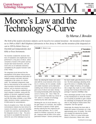
  • 2. quently cofounded Intel along with Robert Noyce, noted that the number of transistors on a silicon chip, plotted as a semi log plot against time, had increased linearly over the preceding 5 years, doubling approxi- mately every 18 months. Moore reasoned that continued improvements in manufactur- ing technology, innovation (device design) and chip size should enable that trend to continue for several more years. Just how well Moore predicted the industry trend can be seen in Figure 1, which shows a semi- log plot of the number of transistors in the various generations of microprocessor chips against time through 2000 indicating con- tinuation of the linear trend for the past 35 years! So accurate was Moore’s prediction, it has become enshrined in the industry lore as Moore’s Law, and subsequently codified as the International Road Map for Semiconductors. For forty years, Moore’s Law has been the yardstick driving innova- tion as semiconductor manufacturers contin- ually strove to gain competitive advantage by being first to market at the next technolo- gy node within the time frame ‘specified’ by Moore’s Law, or even earlier. Indeed, ‘beat Moore’s Law’ has become the com- petitive mantra for leading-edge firms. Moore’s Law is an example of a classic S- curve whereby performance as measured by some convenient metric, e.g., speed, plotted on a linear scale follows the shape of an S over time, ultimately reaching a limit determined by some fundamental phys- ical constraint associated with the underly- ing technology, such as a basic law of physics (Figure 2). At this point, the tech- nology is mature with no potential for fur- ther improvement. To understand how the industry has been able to adhere to the trajectory of Moore’s Law, it will be helpful to have an under- standing of the underlying technologies used to manufacture integrated circuits. Principal among these is optical lithogra- phy, shown schematically in Figure 3. A silicon wafer is first oxidized to create a thin film of silicon dioxide on the surface of the wafer. The wafer is then coated with a thin film of a photosensitive material called a photoresist, and exposed to a patterned source of radiation (by means of a pho- tomask) to form a latent image of the mask pattern in the photoresist. Development of that latent image creates a three-dimension- al replica of the two-dimensional mask pat- tern in the photoresist. The process is analo- gous to photography with the exposure tool equivalent to the camera, and the photore- sist equivalent to the photographic film. Etching the oxide layer bares the silicon substrate, enabling subsequent modification of the electrical properties in these precisely patterned areas. As seen in Figure 3, there are two critical requirements associated with the lithograph- ic process - tools to translate the circuit image into a spatially modulated aerial image, and resist materials to record that image as a latent image, which can subse- quently be developed to form a three- dimensional pattern in the resist film. Both are highly interdependent. Development of a suitable resist requires tailoring the photo- chemistry of the resist to the wavelength associated with the exposure tool, and development of the tool requires availability of a suitable photoresist. Both exposure tool and resist must be commercially available to the chip manufacturer in the timeframe "dictated" by Moore’s Law. The problem is that the development of viable lithographic tools and process tech- nologies takes a considerable period of time - typically10 years and more, which means that technology choices must be made long before the extant technology has matured. Why should this be a prob- lem? In the early 1970s, technologists believed, based on prevailing knowledge of physics and materials science, that diffraction/engi- neering constraints would limit the resolu- tion of optical lithography to around 2.0 micro meters (µm). Hence, practical realiza- tion of Moore’s Law beyond feature sizes of 2.0µm would require development of an alternative exposure technology offering Continued on next page FIGURE 2. Technology S-curve FIGURE 3. Lithographic Fabrication Scheme
  • 3. higher resolution. Although the optical per- formance "limit" was not anticipated for several more years, early choice and devel- opment of a substitute technology was needed in order to assure timely availability of the next generation of manufacturing technology. In response, advanced R&D organizations, such as Bell Labs, IBM, Texas Instruments, Hitachi, and others began around 1970 to pour millions of dol- lars into the development of electron beam lithography, which was seen as the logical successor to optical lithography. Committing to a successor technology and development timeframe long before the extant technology has matured carries enor- mous risk. Factors include: • The correctness of the assessment of the performance limit associated with the prevailing technology • Potential for development of sustain- ing technologies enabling further pro- gression along the technology S-curve, i.e., the predicted performance limit derives from engineering limitations of the prevailing technology, not with the larger optical lithography paradigm • The technical and economic viability of the substitute technology Failure to adequately consider these risks may result in flawed technology strategies and business decisions that can threaten the viability of the business. In the case of optical lithography, the pre- diction of 2.0µm as the performance limit proved completely wrong. Subsequent improvements in sustaining technologies associated with optical lithography, espe- cially the development of reduction step- and-repeat printing tools employing shorter and shorter wavelengths, enabled printing of circuit features well below 2.0µm. However, this was not before millions and millions of dollars had been spent on devel- oping scanning electron beam exposure tools, that subsequently came to be viewed as impractical for chip manufacture, not for reasons of resolution, but of throughput limi- tations, which made manufacturability uneconomical. Fortuitously, the investment in e-beam lithog- raphy was not entirely wasted. Bell Labs recognized that this technique was ideal for making the masks used in photolithography, and subsequently commercialized their elec- tron beam exposure system known as EBES, together with the associated resist technolo- gy also developed at Bell Labs. The EBES system, commercialized by the ETEC corpo- ration as MEBES, has been the industry standard for e-beam mask making since its introduction in the mid 1970s. As the 1980s approached, the industry again faced a critical decision. Recognizing that the diffraction limitations of optical lithography were wavelength dependent (the limit was now thought to be around 1.0um), technologists recognized that diffraction effects could be all but elimi- nated by making a two to three- order of magnitude reduction in wavelength by mov- ing to the X-ray region. Again, millions and millions of dollars were committed to the development of X-ray lithography by Bell Labs, IBM and others. Again, these deci- sions proved to be highly flawed. Continued advances in the technologies sus- taining optical lithography enabled fabrica- tion of devices in the sub-micron regime. Further, as with direct write e-beam lithogra- phy, X-ray lithography also proved to be impractical for commercial implementation because of engineering constraints associat- ed with source and mask. Those constraints proved insurmountable, and those who embraced the X-ray lithography paradigm ended up writing off the hundreds of mil- lions of dollars in investment, and in a num- ber of cases, claiming bankruptcy. It is interesting to speculate whether these mistakes could have been avoided, or at least the investment losses minimized. The quest for an alternative to optical lithogra- phy was driven by inaccurate predictions of the performance limit of the technology. It had been recognized in the 1970s that res- olution, defined by the Rayleigh equation as W = k1λ/2NA where λ is the exposing wavelength, NA the numerical aperture of the lens in the exposure tool, and k a pro- cessing constant, was theoretically much less than 2.0µm. There was no evidence to suggest, however, that the wavelengths and numerical apertures could be realized that would enable such improvements. The incorporation of short wavelength lasers, for example, used in today’s advanced steppers could not have even been con- ceived back in 1970. In other words, the predictions of the demise of optical lithogra- phy were limited by assumptions regarding the prevailing engineering technology not fundamental physical limitations. In reality, the S-curve encompassing Moore’s Law is a composite of multiple S-curves associated with the underlying sustaining technologies, which include • Mask • Light Source - Wavelength, bandwidth • Image Projection • Optics - Materials (Chemistry) - Aberration, Distortion (Physics) • Tools - Engineering • Resists FIGURE 4. Resist Evolution showing material platform transitions required by changes in wavelength of the exposure tools
  • 4. As the history of optical lithography has shown, claiming the demise of a technolo- gy based on the development status of some subset of sustaining technologies can be highly flawed. Improvements in lens technology (materials and engineering) have subsequently enabled fabrication of lenses with close to theoretical numerical apertures. Improvements in laser technolo- gy have enabled practical light sources at wavelengths down to 157nm. Improvements in mask technology have enabled implementation of wavelength engineering techniques and k-factors per- mitting fabrication of devices with minimum feature size less than half the exposing wavelength. Continued improvements in materials technology enabled development of resists matched to the shorter and short- er wavelengths of evolving stepper tools. Over time, the development path of each of these technologies continued to evolve along their individual S-curves (See Figure 4 which illustrates the evolution of resist technology by wavelength with different platforms emerging as the previous platform reached its limit of performance). Convolution of these individual S-curves has enabled continued progression along the composite S-curve for optical lithography. The problem faced by the industry over the years has been in accurately assessing just where the technology in question lies on the S-curve, and the difficulty of the techni- cal challenge limiting the attainment of optimum performance. Had the develop- ments in the technologies supporting opti- cal lithography been foreseen, the millions of dollars in R&D costs invested by the industry in alternative technologies might have been forestalled. Perhaps, but herein lies the tyranny of Moore’s Law and the pressure it creates for the semiconductor industry. Moore’s Law says nothing about the manufacturing tech- nology associated with a given technology node, only the timeframe in which it will be available, i.e., it defines the time frame for technology evolution, without specifying what that technology should or will be. In this context, Moore’s law is simply an expression of faith in the engineering com- munity’s ability to have a manufacturing solution available in the required time- frame. Given the long lead-time for technology development in the semiconductor industry, management must make a rational assess- ment of practical performance "limits" of the prevailing technology and decide whether they reflect a true performance limitation caused by some underlying phys- ical principle, or an engineering limitation in one or more of the sustaining technolo- gies. S-curve methodology tells us that if we are at the physical limit of performance of a prevailing technology, we have no choice but to opt for the discontinuity, pro- vided a viable technology and business model can be implemented. The choice is more difficult when the limita- tions are perceived as engineering in nature. The industry’s commitment to Moore’s Law precludes the luxury of wait- ing to see if developments in the prevailing technology prove capable of meeting man- ufacturing needs several years hence. The risks of adopting such a technology strate- gy are simply too great. Hence the strategy of the industry has been to do both, viz., attempting to solve the engineering prob- lems thereby moving further up the S-curve of the prevailing optical technology, while evaluating alternative approaches aimed at creating technological discontinuity. Had the industry realized back in 1970 just how far it was from the true physical limita- tion of optical lithography, it may not have committed the level of funds that it did to the alternative technologies of e-beam and X-ray. The fact is it did not know, which drove the leading edge companies to hedge their bets by pursuing e-beam and X-ray lithography in addition to efforts aimed at continuing the optical paradigm. The optical lithography example demon- strates another tenet of S-curve thinking, viz., the extant technology will continue to prevail as long as it provides an economic solution to the problems it confronts. The ultimate resolution capability of e-beam lithography is higher than that of optical lithography, but given the continued evolu- tion of optical technology to meet indus- try’s needs over the past 40 years, there has been no economic incentive to switch to e-beam. As a general rule, the invest- ment in the prevailing technology is so great that industry will extract every last measure of performance before switching to an alternative. This tenet also holds true within the technologies sustaining optical lithography. Taking wavelength as an example, the switch by the industry to the next (lower) wavelength has invariably taken place only when the diffraction limit of the preceding wavelength has been reached. This has important implications for resist developers who must anticipate resolution needs encompassed by a partic- ular exposure technology, in order to opti- mize their R&D investment profile. How much further will optical lithography extend? And what lies beyond? As was the case in 1970, massive investments con- tinue to be made in alternative next gener- ation lithographic technogies (NGL) in anticipation of the death of optical lithogra- phy, which is now expected around 50nm. The front-runners are extreme ultraviolet (EUV) and projection e-beam, but both have engineering limitations that remain to be overcome. Today, there is even talk of the death of Moore’s Law itself which, like the Concorde airplane, will likely be driven by economic constraints rather than tech- nology capability. s Murrae Bowden is Executive in Residence and Director of the Executive Master of Technology Management program at the Wesley J. Howe School of Technology Management (mbowden@stevens.edu). Dr. Bowden has had a distin- guished 30-year career in research and research management in the telecommunications and chemical industries, includ- ing the positions of Director, R&D Microelectronics Materials Division, Arch Chemicals (formerly Olin Microelectronic Materials), and Assistant Vice President, Network Technologies Research, Bell Communications Research (Bellcore). About theAuthor