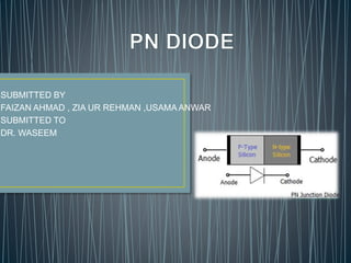
3. • A PN diode is formed by joining P-type material and N-
type material together.
• There are three possibilities:
• No Biased
• Forward Biased
• Reverse Biased
• What is biased?
• Application of external voltage across two terminal.
• Symbol of diode is
4. • Process of moving of majority
charge carrier from Higher to
Lower concentration is known as
diffusion and the current is
called Diffusion current.
• Depletion region is formed after recombination
process, in which immobile ions are surface out.
Holes
5. • No further movement of charges.
• +ve immobile ions repel hole from P-side,
• -ve immobile ions will repel electron from N- side.
• Hence the depletion region act as barrier.
• There is drift current due to minority charge carrier and in
the direction of electric field.
Depletion RegionP N
e
6. • +ve terminal of battery will repels the holes and –ve
terminal repels the electrons towards the depletion
region, because of this depletion region decrease.
• The flood of electron will pass through the junction and
current rises exponentially.
New Depletion Region
Id
Id
Depletion region
7. • +ve terminal of battery will attract the electrons and the –
ve terminal will attract the holes, due to this the depletion
region increase.
• There is only one current due to minority charge carrier,
known as reverse saturation current.
New region
Is Is
- +
8. • Diode current relation is given as:
ID=IS(eVD/nVT -1)
IS=Reverse saturation current.
VD= Biased Voltage.
n= Ideality Factor.
VT=KTK/q
TK= Temperature in Kelvin.
K=1.38*10-23J/K
9. • For No Biased VD=0
• ID=IS(e0- 1)
• ID=IS(1- 1)
• ID=0
• In no biased there is no current through the diode as
shown in diagram.
Ge Si
G eSi
0.3 0.7
10. • For Forward Biased VD increase & Potential Barrier
decrease.
• For Silicon Potential Barrier 0.7 and for Germanium 0.3.
• When VD< Potential Barrier,
• no current flow.
• When VD>= Potential Barrier current will exponentially
rise as shown in fig.
0.3 0.7
siGe
11. • For reversed Biased
• VD<0 so,
ID=IS(eVD/nVT -1)
Become –ve and so
small we can neglect.
• ID=IS(0 -1)
• ID=-IS
• In reverse Biased condition we know that there is only reverse
saturation current due to minority charge carrier as shown in
fig.
S
i
Ge
GeSi
0.3 0.7
12. • When we increase the reverse Biased voltage at higher
value, There is sudden rise in current as show in above
fig.
• This is known as breakdown voltage. At this breakdown
of diode occur.
• What is breakdown?
• When we increase the voltage, electron will acquire very
high Kinetic energy. They will break the covalent bond
and become free. This free electron collide with other
electron and free then the process continue like the
chain.
• Peak inverse voltage:
• Maximum reverse biased voltage that can be applied
across the diode before entering to the break down
region.