This document presents a proposed VLSI architecture for a reversed-trellis tail-biting convolutional code (RT-TBCC) decoder aimed at improving decoding efficiency for LTE applications. The RT-TBCC algorithm is designed to minimize computation while maintaining accuracy, offering a non-iterative approach that contrasts with traditional iterative algorithms. The architecture is evaluated through simulations and FPGA synthesis, demonstrating significant reductions in computational time and resource usage compared to existing solutions.
![International Journal of Electrical and Computer Engineering (IJECE)
Vol. 8, No. 1, February 2018, pp. 198~209
ISSN: 2088-8708, DOI: 10.11591/ijece.v8i1.pp198-209 198
Journal homepage: http://iaescore.com/journals/index.php/IJECE
Reversed-Trellis Tail-Biting Convolutional Code (RT-TBCC)
Decoder Architecture Design for LTE
Trio Adiono, Ahmad Zaky Ramdani, Rachmad Vidya Wicaksana Putra
University Center of Excellence on Microelectronics, Institut Teknologi Bandung, Indonesia
Article Info ABSTRACT
Article history:
Received Mar 8, 2017
Revised Nov 3, 2017
Accepted Nov 17, 2017
Tail-biting convolutional codes (TBCC) have been extensively applied in
communication systems. This method is implemented by replacing the fixed-
tail with tail-biting data. This concept is needed to achieve an effective
decoding computation. Unfortunately, it makes the decoding computation
becomes more complex. Hence, several algorithms have been developed to
overcome this issue in which most of them are implemented iteratively with
uncertain number of iteration. In this paper, we propose a VLSI architecture
to implement our proposed reversed-trellis TBCC (RT-TBCC) algorithm.
This algorithm is designed by modifying direct-terminating maximum-
likelihood (ML) decoding process to achieve better correction rate. The
purpose is to offer an alternative solution for tail-biting convolutional code
decoding process with less number of computation compared to the existing
solution. The proposed architecture has been evaluated for LTE standard and
it significantly reduces the computational time and resources compared to the
existing direct-terminating ML decoder. For evaluations on functionality and
Bit Error Rate (BER) analysis, several simulations, System-on-Chip (SoC)
implementation and synthesis in FPGA are performed.
Keyword:
LTE
Maximum likelihood
Reversed-trellis algorithm
Tail biting convolutional code
VLSI architecture
Copyright © 2018 Institute of Advanced Engineering and Science.
All rights reserved.
Corresponding Author:
Trio Adiono,
University Center of Excellence on Microelectronics,
Institut Teknologi Bandung,
Ganesha Street No. 10, Bandung 40132, Indonesia.
Email: tadiono@stei.itb.ac.id
1. INTRODUCTION
The Viterbi algorithm has a crucial part in a convolutional code (CC) decoding process [1]. It is
highly respected and extensively used because of its high coding gain for convolutional code decoding [2].
Viterbi algorithm is an optimum algorithm that uses the selection of state and data to find the highest
probability of reconstructed data through trellis diagram. Selection is based on total inequality value between
each state line value (i.e. branch metric) and received codewords. Viterbi algorithm works by comparing the
received codewords with prediction data for determining the valid reconstructed bit [3]. Sequence with the
minimum difference to the received codewords is selected as maximum-likelihood (ML) data. It means that
the corresponding sequence is considered as reconstructed data.
Convolutional code has three schemes related to its initial state, namely direct-terminating (unfixed-
tail) CC, fixed-tail CC, and tail-biting CC (TBCC) [4]. The direct-terminating based encoding is unchained
processes. Both of initial and final states are not chained in a circular scheme. It is given a freedom to contain
any data without any correlation. This scheme offers high coding efficiency, although it may result start-up
errors. The predecessor path may meet with the valid path and the rest of bits are eventually decoded
correctly. It is contrarian to the fixed-tail based scheme. Here, the information data are framed by several
additional padding bits before encoding. The additional bits are used as initial state and recognized by the
decoder. The conventional bits used are all zero (i.e. zero padding). It is effective in improving survivor](https://image.slidesharecdn.com/v233nov178mar14932-31882-2-ed-201105055755/85/Reversed-Trellis-Tail-Biting-Convolutional-Code-RT-TBCC-Decoder-Architecture-Design-for-LTE-1-320.jpg)
![International Journal of Electrical and Computer Engineering (IJECE)
Vol. 8, No. 1, February 2018, pp. 198~209
ISSN: 2088-8708, DOI: 10.11591/ijece.v8i1.pp198-209 198
Journal homepage: http://iaescore.com/journals/index.php/IJECE
Reversed-Trellis Tail-Biting Convolutional Code (RT-TBCC)
Decoder Architecture Design for LTE
Trio Adiono, Ahmad Zaky Ramdani, Rachmad Vidya Wicaksana Putra
University Center of Excellence on Microelectronics, Institut Teknologi Bandung, Indonesia
Article Info ABSTRACT
Article history:
Received Mar 8, 2017
Revised Nov 3, 2017
Accepted Nov 17, 2017
Tail-biting convolutional codes (TBCC) have been extensively applied in
communication systems. This method is implemented by replacing the fixed-
tail with tail-biting data. This concept is needed to achieve an effective
decoding computation. Unfortunately, it makes the decoding computation
becomes more complex. Hence, several algorithms have been developed to
overcome this issue in which most of them are implemented iteratively with
uncertain number of iteration. In this paper, we propose a VLSI architecture
to implement our proposed reversed-trellis TBCC (RT-TBCC) algorithm.
This algorithm is designed by modifying direct-terminating maximum-
likelihood (ML) decoding process to achieve better correction rate. The
purpose is to offer an alternative solution for tail-biting convolutional code
decoding process with less number of computation compared to the existing
solution. The proposed architecture has been evaluated for LTE standard and
it significantly reduces the computational time and resources compared to the
existing direct-terminating ML decoder. For evaluations on functionality and
Bit Error Rate (BER) analysis, several simulations, System-on-Chip (SoC)
implementation and synthesis in FPGA are performed.
Keyword:
LTE
Maximum likelihood
Reversed-trellis algorithm
Tail biting convolutional code
VLSI architecture
Copyright © 2018 Institute of Advanced Engineering and Science.
All rights reserved.
Corresponding Author:
Trio Adiono,
University Center of Excellence on Microelectronics,
Institut Teknologi Bandung,
Ganesha Street No. 10, Bandung 40132, Indonesia.
Email: tadiono@stei.itb.ac.id
1. INTRODUCTION
The Viterbi algorithm has a crucial part in a convolutional code (CC) decoding process [1]. It is
highly respected and extensively used because of its high coding gain for convolutional code decoding [2].
Viterbi algorithm is an optimum algorithm that uses the selection of state and data to find the highest
probability of reconstructed data through trellis diagram. Selection is based on total inequality value between
each state line value (i.e. branch metric) and received codewords. Viterbi algorithm works by comparing the
received codewords with prediction data for determining the valid reconstructed bit [3]. Sequence with the
minimum difference to the received codewords is selected as maximum-likelihood (ML) data. It means that
the corresponding sequence is considered as reconstructed data.
Convolutional code has three schemes related to its initial state, namely direct-terminating (unfixed-
tail) CC, fixed-tail CC, and tail-biting CC (TBCC) [4]. The direct-terminating based encoding is unchained
processes. Both of initial and final states are not chained in a circular scheme. It is given a freedom to contain
any data without any correlation. This scheme offers high coding efficiency, although it may result start-up
errors. The predecessor path may meet with the valid path and the rest of bits are eventually decoded
correctly. It is contrarian to the fixed-tail based scheme. Here, the information data are framed by several
additional padding bits before encoding. The additional bits are used as initial state and recognized by the
decoder. The conventional bits used are all zero (i.e. zero padding). It is effective in improving survivor](https://image.slidesharecdn.com/v233nov178mar14932-31882-2-ed-201105055755/75/Reversed-Trellis-Tail-Biting-Convolutional-Code-RT-TBCC-Decoder-Architecture-Design-for-LTE-1-2048.jpg)
![Int J Elec & Comp Eng ISSN: 2088-8708
Reversed-Trellis Tail-Biting Convolutional Code (RT-TBCC) Decoder Architecture …. (Trio Adiono)
199
routes convergence, but inefficient data rate emerges as issue to be dealt with since the non-informative data
is added as initial state [4]. Lastly, in the TBCC, the encoded data must be formed from identical initial and
final state to assure that received code is the valid one [4,5]. This scheme is considered to cover the
advantages of both, direct-terminating (unfixed-tail) and fixed-tail CC because it uses informative data in
initial state that help to decode the information better.
In order to implement TBCC, there are various sub-optimum techniques based on the Viterbi
algorithm such as Circular Viterbi Algorithm (CVA) [6], Warped Around Viterbi Algorithm (WAVA) [7],
Bidirectional Viterbi Algorithm (BVA) [8], improvement of CVA [7] and the combination of Viterbi and A*
Algorithm [9]. As an alternative, we also proposed a technique that suits the hardware implementation named
Reversed-Trellis TBCC (RT-TBCC) algorithm [4]. This algorithm is non-iterative and designed for
minimizing the number of computation, thus a more efficient hardware implementation can be obtained. It
overcomes start-up errors on the direct-terminating CC by separating the processing trellis into two parts,
start-up and common area. It computes the start-up and common area first and collect all of the required data.
Afterwards, the reverse decoding is performed until reaching the initial state. The data with minimum error is
selected as valid data.
Arguably, the non-iterative algorithm is important for hardware implementation because it has a
minimum and predictable number of computation. Thus, the power consumption is efficient and predictable
as well. The iterative one could make the number of computation unpredictable. For example, one data frame
could be decoded for less than x iteration, but there is no guarantee that the upcoming data frame could be
decoded at the same number of iteration since it depends on the result. As long as the result is not tail-biting,
the process keeps running. This may cause higher power consumption to decode the same size of data frame.
The proposed algorithm tries to deal with that problem by minimizing the number of computation while
maintaining the accuracy of tail-biting process. Hopefully, it is a decent alternative algorithm to perform an
efficient tail-biting decoding process.
In this research, we aim to implement the proposed RT-TBCC algorithm in a VLSI architecture. It is
obtained by using three steps on design methodology, namely processing element (PE) design, reversed-
trellis unit (RTU) design and top-level integration. For real-time LTE standard application, plug-and-play
approach is used for integrating the RT-TBCC VLSI module into LEON3-based System-on-Chip (SoC).
This paper is organized in a number of sections. First is introduction of the research background.
Second is related theories. It is followed by explanation on the RT-TBCC algorithm in the third section. A
step-by-step description of the algorithm is also presented. The fourth section is the proposed modular
hardware and System-on-Chip (SoC) implementations for LTE application. Results and discussions are given
in the fifth section. Lastly, conclusions, acknowledgment, and references are given in the three two sections,
respectively.
2. RELATED THEORIES
Convolutional encoding process is usually characterized in (c, n, m), with n/c is code rate (R) and m
is constraint length. There are three kinds of CC based on its initial state, namely direct-terminating (unfixed-
tail) CC, fixed-tail CC, and tail-biting convolutional codes (TBCC). Each of them has a unique approach of
computation regarding its target of design.
The direct-terminating CC is unchained encoding process. Thus, if it is declared as (c, 1, m), then for
each sequence of length L, it generates a codeword with length c × L because no additional data in the
encoding process. In the fixed-tail CC scheme, information data are framed by several additional padding bits
before encoding process. For data length L, it produces a codeword (L+m) × c so that there are losses of data
rate by m / (L+m). Lastly, the TBCC generates codeword of length (L+m) × c, similar with fixed-tail CC, but
the data length is (L+m) instead of L because the initial state is not additional bits but the end-part of the data
itself. A complete illustration of these three schemes can be seen in Figure 1.
Figure 1. Differences between three initial-state scenarios in CC process](https://image.slidesharecdn.com/v233nov178mar14932-31882-2-ed-201105055755/85/Reversed-Trellis-Tail-Biting-Convolutional-Code-RT-TBCC-Decoder-Architecture-Design-for-LTE-2-320.jpg)
![ ISSN: 2088-8708
Int J Elec & Comp Eng, Vol. 8, No. 1, February 2018 : 198 – 209
200
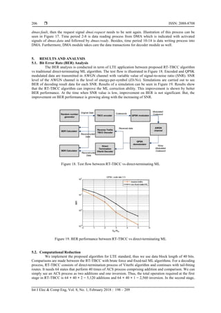
3. REVERSED-TRELLIS TBCC ALGORITHM
The idea of reversed-trellis TBCC (RT-TBCC) algorithm is to find how tail-biting based Viterbi
decoding process can be finished without iteration or at least has a fixed processing time [10]. Since the RT-
TBCC algorithm is established from TBCC concept, it also utilizes the same initial and end states concept.
The difference is that the proposed RT-TBCC exploits the advantages in fixed-tail and direct-terminating
concepts to determine the minimum error trellis path. From three schemes explained before (Figure 1), we
find that the differences between the direct-terminating and fixed-tail based decoding only occur on the trellis
path k < m, with k is trellis order and m is constraint length. Meanwhile, in area k > m, the trellis processes
are common [4]. These are illustrated in Figure 2 and Figure 3. In other words, we can simply state that RT-
TBCC algorithm performing two processes of Viterbi algorithm on two opposite directions. It is similar with
BVA algorithm [8]. The main difference is that the BVA performs bidirectional Viterbi algorithm from the
middle of trellis, meanwhile the RT-TBCC performs bidirectional Viterbi algorithm from m instead of the
middle of trellis. In the RT-TBCC, there are four stages involved based on the operational separation [4].
Figure 2. Fixed-tail CC trellis with „00‟ Figure 3. Direct-terminating CC trellis
The first process is to execute a direct-terminating Viterbi algorithm with an assumption that all
states could be the valid initial state. This process is executed for 0 < k < m (i.e. start-up stage). Illustration is
given in Figure 4 for case-study m = 2. In this process, the received data are stored for next stage
computation. If there is path metric (PMt,k) value for state t at time k, and a branch metric (BMt’,k) value from
state transition t’ → t, with t’ and t” are previous state from t, therefore (1) is applied. From (1), we can
calculate the cost of each path in this first step as (2).
Figure 4. RT-TBCC first stage – start-up Figure 5. RT-TBCC second stage – common
Figure 6. Convergent starting state at “11” and
k = m = 2
Figure 7. All possible tail-biting routes](https://image.slidesharecdn.com/v233nov178mar14932-31882-2-ed-201105055755/85/Reversed-Trellis-Tail-Biting-Convolutional-Code-RT-TBCC-Decoder-Architecture-Design-for-LTE-3-320.jpg)

![Int J Elec & Comp Eng ISSN: 2088-8708
Reversed-Trellis Tail-Biting Convolutional Code (RT-TBCC) Decoder Architecture …. (Trio Adiono)
203
4.3. Path Metric Unit
Path Metric Unit (PMU) is responsible for storing the route matrices which have been passed
through. Records of routing paths and initial states are stored here. Thus, we can easily recall them when
needed. PMU is established from modular Path Metric Cell (PMC) unit. This unit receives two input ports for
state-butterfly pair function and a flag signal. This flag is produced by ACS and passed to PMC for selecting
a prospective path for each state. Internal structure of PMC is shown in Figure 12. Each PMC unit is
connected to each other to mimic butterfly-like pair structure for trellis computation. Number of PMCs
depend on the state used for the computation.
Figure 12. PMC internal structure
4.4. Best State Unit
Best State Unit (BSU) is responsible to compute the total costs and result minimum cost with its
corresponding routing path. It receives total costs information after all processing are finished. There are two
kind of costs which come from common stage and reversed-trellis stage processes. In order to find the
minimum cost, sorting is used. Sorting processes are done for 64 paths from each state. Sorting process is
conducted if the traceback processes are finished. Since the proposed architecture is designed for LTE
standard, the total number of traceback steps are 40.
4.5. Reversed-Trellis Unit
Reverse trellis unit (RTU) work scheme is to calculate the path cost in area k < m, which the paths
have been determined earlier and stored during the process of Viterbi algorithm on the first stage. Illustration
of the complete reversed-trellis block diagram can be seen in Figure 13. There are five modules inside RTU,
namely first sequence buffer, branch metric calculator, route shift register, hamming calculator and tail-biting
cost. Data input are stored in the first sequence buffer until RTU ready to process new data block. If the
Viterbi decoding process is finished, information data from PMU are used as routing reference for cost
calculation. The bit-shift routing and its cost calculation, as illustrated in Figure 8, are done in route shift
register and branch metric calculator. After each bit-shifting process, cost of the route is included to hamming
calculator and combined with the cost generated from stage-two, in order to get the final value. The final
value is calculated in tail-biting cost module and the minimum routing cost is considered as the valid
reconstructed data.
Figure 13. Reversed-trellis block diagram
4.6. Top-Level Architecture
Since the application target is LTE standard, we need 100 Mbps throughput in the system [11], [12].](https://image.slidesharecdn.com/v233nov178mar14932-31882-2-ed-201105055755/85/Reversed-Trellis-Tail-Biting-Convolutional-Code-RT-TBCC-Decoder-Architecture-Design-for-LTE-6-320.jpg)
![Int J Elec & Comp Eng ISSN: 2088-8708
Reversed-Trellis Tail-Biting Convolutional Code (RT-TBCC) Decoder Architecture …. (Trio Adiono)
205
applications. This feature makes SoC has successfully driven many electronic based product developments
[13]. Various devices for diverse applications are basically established from SoC technology [14]. To utilize
the error correction capability in real-time applications, CC decoder is considered to be integrated in such a
hardware-software co-design system [2]. Thus, in the proposed system, the RT-TBCC design is integrated
into SoC as one of its modules. The proposed SoC design for RT-TBCC implementation is presented in
Figure 16. We use LEON3 based SoC as reference design. We attach the RT-TBCC decoder as co-processor
which is located as a slave module in AHB bus of SoC. Moreover, we also incorporate direct memory access
(DMA) module for accelerating data transfer from RT-TBCC decoder, because we need to achieve 100 Mbps
target speed for LTE standard.
Figure 16. RT-TBCC SoC implementation
Figure 17. DMA access timing diagram
For DMA processing, it is started with providing valid data on the signals except dmai.request
signal. After those the signals are valid, dmai.request is activated “high”. It means that the system is
requesting DMA access. If dmao.grant signal responds with “high”, it means that the request has been
granted. Afterwards, the system waits a response from dmao.okay, dmao.retry or dmao.fault signals. If there
is no response yet, the dmai.request continues as “high”. If the one which respond “high” is dmao.okay, then
the system continues to wait the dmao.ready signal. The dmao.ready valid signal means that the
corresponding dmao.data signals are valid. Otherwise, if the one which respond “high” is dmao.retry or](https://image.slidesharecdn.com/v233nov178mar14932-31882-2-ed-201105055755/85/Reversed-Trellis-Tail-Biting-Convolutional-Code-RT-TBCC-Decoder-Architecture-Design-for-LTE-8-320.jpg)
![ ISSN: 2088-8708
Int J Elec & Comp Eng, Vol. 8, No. 1, February 2018 : 198 – 209
208
6. CONCLUSION
In this paper, we propose a VLSI architecture to implement our novel reversed-trellis TBCC (RT-
TBCC) algorithm. It is a non-iterative algorithm developed from direct-terminating ML process with tail-
biting concept. It aims to minimize the number of computation for direct-terminating maximum-likelihood
(ML) decoding process. The RT-TBCC algorithm enables a prediction on the number of computation needed
in the process. The proposed architecture for LTE communication standard demonstrates promising results in
hardware implementation and performance. It requires only 5,712 addition and 3,008 inversion. It is a
significant decrease compared to 286,592 addition and 143,296 inversion for fixed-tail ML decoder and
45,079,976,738,816 addition and 1,099,511,627,776 inversion for brute force algorithm. Moreover, its SoC
implementation can perform computation with 100 Mbps throughput as expected for LTE.
ACKNOWLEGEMENTS
This article is extended version of papers entitled “A novel algorithm of tail biting convolutional
code decoder for low cost hardware implementation” and “Tail biting convolutional code decoder co-
processor for high throughput System-on-Chip” that were published at ISPACS 2015 [4] and ISOCC 2015
[10] respectively.
REFERENCES
[1] A. J. Viterbi, “Error Bounds for Convolutional Coding and an Asymptotically Optimum Decoding Algorithm”,
IEEE Transactions on Information Theory (TIT), vol. 13, no. 2, pp. 260-269, April 1967.
[2] R. V. W. Putra and T. Adiono, “VLSI Architecture for Configurable and Low-Complexity Design of Hard-
Decision Viterbi Decoding Algorithm”, Journal of ICT Research and Applications (JICTRA), vol. 10, no. 1,
pp. 57-75, March 2016.
[3] R. V. W. Putra and T. Adiono, “A Configurable and Low Complexity Hard-Decision Viterbi Decoder in
VLSI Architecture”, Proc. of 2014 2nd International Conference on Information and Communication
Technology (ICoICT), pp. 177-181, May 2014.
[4] A. Z. Ramdani and T. Adiono, “A Novel Algorithm of Tail Biting Convolutional Code Decoder for Low Cost
Hardware Implementation”, Proc. of 2015 International Symposium on Intelligent Signal Processing and
Communication Systems (ISPACS), pp. 241-245, November 2015.
[5] H. H. Ma and J. K. Wolf, “On Tail Biting Convolutional Codes”, IEEE Transactions on Communications (TCOM),
vol. 34, no. 2, pp. 104-111, February 1986.
[6] R. V. Cox and C. E. Sundberg, “An Efficient Adaptive Circular Viterbi Algorithm for Decoding Generalized
Tailbiting Convolutional Codes”, IEEE Transactions on Vehicular Technology, vol. 43, pp. 57-68, February 1994.
[7] R. Shao, S. Lin, and M. Fossorier, “Two Decoding Algorithms for Tailbiting Codes”, IEEE Transactions on
Commununications (TCOMM), vol. 51, no. 10, pp. 1658-1665, October 2003.
[8] X. Wang, H. Qian, J. Xu, Y. Yang, and F. Wang, “An Efficient CVA-based Decoding Algorithm for Tail-Biting
Codes”, Proc. of IEEE Global Telecommunications Conference (GLOBECOM), pp. 1-5, December 2011.
[9] P. Shankar, P. N. A. Kumar, K. Sasidharan, B. S. Rajan, and A. S. Madhu, “Efficient Convergent Maximum
Likelihood Decoding on Tailbiting Trellises”, CoRR, vol. abs/cs/0601023, 2006. URL: http://arxiv.org/
abs/cs/0601023v2
[10] A. Z. Ramdani and T. Adiono, ”Tail Biting Convolutional Code Decoder Co-Processor for High Throughput
System-on-Chip,” Proc. of 2015 International SoC Design Conference (ISOCC), pp. 303-304, November 2015.
[11] A. Z. Yonis and M. F. L. Abdullah, ”Uplink and Downlink of LTE-Release 10 in Celular Communications,” Int. J.
of Informatics and Communication Technology (IJ-ICT), vol. 1, no. 1, pp. 43-53, July 2012.
[12] A. Z. Yonis and M. F. L. Abdullah, ”Peak-Throughput of LTE-Release 10 for Up/Down Link Physical Layer,” Int.
J. of Information and Network Security (IJINS), vol. 1, no. 2, pp. 88-96, June 2012.
[13] R. V. W. Putra and T. Adiono, “Hybrid Multi–System-on-Chip Architecture: A Rapid Development Design for
High-Flexibility System”, Proc. of 2016 International Conference on Electronics, Information, and Communication
(ICEIC), pp. 1-4, January 2016.
[14] R. V. W. Putra and T. Adiono, “Hybrid Multi–System-on-Chip Architecture as Rapid Development Approach for
High-Flexibility System”, IEIE Transactions on Smart Processing and Computing (IEIE-SPC), vol. 5, no. 1, pp.
55-62, February 2016.](https://image.slidesharecdn.com/v233nov178mar14932-31882-2-ed-201105055755/85/Reversed-Trellis-Tail-Biting-Convolutional-Code-RT-TBCC-Decoder-Architecture-Design-for-LTE-11-320.jpg)