SlideShare a Scribd company logo
1 of 11
Microprocessors and programming Chapter2 Mrs. Radhika Kamath, VPMP,Thane 1
Internal Architecture of 8086
• 8086 has two blocks BIU (Bus Interface Unit) and EU (Execution Unit)
• The BIU performs all bus operations such as instruction fetching, reading and writing
operands for memory and calculating the addresses of the memory operands. The
instruction bytes are transferred to the instruction queue.
• EU executes instructions from the instruction system byte queue.
• Both units operate asynchronously to give the 8086 an overlapping instruction fetch
and execution mechanism which is called as Pipelining. This results in efficient use of
the system bus and system performance.
• BIU contains Instruction queue, Segment registers, Instruction pointer, and Address
adder.
• EU contains Control circuitry, Instruction decoder, ALU, Pointer and Index register,
Flag register.
BUS INTERFACR UNIT:
• It provides a full 16 bit bidirectional data bus and 20 bit address bus.
• The bus interface unit is responsible for performing all external bus operations.
It has the following functions:
• Instruction fetch, Instruction queuing, Operand fetch and storage, Address relocation
and Bus control.
• The BIU uses a mechanism known as an instruction stream queue to implement a
pipeline architecture.
• The BIU also contains a dedicated adder which is used to generate the 20bit physical
address that is output on the address bus. This address is formed by adding an
appended 16 bit segment address and a 16 bit offset address.
• The BIU is also responsible for generating bus control signals such as those for
memory read or write and I/O read or write.
Concept of Pipelining with an example:--
Microprocessors and programming Chapter2 Mrs. Radhika Kamath, VPMP,Thane 2
• The BIU uses a mechanism known as an instruction stream queue to implement a
pipeline architecture.
o This queue permits prefetch of up to six bytes of instruction code. When ever
the queue of the BIU is not requesting it to read or write operands from
memory, the BIU is free to look ahead in the program by prefetching the next
sequential instruction.
o These prefetching instructions are held in its FIFO queue. With its 16 bit data
bus, the BIU fetches two instruction bytes in a single memory cycle.
o The EU accesses the queue from the output end. It reads one instruction byte
after the other from the output of the queue.
Concept of pipelining can be explained with the help of an example, where three
instructions need to executed by the processor.
On a non-pipelined processor, nine clock cycles are required for the individual fetch,
decode and execute cycles for three instructions as shown below.
Diagram given in class
On a pipelined processor, where fetch, decode and execute operations are done in
parallel, only five cycles are required as shown below.
Diagram given in class
Thus there is a tremendous performance gain in pipelined processors.
Memory Segmentation :--
o The memory in an 8086 microprocessor is organized as a segmented memory.The
physical memory is divided into 4 segments namely, Data Segment, Code segment, Stack
segment and extra segment. Data segment is used to hold data, Code segment for the
executable program, Extra segment also holds data specifically in strings and stack
segment is used to store stack data. Each segment is 64Kbytes & addressed by one
segment register. The segment registers for four segments are DS register, CS register, ES
register & SS register. The 16 bit segment register holds the starting address of the
segment. Since the memory size of 8086 is 1Mbytes, total 16 segments are possible with
each having 64Kbytes
o The physical address of the memory can range from 00000 to FFFFFH. The offset
address to the segment address is specified as a 16-bit displacement between 0000 to
FFFFH.. The following fig shows the memory segmentation, the base address is the
starting address of the segment
(Diagram given in class)
Advantages of segmentation :--
o Though 8086 has 20 bit address, only 16 bits are sufficient to locate a
memory location
o Programs and data can be stored separately
o By using more than one data or code segements, a large program can eb
executed.
o Useful in multi user time-shared system
o Programs are position independent and re-locatable
o Data can be shared by two processes
o Addressability of a processor can be extended.
Microprocessors and programming Chapter2 Mrs. Radhika Kamath, VPMP,Thane 3
o . The 16 bit offset or displacement is added to the 16 bit segment base register after the
shifting the contents towards left by one digit to get 20 bits physical address.
Physical memory address generation :--
• The 8086 memory has 220
addressable locations, with the help of 16 bits address, though
it has a 20 bit address bus.
• This is possible in the BIU which contains a dedicated adder used to generate the 20bit
physical address which is theoutput on the address bus. This address is formed by adding
an appended 16 bit segment address and a 16 bit offset address. This is generally shown
as given below.
Physical address generation for code segment :--
• CS register is used to hold the 16bit base address of Code segment.
• The IP register is used to hold the 16 bit address of the next byte within the code segment.
This is the offset or the displacement for CS register.
• The physical address of the next instruction to be fetched is formed by combining the
current contents of the code segment CS register and the current contents of the
instruction pointer IP register.
• For e.g., If CS = 3000H, and IP = 1234H, the physical address can be generated as given
below
Steps for the address generation:
Microprocessors and programming Chapter2 Mrs. Radhika Kamath, VPMP,Thane 4
 The 20 bit physical address can be represented as CS:IP for code segment.
 CS is shifted to left by 4 bit positions (1 digit position) as 30000H, which is the base
address for CS segment
 Add IP i.e., 1234H to this base address to obtain 31234H, which is the 20 bit physical
address.
Physical address generation for code segment :--
• SS register is used to hold the 16bit base address of Stack segment.
• The SP register is used to hold the 16 bit starting address of the segment where the word
was most recently stored on the stack. This is called the Top of the stack.
• The physical address of the stack while reading or writing is formed by combining the
current contents of the stack segment SS register and the current contents of the stack
pointerSP register.
• For e.g., If SS = 5000H, and SP = 58F4H, the physical address can be generated as given
below
Steps for the address generation :
 The 20 bit physical address can be represented as SS:SP for stack segment.
 SS is shifted to left by 4 bit positions (1 digit position) as 50000H, which is the base
address for SS segment
 Add SP i.e., 58F4H to this base address to obtain 55F84H, which is the 20 bit physical
address.
EXECUTION UNIT
• The Execution unit is responsible for decoding and executing all instructions.
• The EU extracts instructions from the top of the queue in the BIU, decodes them,
generates operands if necessary, passes them to the BIU and requests it to perform the
read or write bys cycles to memory or I/O and perform the operation specified by the
instruction on the operands.
• During the execution of the instruction, the EU tests the status and control flags and
updates them based on the results of executing the instruction.
• If the queue is empty, the EU waits for the next instruction byte to be fetched and shifted
to top of the queue.
• When the EU executes a branch or jump instruction, it transfers control to a location
corresponding to another set of sequential instructions.
• Whenever this happens, the BIU automatically resets the queue and then begins to fetch
instructions from this new location to refill the queue.
• EU has a 16 bit ALU, which can perform arithmetic and logical operations on 8 bit as
well as 16 bit data.
• Flagregister is a 16-bit register containing 9 one bit flags.
1. Overflow Flag (OF) - set if the result is too large positive number, or is too small
negative number to fit into destination operand.
2. Direction Flag (DF) - if set then string manipulation instructions will auto-
decrement index registers. If cleared then the index registers will be auto-
incremented.
3. Interrupt-enable Flag (IF) - setting this bit enables maskable interrupts.
4. Single-step Flag (TF) - if set then single-step interrupt will occur after the next
instruction.
Microprocessors and programming Chapter2 Mrs. Radhika Kamath, VPMP,Thane 5
5. Sign Flag (SF) - set if the most significant bit of the result is set.
6. Zero Flag (ZF) - set if the result is zero.
7. Auxiliary carry Flag (AF) - set if there was a carry from or borrow to bits 0-3 in
the AL register.
8. Parity Flag (PF) - set if parity (the number of "1" bits) in the low-order byte of
the result is even.
9. Carry Flag (CF) - set if there was a carry from or borrow to the most significant
bit during last result calculation.
Internal Registers of 8086
• The 8086 has four groups of the user accessible internal registers. They are the instruction
pointer (IP), four data registers, four pointer and index register, four segment registers.
• The 8086 has a total of fourteen 16-bit registers including a 16 bit register called the flag
register, with 9 of bits implemented for status and control flags.
• Most of the registers contain data/instruction offsets within 64 KB memory segment.
There are four different 64 KB segments for instructions, stack, data and extra data. To
specify where in 1 MB of processor memory these 4 segments are located the processor
uses four segment registers:
• Code segment (CS) is a 16-bit register containing address of 64 KB segment with
processor instructions. The processor uses CS segment for all accesses to instructions
referenced by instruction pointer (IP) register. CS register cannot be changed directly.
The CS register is automatically updated during far jump, far call and far return
instructions.
• Stack segment (SS) is a 16-bit register containing address of 64KB segment with
program stack. By default, the processor assumes that all data referenced by the stack
pointer (SP) and base pointer (BP) registers is located in the stack segment. SS register
can be changed directly using POP instruction.
• Data segment (DS) is a 16-bit register containing address of 64KB segment with
program data. By default, the processor assumes that all data referenced by general
registers (AX, BX, CX, DX) and index register (SI, DI) is located in the data segment. DS
register can be changed directly using POP and LDS instructions.
• Accumulator register consists of two 8-bit registers AL and AH, which can be combined
together and used as a 16-bit register AX. AL in this case contains the low-order byte of
the word, and AH contains the high-order byte. Accumulator can be used for I/O
operations and string manipulation.
• Base register consists of two 8-bit registers BL and BH, which can be combined together
and used as a 16-bit register BX. BL in this case contains the low-order byte of the word,
and BH contains the high-order byte. BX register usually contains a data pointer used for
based, based indexed or register indirect addressing.
• Count register consists of two 8-bit registers CL and CH, which can be combined
together and used as a 16-bit register CX. When combined, CL register contains the low-
order byte of the word, and CH contains the high-order byte. Count register can be used
in Loop, shift/rotate instructions and as a counter in string manipulation,.
• Data register consists of two 8-bit registers DL and DH, which can be combined together
and used as a 16-bit register DX. When combined, DL register contains the low-order
byte of the word, and DH contains the high-order byte. Data register can be used as a port
number in I/O operations. In integer 32-bit multiply and divide instruction the DX register
contains high-order word of the initial or resulting number.
The following registers are pointer and index registers:
Microprocessors and programming Chapter2 Mrs. Radhika Kamath, VPMP,Thane 6
• Stack Pointer (SP) is a 16-bit register pointing to program stack.
• Base Pointer (BP) is a 16-bit register pointing to data in stack segment. BP register is
usually used for based, based indexed or register indirect addressing.
• Source Index (SI) is a 16-bit register. SI is used for indexed, based indexed and register
indirect addressing, as well as a source data address in string manipulation instructions.
• Destination Index (DI) is a 16-bit register. DI is used for indexed, based indexed and
register indirect addressing, as well as a destination data address in string manipulation
instructions.
8086 Modes of operation :--
8284 clock generator :-- refer class notes
IC245 Bidirectional Buffer
• Also called as Octal bus Transceiver
• Bidirectional bus increases the current driving
capacity of data bus
• Each buffer can sink 24mA and source 15mA.
• Consists of 16 non inverting buffers, eight for each
direction with tri-state outputs.
• G is the enable pin, when G=0,DIR is chosen.
• Direction of data pin decided by DIR pin
• When DIR = 1, Data A bus  B bus
• When DIR =0, Data B bus  A bus
IC373 Octal latch
• Used for the separation of valid addresses from
address/data bus
• Controlled by the ALE signal of microprocessor
• Latch is controlled by E input (STB input)
which is connected to the clock input of D f/f.
• Buffer is controlled by OE pin
General Bus Operation:
• The 8086 has a combined address and data bus
commonly referred as a time multiplexed address
and data bus.
• The main reason behind multiplexing address and data over the same pins is the
maximum utilisation of processor pins and it facilitates the use of 40 pin standard DIP
package.
• The bus can be demultiplexed using a few latches and transreceivers, when ever required.
• Basically, all the processor bus cycles consist of at least four clock cycles. These are
referred to as T1, T2, T3, T4. The address is transmitted by the processor during T1. It is
present on the bus only for one cycle.
Microprocessors and programming Chapter2 Mrs. Radhika Kamath, VPMP,Thane 7
• The negative edge of this ALE pulse is used to separate the address and the data or status
information. In maximum mode, the status lines S0, S1 and S2 are used to indicate the
type of operation.
• Status bits S3 to S7 are multiplexed with higher order address bits and the BHE signal.
Address is valid during T1 while status bits S3 to S7 are valid during T2 through T4.
Minimum Mode 8086 System
• In a minimum mode 8086 system, the microprocessor 8086 is operated in minimum mode
by strapping its MN/MX pin to logic 1.
• In this mode, all the control signals are given out by the microprocessor chip itself. There
is a single microprocessor in the minimum mode system.
• The remaining components in the system are latches, transreceivers, clock generator,
memory and I/O devices. Some type of chip selection logic may be required for selecting
memory or I/O devices, depending upon the address map of the system.
• Latches are generally buffered output D-type flip-flops like 74LS373 or 8282. They are
used for separating the valid address from the multiplexed address/data signals and are
controlled by the ALE signal generated by 8086.
• Transceivers are the bidirectional buffers and some times they are called as data
amplifiers. They are required to separate the valid data from the time multiplexed
address/data signals.
• They are controlled by two signals namely, DEN and DT/R.
• The DEN signal indicates the direction of data, i.e. from or to the processor. The system
contains memory for the monitor and users program storage.
Microprocessors and programming Chapter2 Mrs. Radhika Kamath, VPMP,Thane 8
• The working of the minimum mode configuration system can be better described in terms
of the timing diagrams rather than qualitatively describing the operations.
• The opcode fetch and read cycles are similar. Hence the timing diagram can be
categorized in two parts, the first is the timing diagram for read cycle and the second is
the timing diagram for write cycle.
Minimum Mode Read bus cycle
• The read cycle begins in T1 with the assertion of address latch enable (ALE) signal and
also M / IO signal. During the negative going edge of this signal, the valid address is
latched on the local bus.
• The BHE and A0 signals address low, high or both bytes. From T1 to T4 , the M/IO
signal indicates a memory or I/O operation.
• At T2, the address is removed from the local bus and is sent to the output. The bus is then
tristated. The read (RD) control signal is also activated in T2.
• The read (RD) signal causes the address device to enable its data bus drivers. After RD
goes low, the valid data is available on the data bus.
• The addressed device will drive the READY line high. When the processor returns the
read signal to high level, the addressed device will again tristate its bus drivers.
Microprocessors and programming Chapter2 Mrs. Radhika Kamath, VPMP,Thane 9
Minimum Mode Write bus cycle
• A write cycle also begins with the assertion of ALE and the emission of the address. The
M/IO signal is again asserted to indicate a memory or I/O operation. In T2, after sending
the address in T1, the processor sends the data to be written to the addressed location.
• The data remains on the bus until middle of T4 state. The WR becomes active at the
beginning of T2 (unlike RD is somewhat delayed in T2 to provide time for floating).
• The BHE and A0 signals are used to select the proper byte or bytes of memory or I/O
word to be read or write.
• The M/IO, RD and WR signals indicate the type of data transfer as specified in table
below.
Maximum Mode 8086 System
Microprocessors and programming Chapter2 Mrs. Radhika Kamath, VPMP,Thane 10
• In a maximum mode 8086 system, the microprocessor 8086 is operated in maximum
mode bystrapping the MN/MX pin to ground.
• In this mode, the processor derives the status signal S2, S1, S0. Another chip called bus
controller derives the control signal using this status information.
• In the maximum mode, there may be more than one microprocessor in the system
configuration.
• The components in the system are same as in the minimum mode system.
• The basic function of the bus controller chip IC8288, is to derive control signals like RD
and WR ( for memory and I/O devices), DEN, DT/R, ALE etc. using the information by
the processor on the status lines.
• The bus controller chip has input lines S2, S1, S0 and CLK. These inputs to 8288 are
driven by CPU.
• It derives the outputs ALE, DEN, DT/R, MRDC, MWTC, AMWC, IORC, IOWC and
AIOWC. The AEN, IOB and CEN pins are specially useful for multiprocessor systems.
• AEN and IOB are generally grounded. CEN pin is usually tied to +5V. The significance
of the MCE/PDEN output depends upon the status of the IOB pin.
• If IOB is grounded, it acts as master cascade enable to control cascade 8259A, else it acts
as peripheral data enable used in the multiple bus configurations.
• INTA pin used to issue two interrupt acknowledge pulses to the interrupt controller or to
an interrupting device.
• IORC, IOWC are I/O read command and I/O write command signals respectively. These
signals enable an IO interface to read or write the data from or to the address port.
• The MRDC, MWTC are memory read command and memory write command signals
respectively and may be used as memory read or write signals.
• All these command signals instructs the memory to accept or send data from or to the bus.
• For both of these write command signals, the advanced signals namely AIOWC and
AMWTC are available.
Microprocessors and programming Chapter2 Mrs. Radhika Kamath, VPMP,Thane 11
Maximum mode Read bus cycle operation
• Here the only difference between in timing diagram between minimum mode and
maximum mode is the status signals used and the available control and advanced
command signals.
• R0, S1, S2 are set at the beginning of bus cycle.8288 bus controller will output a pulse as
on the ALE and apply a required signal to its DT / R pin during T1.
• In T2, 8288 will set DEN=1 thus enabling transceivers, and for an input it will activate
MRDC or IORC. These signals are activated until T4. For an output, the AMWC or
AIOWC is activated from T2 to T4 and MWTC or IOWC is activated from T3 to T4.
• The status bit S0 to S2 remains active until T3 and become passive during T3 and T4.
• If reader input is not activated before T3, wait state will be inserted between T3 and T4.
Maximum mode Write Bus cycle

More Related Content

What's hot

Internal architecture-of-8086
Internal architecture-of-8086Internal architecture-of-8086
Internal architecture-of-8086Estiak Khan
 
1326 Introduction To 8086 Microprocessor
1326 Introduction To 8086 Microprocessor1326 Introduction To 8086 Microprocessor
1326 Introduction To 8086 Microprocessortechbed
 
26677766 8086-microprocessor-architecture
26677766 8086-microprocessor-architecture26677766 8086-microprocessor-architecture
26677766 8086-microprocessor-architectureSaurabh Jain
 
Intel 8086 microprocessor
Intel 8086 microprocessorIntel 8086 microprocessor
Intel 8086 microprocessorRavi Yasas
 
Architecture of 8086 microprocessor
Architecture of  8086 microprocessorArchitecture of  8086 microprocessor
Architecture of 8086 microprocessorAnirban Saha Anik
 
8086 Microprocessor
8086 Microprocessor 8086 Microprocessor
8086 Microprocessor Vijay Kumar
 
8086 class notes-Y.N.M
8086 class notes-Y.N.M8086 class notes-Y.N.M
8086 class notes-Y.N.MDr.YNM
 
8086 architecture and pin description
8086 architecture and pin description 8086 architecture and pin description
8086 architecture and pin description Aswini Dharmaraj
 
8086 microprocessor-architecture
8086 microprocessor-architecture8086 microprocessor-architecture
8086 microprocessor-architectureprasadpawaskar
 
8086 Microprocessor powerpoint
8086  Microprocessor  powerpoint8086  Microprocessor  powerpoint
8086 Microprocessor powerpointRandhir Kumar
 
Memory Segmentation of 8086
Memory Segmentation of 8086Memory Segmentation of 8086
Memory Segmentation of 8086Nikhil Kumar
 

What's hot (19)

Cs14 406 mod1
Cs14 406 mod1Cs14 406 mod1
Cs14 406 mod1
 
intel 8086 introduction
intel 8086 introductionintel 8086 introduction
intel 8086 introduction
 
8086 architecture By Er. Swapnil Kaware
8086 architecture By Er. Swapnil Kaware8086 architecture By Er. Swapnil Kaware
8086 architecture By Er. Swapnil Kaware
 
8086
8086 8086
8086
 
Internal architecture-of-8086
Internal architecture-of-8086Internal architecture-of-8086
Internal architecture-of-8086
 
1326 Introduction To 8086 Microprocessor
1326 Introduction To 8086 Microprocessor1326 Introduction To 8086 Microprocessor
1326 Introduction To 8086 Microprocessor
 
26677766 8086-microprocessor-architecture
26677766 8086-microprocessor-architecture26677766 8086-microprocessor-architecture
26677766 8086-microprocessor-architecture
 
8086 MICROPROCESSOR
8086 MICROPROCESSOR8086 MICROPROCESSOR
8086 MICROPROCESSOR
 
Intel 8086 microprocessor
Intel 8086 microprocessorIntel 8086 microprocessor
Intel 8086 microprocessor
 
8086 Architecture
8086 Architecture8086 Architecture
8086 Architecture
 
Architecture of 8086 microprocessor
Architecture of  8086 microprocessorArchitecture of  8086 microprocessor
Architecture of 8086 microprocessor
 
8086 Microprocessor
8086 Microprocessor 8086 Microprocessor
8086 Microprocessor
 
8086 class notes-Y.N.M
8086 class notes-Y.N.M8086 class notes-Y.N.M
8086 class notes-Y.N.M
 
8086 architecture and pin description
8086 architecture and pin description 8086 architecture and pin description
8086 architecture and pin description
 
8086 microprocessor-architecture
8086 microprocessor-architecture8086 microprocessor-architecture
8086 microprocessor-architecture
 
8086 conti
8086 conti8086 conti
8086 conti
 
8086 Microprocessor powerpoint
8086  Microprocessor  powerpoint8086  Microprocessor  powerpoint
8086 Microprocessor powerpoint
 
8086 architecture
8086 architecture8086 architecture
8086 architecture
 
Memory Segmentation of 8086
Memory Segmentation of 8086Memory Segmentation of 8086
Memory Segmentation of 8086
 

Similar to 8086 archi notes final

8086 microprocessor-architecture-120207111857-phpapp01
8086 microprocessor-architecture-120207111857-phpapp018086 microprocessor-architecture-120207111857-phpapp01
8086 microprocessor-architecture-120207111857-phpapp01jemimajerome
 
8086-microprocessor-architecture.ppt
8086-microprocessor-architecture.ppt8086-microprocessor-architecture.ppt
8086-microprocessor-architecture.pptMadhan7771
 
3 organization of intel 8086
3 organization of intel 80863 organization of intel 8086
3 organization of intel 8086ELIMENG
 
The Intel 8086 microprocessor
The Intel 8086 microprocessorThe Intel 8086 microprocessor
The Intel 8086 microprocessorGeorge Thomas
 
8086 microprocessor-architecture-120207111857-phpapp01
8086 microprocessor-architecture-120207111857-phpapp018086 microprocessor-architecture-120207111857-phpapp01
8086 microprocessor-architecture-120207111857-phpapp01destaw belay
 
8086 microprocessor-architecture-120207111857-phpapp01
8086 microprocessor-architecture-120207111857-phpapp018086 microprocessor-architecture-120207111857-phpapp01
8086 microprocessor-architecture-120207111857-phpapp01Siva Raman
 
Presentation on 8086 microprocessor
Presentation on 8086 microprocessorPresentation on 8086 microprocessor
Presentation on 8086 microprocessorDiponkor Bala
 
8086 Architecture ppt.pdf
8086 Architecture ppt.pdf8086 Architecture ppt.pdf
8086 Architecture ppt.pdfUmamaheswariV4
 
8086microprocessor 130821100244-phpapp02
8086microprocessor 130821100244-phpapp028086microprocessor 130821100244-phpapp02
8086microprocessor 130821100244-phpapp02raone1989
 
8086microprocessor 130821100244-phpapp02
8086microprocessor 130821100244-phpapp028086microprocessor 130821100244-phpapp02
8086microprocessor 130821100244-phpapp02Murad Mondol
 
8086microprocessor 130821100244-phpapp02
8086microprocessor 130821100244-phpapp028086microprocessor 130821100244-phpapp02
8086microprocessor 130821100244-phpapp02raone1989
 
8086microprocessor 130821100244-phpapp02
8086microprocessor 130821100244-phpapp028086microprocessor 130821100244-phpapp02
8086microprocessor 130821100244-phpapp02raone1989
 
microprocessor_part_3_compressed_1588259301.pdf
microprocessor_part_3_compressed_1588259301.pdfmicroprocessor_part_3_compressed_1588259301.pdf
microprocessor_part_3_compressed_1588259301.pdfssuserd21262
 

Similar to 8086 archi notes final (20)

8086 microprocessor-architecture-120207111857-phpapp01
8086 microprocessor-architecture-120207111857-phpapp018086 microprocessor-architecture-120207111857-phpapp01
8086 microprocessor-architecture-120207111857-phpapp01
 
Amp
AmpAmp
Amp
 
8086-microprocessor-architecture.ppt
8086-microprocessor-architecture.ppt8086-microprocessor-architecture.ppt
8086-microprocessor-architecture.ppt
 
3 organization of intel 8086
3 organization of intel 80863 organization of intel 8086
3 organization of intel 8086
 
The Intel 8086 microprocessor
The Intel 8086 microprocessorThe Intel 8086 microprocessor
The Intel 8086 microprocessor
 
8086 microprocessor-architecture-120207111857-phpapp01
8086 microprocessor-architecture-120207111857-phpapp018086 microprocessor-architecture-120207111857-phpapp01
8086 microprocessor-architecture-120207111857-phpapp01
 
8086 microprocessor-architecture-120207111857-phpapp01
8086 microprocessor-architecture-120207111857-phpapp018086 microprocessor-architecture-120207111857-phpapp01
8086 microprocessor-architecture-120207111857-phpapp01
 
Presentation on 8086 microprocessor
Presentation on 8086 microprocessorPresentation on 8086 microprocessor
Presentation on 8086 microprocessor
 
Advanced micro -processor
Advanced micro -processorAdvanced micro -processor
Advanced micro -processor
 
8086 microprocessor
8086 microprocessor8086 microprocessor
8086 microprocessor
 
Chapter 2
Chapter 2Chapter 2
Chapter 2
 
8086 Architecture ppt.pdf
8086 Architecture ppt.pdf8086 Architecture ppt.pdf
8086 Architecture ppt.pdf
 
8086microprocessor 130821100244-phpapp02
8086microprocessor 130821100244-phpapp028086microprocessor 130821100244-phpapp02
8086microprocessor 130821100244-phpapp02
 
8086 micro processor
8086 micro processor8086 micro processor
8086 micro processor
 
8086microprocessor 130821100244-phpapp02
8086microprocessor 130821100244-phpapp028086microprocessor 130821100244-phpapp02
8086microprocessor 130821100244-phpapp02
 
8086microprocessor 130821100244-phpapp02
8086microprocessor 130821100244-phpapp028086microprocessor 130821100244-phpapp02
8086microprocessor 130821100244-phpapp02
 
8086microprocessor 130821100244-phpapp02
8086microprocessor 130821100244-phpapp028086microprocessor 130821100244-phpapp02
8086microprocessor 130821100244-phpapp02
 
The 8086 microprocessor
The  8086 microprocessorThe  8086 microprocessor
The 8086 microprocessor
 
8086 architecture
8086 architecture8086 architecture
8086 architecture
 
microprocessor_part_3_compressed_1588259301.pdf
microprocessor_part_3_compressed_1588259301.pdfmicroprocessor_part_3_compressed_1588259301.pdf
microprocessor_part_3_compressed_1588259301.pdf
 

More from HarshitParkar6677 (20)

Wi fi hacking
Wi fi hackingWi fi hacking
Wi fi hacking
 
D dos attack
D dos attackD dos attack
D dos attack
 
Notes chapter 6
Notes chapter  6Notes chapter  6
Notes chapter 6
 
Interface notes
Interface notesInterface notes
Interface notes
 
Chapter6 2
Chapter6 2Chapter6 2
Chapter6 2
 
Chapter6
Chapter6Chapter6
Chapter6
 
8086 cpu 1
8086 cpu 18086 cpu 1
8086 cpu 1
 
Chapter 6 notes
Chapter 6 notesChapter 6 notes
Chapter 6 notes
 
Chapter 5 notes
Chapter 5 notesChapter 5 notes
Chapter 5 notes
 
Chap6 procedures & macros
Chap6 procedures & macrosChap6 procedures & macros
Chap6 procedures & macros
 
Chapter 5 notes new
Chapter 5 notes newChapter 5 notes new
Chapter 5 notes new
 
Notes arithmetic instructions
Notes arithmetic instructionsNotes arithmetic instructions
Notes arithmetic instructions
 
Notes all instructions
Notes all instructionsNotes all instructions
Notes all instructions
 
Notes aaa aa
Notes aaa aaNotes aaa aa
Notes aaa aa
 
Notes 8086 instruction format
Notes 8086 instruction formatNotes 8086 instruction format
Notes 8086 instruction format
 
Misc
MiscMisc
Misc
 
Copy of 8086inst logical
Copy of 8086inst logicalCopy of 8086inst logical
Copy of 8086inst logical
 
Copy of 8086inst logical
Copy of 8086inst logicalCopy of 8086inst logical
Copy of 8086inst logical
 
Chapter3 program flow control instructions
Chapter3 program flow control instructionsChapter3 program flow control instructions
Chapter3 program flow control instructions
 
Chapter3 8086inst stringsl
Chapter3 8086inst stringslChapter3 8086inst stringsl
Chapter3 8086inst stringsl
 

Recently uploaded

main PPT.pptx of girls hostel security using rfid
main PPT.pptx of girls hostel security using rfidmain PPT.pptx of girls hostel security using rfid
main PPT.pptx of girls hostel security using rfidNikhilNagaraju
 
Call Girls Narol 7397865700 Independent Call Girls
Call Girls Narol 7397865700 Independent Call GirlsCall Girls Narol 7397865700 Independent Call Girls
Call Girls Narol 7397865700 Independent Call Girlsssuser7cb4ff
 
IVE Industry Focused Event - Defence Sector 2024
IVE Industry Focused Event - Defence Sector 2024IVE Industry Focused Event - Defence Sector 2024
IVE Industry Focused Event - Defence Sector 2024Mark Billinghurst
 
Decoding Kotlin - Your guide to solving the mysterious in Kotlin.pptx
Decoding Kotlin - Your guide to solving the mysterious in Kotlin.pptxDecoding Kotlin - Your guide to solving the mysterious in Kotlin.pptx
Decoding Kotlin - Your guide to solving the mysterious in Kotlin.pptxJoão Esperancinha
 
Microscopic Analysis of Ceramic Materials.pptx
Microscopic Analysis of Ceramic Materials.pptxMicroscopic Analysis of Ceramic Materials.pptx
Microscopic Analysis of Ceramic Materials.pptxpurnimasatapathy1234
 
Architect Hassan Khalil Portfolio for 2024
Architect Hassan Khalil Portfolio for 2024Architect Hassan Khalil Portfolio for 2024
Architect Hassan Khalil Portfolio for 2024hassan khalil
 
Application of Residue Theorem to evaluate real integrations.pptx
Application of Residue Theorem to evaluate real integrations.pptxApplication of Residue Theorem to evaluate real integrations.pptx
Application of Residue Theorem to evaluate real integrations.pptx959SahilShah
 
HARMONY IN THE HUMAN BEING - Unit-II UHV-2
HARMONY IN THE HUMAN BEING - Unit-II UHV-2HARMONY IN THE HUMAN BEING - Unit-II UHV-2
HARMONY IN THE HUMAN BEING - Unit-II UHV-2RajaP95
 
Current Transformer Drawing and GTP for MSETCL
Current Transformer Drawing and GTP for MSETCLCurrent Transformer Drawing and GTP for MSETCL
Current Transformer Drawing and GTP for MSETCLDeelipZope
 
CCS355 Neural Network & Deep Learning Unit II Notes with Question bank .pdf
CCS355 Neural Network & Deep Learning Unit II Notes with Question bank .pdfCCS355 Neural Network & Deep Learning Unit II Notes with Question bank .pdf
CCS355 Neural Network & Deep Learning Unit II Notes with Question bank .pdfAsst.prof M.Gokilavani
 
Heart Disease Prediction using machine learning.pptx
Heart Disease Prediction using machine learning.pptxHeart Disease Prediction using machine learning.pptx
Heart Disease Prediction using machine learning.pptxPoojaBan
 
APPLICATIONS-AC/DC DRIVES-OPERATING CHARACTERISTICS
APPLICATIONS-AC/DC DRIVES-OPERATING CHARACTERISTICSAPPLICATIONS-AC/DC DRIVES-OPERATING CHARACTERISTICS
APPLICATIONS-AC/DC DRIVES-OPERATING CHARACTERISTICSKurinjimalarL3
 
GDSC ASEB Gen AI study jams presentation
GDSC ASEB Gen AI study jams presentationGDSC ASEB Gen AI study jams presentation
GDSC ASEB Gen AI study jams presentationGDSCAESB
 
Artificial-Intelligence-in-Electronics (K).pptx
Artificial-Intelligence-in-Electronics (K).pptxArtificial-Intelligence-in-Electronics (K).pptx
Artificial-Intelligence-in-Electronics (K).pptxbritheesh05
 
chaitra-1.pptx fake news detection using machine learning
chaitra-1.pptx  fake news detection using machine learningchaitra-1.pptx  fake news detection using machine learning
chaitra-1.pptx fake news detection using machine learningmisbanausheenparvam
 
SPICE PARK APR2024 ( 6,793 SPICE Models )
SPICE PARK APR2024 ( 6,793 SPICE Models )SPICE PARK APR2024 ( 6,793 SPICE Models )
SPICE PARK APR2024 ( 6,793 SPICE Models )Tsuyoshi Horigome
 

Recently uploaded (20)

main PPT.pptx of girls hostel security using rfid
main PPT.pptx of girls hostel security using rfidmain PPT.pptx of girls hostel security using rfid
main PPT.pptx of girls hostel security using rfid
 
Call Girls Narol 7397865700 Independent Call Girls
Call Girls Narol 7397865700 Independent Call GirlsCall Girls Narol 7397865700 Independent Call Girls
Call Girls Narol 7397865700 Independent Call Girls
 
IVE Industry Focused Event - Defence Sector 2024
IVE Industry Focused Event - Defence Sector 2024IVE Industry Focused Event - Defence Sector 2024
IVE Industry Focused Event - Defence Sector 2024
 
Decoding Kotlin - Your guide to solving the mysterious in Kotlin.pptx
Decoding Kotlin - Your guide to solving the mysterious in Kotlin.pptxDecoding Kotlin - Your guide to solving the mysterious in Kotlin.pptx
Decoding Kotlin - Your guide to solving the mysterious in Kotlin.pptx
 
Microscopic Analysis of Ceramic Materials.pptx
Microscopic Analysis of Ceramic Materials.pptxMicroscopic Analysis of Ceramic Materials.pptx
Microscopic Analysis of Ceramic Materials.pptx
 
Architect Hassan Khalil Portfolio for 2024
Architect Hassan Khalil Portfolio for 2024Architect Hassan Khalil Portfolio for 2024
Architect Hassan Khalil Portfolio for 2024
 
young call girls in Rajiv Chowk🔝 9953056974 🔝 Delhi escort Service
young call girls in Rajiv Chowk🔝 9953056974 🔝 Delhi escort Serviceyoung call girls in Rajiv Chowk🔝 9953056974 🔝 Delhi escort Service
young call girls in Rajiv Chowk🔝 9953056974 🔝 Delhi escort Service
 
Application of Residue Theorem to evaluate real integrations.pptx
Application of Residue Theorem to evaluate real integrations.pptxApplication of Residue Theorem to evaluate real integrations.pptx
Application of Residue Theorem to evaluate real integrations.pptx
 
Call Us -/9953056974- Call Girls In Vikaspuri-/- Delhi NCR
Call Us -/9953056974- Call Girls In Vikaspuri-/- Delhi NCRCall Us -/9953056974- Call Girls In Vikaspuri-/- Delhi NCR
Call Us -/9953056974- Call Girls In Vikaspuri-/- Delhi NCR
 
HARMONY IN THE HUMAN BEING - Unit-II UHV-2
HARMONY IN THE HUMAN BEING - Unit-II UHV-2HARMONY IN THE HUMAN BEING - Unit-II UHV-2
HARMONY IN THE HUMAN BEING - Unit-II UHV-2
 
Current Transformer Drawing and GTP for MSETCL
Current Transformer Drawing and GTP for MSETCLCurrent Transformer Drawing and GTP for MSETCL
Current Transformer Drawing and GTP for MSETCL
 
CCS355 Neural Network & Deep Learning Unit II Notes with Question bank .pdf
CCS355 Neural Network & Deep Learning Unit II Notes with Question bank .pdfCCS355 Neural Network & Deep Learning Unit II Notes with Question bank .pdf
CCS355 Neural Network & Deep Learning Unit II Notes with Question bank .pdf
 
Heart Disease Prediction using machine learning.pptx
Heart Disease Prediction using machine learning.pptxHeart Disease Prediction using machine learning.pptx
Heart Disease Prediction using machine learning.pptx
 
APPLICATIONS-AC/DC DRIVES-OPERATING CHARACTERISTICS
APPLICATIONS-AC/DC DRIVES-OPERATING CHARACTERISTICSAPPLICATIONS-AC/DC DRIVES-OPERATING CHARACTERISTICS
APPLICATIONS-AC/DC DRIVES-OPERATING CHARACTERISTICS
 
GDSC ASEB Gen AI study jams presentation
GDSC ASEB Gen AI study jams presentationGDSC ASEB Gen AI study jams presentation
GDSC ASEB Gen AI study jams presentation
 
★ CALL US 9953330565 ( HOT Young Call Girls In Badarpur delhi NCR
★ CALL US 9953330565 ( HOT Young Call Girls In Badarpur delhi NCR★ CALL US 9953330565 ( HOT Young Call Girls In Badarpur delhi NCR
★ CALL US 9953330565 ( HOT Young Call Girls In Badarpur delhi NCR
 
Artificial-Intelligence-in-Electronics (K).pptx
Artificial-Intelligence-in-Electronics (K).pptxArtificial-Intelligence-in-Electronics (K).pptx
Artificial-Intelligence-in-Electronics (K).pptx
 
young call girls in Green Park🔝 9953056974 🔝 escort Service
young call girls in Green Park🔝 9953056974 🔝 escort Serviceyoung call girls in Green Park🔝 9953056974 🔝 escort Service
young call girls in Green Park🔝 9953056974 🔝 escort Service
 
chaitra-1.pptx fake news detection using machine learning
chaitra-1.pptx  fake news detection using machine learningchaitra-1.pptx  fake news detection using machine learning
chaitra-1.pptx fake news detection using machine learning
 
SPICE PARK APR2024 ( 6,793 SPICE Models )
SPICE PARK APR2024 ( 6,793 SPICE Models )SPICE PARK APR2024 ( 6,793 SPICE Models )
SPICE PARK APR2024 ( 6,793 SPICE Models )
 

8086 archi notes final

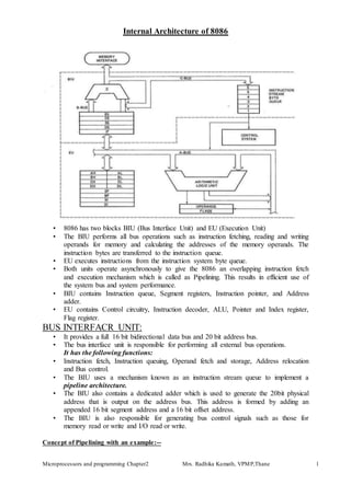
  • 1. Microprocessors and programming Chapter2 Mrs. Radhika Kamath, VPMP,Thane 1 Internal Architecture of 8086 • 8086 has two blocks BIU (Bus Interface Unit) and EU (Execution Unit) • The BIU performs all bus operations such as instruction fetching, reading and writing operands for memory and calculating the addresses of the memory operands. The instruction bytes are transferred to the instruction queue. • EU executes instructions from the instruction system byte queue. • Both units operate asynchronously to give the 8086 an overlapping instruction fetch and execution mechanism which is called as Pipelining. This results in efficient use of the system bus and system performance. • BIU contains Instruction queue, Segment registers, Instruction pointer, and Address adder. • EU contains Control circuitry, Instruction decoder, ALU, Pointer and Index register, Flag register. BUS INTERFACR UNIT: • It provides a full 16 bit bidirectional data bus and 20 bit address bus. • The bus interface unit is responsible for performing all external bus operations. It has the following functions: • Instruction fetch, Instruction queuing, Operand fetch and storage, Address relocation and Bus control. • The BIU uses a mechanism known as an instruction stream queue to implement a pipeline architecture. • The BIU also contains a dedicated adder which is used to generate the 20bit physical address that is output on the address bus. This address is formed by adding an appended 16 bit segment address and a 16 bit offset address. • The BIU is also responsible for generating bus control signals such as those for memory read or write and I/O read or write. Concept of Pipelining with an example:--
  • 2. Microprocessors and programming Chapter2 Mrs. Radhika Kamath, VPMP,Thane 2 • The BIU uses a mechanism known as an instruction stream queue to implement a pipeline architecture. o This queue permits prefetch of up to six bytes of instruction code. When ever the queue of the BIU is not requesting it to read or write operands from memory, the BIU is free to look ahead in the program by prefetching the next sequential instruction. o These prefetching instructions are held in its FIFO queue. With its 16 bit data bus, the BIU fetches two instruction bytes in a single memory cycle. o The EU accesses the queue from the output end. It reads one instruction byte after the other from the output of the queue. Concept of pipelining can be explained with the help of an example, where three instructions need to executed by the processor. On a non-pipelined processor, nine clock cycles are required for the individual fetch, decode and execute cycles for three instructions as shown below. Diagram given in class On a pipelined processor, where fetch, decode and execute operations are done in parallel, only five cycles are required as shown below. Diagram given in class Thus there is a tremendous performance gain in pipelined processors. Memory Segmentation :-- o The memory in an 8086 microprocessor is organized as a segmented memory.The physical memory is divided into 4 segments namely, Data Segment, Code segment, Stack segment and extra segment. Data segment is used to hold data, Code segment for the executable program, Extra segment also holds data specifically in strings and stack segment is used to store stack data. Each segment is 64Kbytes & addressed by one segment register. The segment registers for four segments are DS register, CS register, ES register & SS register. The 16 bit segment register holds the starting address of the segment. Since the memory size of 8086 is 1Mbytes, total 16 segments are possible with each having 64Kbytes o The physical address of the memory can range from 00000 to FFFFFH. The offset address to the segment address is specified as a 16-bit displacement between 0000 to FFFFH.. The following fig shows the memory segmentation, the base address is the starting address of the segment (Diagram given in class) Advantages of segmentation :-- o Though 8086 has 20 bit address, only 16 bits are sufficient to locate a memory location o Programs and data can be stored separately o By using more than one data or code segements, a large program can eb executed. o Useful in multi user time-shared system o Programs are position independent and re-locatable o Data can be shared by two processes o Addressability of a processor can be extended.
  • 3. Microprocessors and programming Chapter2 Mrs. Radhika Kamath, VPMP,Thane 3 o . The 16 bit offset or displacement is added to the 16 bit segment base register after the shifting the contents towards left by one digit to get 20 bits physical address. Physical memory address generation :-- • The 8086 memory has 220 addressable locations, with the help of 16 bits address, though it has a 20 bit address bus. • This is possible in the BIU which contains a dedicated adder used to generate the 20bit physical address which is theoutput on the address bus. This address is formed by adding an appended 16 bit segment address and a 16 bit offset address. This is generally shown as given below. Physical address generation for code segment :-- • CS register is used to hold the 16bit base address of Code segment. • The IP register is used to hold the 16 bit address of the next byte within the code segment. This is the offset or the displacement for CS register. • The physical address of the next instruction to be fetched is formed by combining the current contents of the code segment CS register and the current contents of the instruction pointer IP register. • For e.g., If CS = 3000H, and IP = 1234H, the physical address can be generated as given below Steps for the address generation:
  • 4. Microprocessors and programming Chapter2 Mrs. Radhika Kamath, VPMP,Thane 4  The 20 bit physical address can be represented as CS:IP for code segment.  CS is shifted to left by 4 bit positions (1 digit position) as 30000H, which is the base address for CS segment  Add IP i.e., 1234H to this base address to obtain 31234H, which is the 20 bit physical address. Physical address generation for code segment :-- • SS register is used to hold the 16bit base address of Stack segment. • The SP register is used to hold the 16 bit starting address of the segment where the word was most recently stored on the stack. This is called the Top of the stack. • The physical address of the stack while reading or writing is formed by combining the current contents of the stack segment SS register and the current contents of the stack pointerSP register. • For e.g., If SS = 5000H, and SP = 58F4H, the physical address can be generated as given below Steps for the address generation :  The 20 bit physical address can be represented as SS:SP for stack segment.  SS is shifted to left by 4 bit positions (1 digit position) as 50000H, which is the base address for SS segment  Add SP i.e., 58F4H to this base address to obtain 55F84H, which is the 20 bit physical address. EXECUTION UNIT • The Execution unit is responsible for decoding and executing all instructions. • The EU extracts instructions from the top of the queue in the BIU, decodes them, generates operands if necessary, passes them to the BIU and requests it to perform the read or write bys cycles to memory or I/O and perform the operation specified by the instruction on the operands. • During the execution of the instruction, the EU tests the status and control flags and updates them based on the results of executing the instruction. • If the queue is empty, the EU waits for the next instruction byte to be fetched and shifted to top of the queue. • When the EU executes a branch or jump instruction, it transfers control to a location corresponding to another set of sequential instructions. • Whenever this happens, the BIU automatically resets the queue and then begins to fetch instructions from this new location to refill the queue. • EU has a 16 bit ALU, which can perform arithmetic and logical operations on 8 bit as well as 16 bit data. • Flagregister is a 16-bit register containing 9 one bit flags. 1. Overflow Flag (OF) - set if the result is too large positive number, or is too small negative number to fit into destination operand. 2. Direction Flag (DF) - if set then string manipulation instructions will auto- decrement index registers. If cleared then the index registers will be auto- incremented. 3. Interrupt-enable Flag (IF) - setting this bit enables maskable interrupts. 4. Single-step Flag (TF) - if set then single-step interrupt will occur after the next instruction.
  • 5. Microprocessors and programming Chapter2 Mrs. Radhika Kamath, VPMP,Thane 5 5. Sign Flag (SF) - set if the most significant bit of the result is set. 6. Zero Flag (ZF) - set if the result is zero. 7. Auxiliary carry Flag (AF) - set if there was a carry from or borrow to bits 0-3 in the AL register. 8. Parity Flag (PF) - set if parity (the number of "1" bits) in the low-order byte of the result is even. 9. Carry Flag (CF) - set if there was a carry from or borrow to the most significant bit during last result calculation. Internal Registers of 8086 • The 8086 has four groups of the user accessible internal registers. They are the instruction pointer (IP), four data registers, four pointer and index register, four segment registers. • The 8086 has a total of fourteen 16-bit registers including a 16 bit register called the flag register, with 9 of bits implemented for status and control flags. • Most of the registers contain data/instruction offsets within 64 KB memory segment. There are four different 64 KB segments for instructions, stack, data and extra data. To specify where in 1 MB of processor memory these 4 segments are located the processor uses four segment registers: • Code segment (CS) is a 16-bit register containing address of 64 KB segment with processor instructions. The processor uses CS segment for all accesses to instructions referenced by instruction pointer (IP) register. CS register cannot be changed directly. The CS register is automatically updated during far jump, far call and far return instructions. • Stack segment (SS) is a 16-bit register containing address of 64KB segment with program stack. By default, the processor assumes that all data referenced by the stack pointer (SP) and base pointer (BP) registers is located in the stack segment. SS register can be changed directly using POP instruction. • Data segment (DS) is a 16-bit register containing address of 64KB segment with program data. By default, the processor assumes that all data referenced by general registers (AX, BX, CX, DX) and index register (SI, DI) is located in the data segment. DS register can be changed directly using POP and LDS instructions. • Accumulator register consists of two 8-bit registers AL and AH, which can be combined together and used as a 16-bit register AX. AL in this case contains the low-order byte of the word, and AH contains the high-order byte. Accumulator can be used for I/O operations and string manipulation. • Base register consists of two 8-bit registers BL and BH, which can be combined together and used as a 16-bit register BX. BL in this case contains the low-order byte of the word, and BH contains the high-order byte. BX register usually contains a data pointer used for based, based indexed or register indirect addressing. • Count register consists of two 8-bit registers CL and CH, which can be combined together and used as a 16-bit register CX. When combined, CL register contains the low- order byte of the word, and CH contains the high-order byte. Count register can be used in Loop, shift/rotate instructions and as a counter in string manipulation,. • Data register consists of two 8-bit registers DL and DH, which can be combined together and used as a 16-bit register DX. When combined, DL register contains the low-order byte of the word, and DH contains the high-order byte. Data register can be used as a port number in I/O operations. In integer 32-bit multiply and divide instruction the DX register contains high-order word of the initial or resulting number. The following registers are pointer and index registers:
  • 6. Microprocessors and programming Chapter2 Mrs. Radhika Kamath, VPMP,Thane 6 • Stack Pointer (SP) is a 16-bit register pointing to program stack. • Base Pointer (BP) is a 16-bit register pointing to data in stack segment. BP register is usually used for based, based indexed or register indirect addressing. • Source Index (SI) is a 16-bit register. SI is used for indexed, based indexed and register indirect addressing, as well as a source data address in string manipulation instructions. • Destination Index (DI) is a 16-bit register. DI is used for indexed, based indexed and register indirect addressing, as well as a destination data address in string manipulation instructions. 8086 Modes of operation :-- 8284 clock generator :-- refer class notes IC245 Bidirectional Buffer • Also called as Octal bus Transceiver • Bidirectional bus increases the current driving capacity of data bus • Each buffer can sink 24mA and source 15mA. • Consists of 16 non inverting buffers, eight for each direction with tri-state outputs. • G is the enable pin, when G=0,DIR is chosen. • Direction of data pin decided by DIR pin • When DIR = 1, Data A bus  B bus • When DIR =0, Data B bus  A bus IC373 Octal latch • Used for the separation of valid addresses from address/data bus • Controlled by the ALE signal of microprocessor • Latch is controlled by E input (STB input) which is connected to the clock input of D f/f. • Buffer is controlled by OE pin General Bus Operation: • The 8086 has a combined address and data bus commonly referred as a time multiplexed address and data bus. • The main reason behind multiplexing address and data over the same pins is the maximum utilisation of processor pins and it facilitates the use of 40 pin standard DIP package. • The bus can be demultiplexed using a few latches and transreceivers, when ever required. • Basically, all the processor bus cycles consist of at least four clock cycles. These are referred to as T1, T2, T3, T4. The address is transmitted by the processor during T1. It is present on the bus only for one cycle.
  • 7. Microprocessors and programming Chapter2 Mrs. Radhika Kamath, VPMP,Thane 7 • The negative edge of this ALE pulse is used to separate the address and the data or status information. In maximum mode, the status lines S0, S1 and S2 are used to indicate the type of operation. • Status bits S3 to S7 are multiplexed with higher order address bits and the BHE signal. Address is valid during T1 while status bits S3 to S7 are valid during T2 through T4. Minimum Mode 8086 System • In a minimum mode 8086 system, the microprocessor 8086 is operated in minimum mode by strapping its MN/MX pin to logic 1. • In this mode, all the control signals are given out by the microprocessor chip itself. There is a single microprocessor in the minimum mode system. • The remaining components in the system are latches, transreceivers, clock generator, memory and I/O devices. Some type of chip selection logic may be required for selecting memory or I/O devices, depending upon the address map of the system. • Latches are generally buffered output D-type flip-flops like 74LS373 or 8282. They are used for separating the valid address from the multiplexed address/data signals and are controlled by the ALE signal generated by 8086. • Transceivers are the bidirectional buffers and some times they are called as data amplifiers. They are required to separate the valid data from the time multiplexed address/data signals. • They are controlled by two signals namely, DEN and DT/R. • The DEN signal indicates the direction of data, i.e. from or to the processor. The system contains memory for the monitor and users program storage.
  • 8. Microprocessors and programming Chapter2 Mrs. Radhika Kamath, VPMP,Thane 8 • The working of the minimum mode configuration system can be better described in terms of the timing diagrams rather than qualitatively describing the operations. • The opcode fetch and read cycles are similar. Hence the timing diagram can be categorized in two parts, the first is the timing diagram for read cycle and the second is the timing diagram for write cycle. Minimum Mode Read bus cycle • The read cycle begins in T1 with the assertion of address latch enable (ALE) signal and also M / IO signal. During the negative going edge of this signal, the valid address is latched on the local bus. • The BHE and A0 signals address low, high or both bytes. From T1 to T4 , the M/IO signal indicates a memory or I/O operation. • At T2, the address is removed from the local bus and is sent to the output. The bus is then tristated. The read (RD) control signal is also activated in T2. • The read (RD) signal causes the address device to enable its data bus drivers. After RD goes low, the valid data is available on the data bus. • The addressed device will drive the READY line high. When the processor returns the read signal to high level, the addressed device will again tristate its bus drivers.
  • 9. Microprocessors and programming Chapter2 Mrs. Radhika Kamath, VPMP,Thane 9 Minimum Mode Write bus cycle • A write cycle also begins with the assertion of ALE and the emission of the address. The M/IO signal is again asserted to indicate a memory or I/O operation. In T2, after sending the address in T1, the processor sends the data to be written to the addressed location. • The data remains on the bus until middle of T4 state. The WR becomes active at the beginning of T2 (unlike RD is somewhat delayed in T2 to provide time for floating). • The BHE and A0 signals are used to select the proper byte or bytes of memory or I/O word to be read or write. • The M/IO, RD and WR signals indicate the type of data transfer as specified in table below. Maximum Mode 8086 System
  • 10. Microprocessors and programming Chapter2 Mrs. Radhika Kamath, VPMP,Thane 10 • In a maximum mode 8086 system, the microprocessor 8086 is operated in maximum mode bystrapping the MN/MX pin to ground. • In this mode, the processor derives the status signal S2, S1, S0. Another chip called bus controller derives the control signal using this status information. • In the maximum mode, there may be more than one microprocessor in the system configuration. • The components in the system are same as in the minimum mode system. • The basic function of the bus controller chip IC8288, is to derive control signals like RD and WR ( for memory and I/O devices), DEN, DT/R, ALE etc. using the information by the processor on the status lines. • The bus controller chip has input lines S2, S1, S0 and CLK. These inputs to 8288 are driven by CPU. • It derives the outputs ALE, DEN, DT/R, MRDC, MWTC, AMWC, IORC, IOWC and AIOWC. The AEN, IOB and CEN pins are specially useful for multiprocessor systems. • AEN and IOB are generally grounded. CEN pin is usually tied to +5V. The significance of the MCE/PDEN output depends upon the status of the IOB pin. • If IOB is grounded, it acts as master cascade enable to control cascade 8259A, else it acts as peripheral data enable used in the multiple bus configurations. • INTA pin used to issue two interrupt acknowledge pulses to the interrupt controller or to an interrupting device. • IORC, IOWC are I/O read command and I/O write command signals respectively. These signals enable an IO interface to read or write the data from or to the address port. • The MRDC, MWTC are memory read command and memory write command signals respectively and may be used as memory read or write signals. • All these command signals instructs the memory to accept or send data from or to the bus. • For both of these write command signals, the advanced signals namely AIOWC and AMWTC are available.
  • 11. Microprocessors and programming Chapter2 Mrs. Radhika Kamath, VPMP,Thane 11 Maximum mode Read bus cycle operation • Here the only difference between in timing diagram between minimum mode and maximum mode is the status signals used and the available control and advanced command signals. • R0, S1, S2 are set at the beginning of bus cycle.8288 bus controller will output a pulse as on the ALE and apply a required signal to its DT / R pin during T1. • In T2, 8288 will set DEN=1 thus enabling transceivers, and for an input it will activate MRDC or IORC. These signals are activated until T4. For an output, the AMWC or AIOWC is activated from T2 to T4 and MWTC or IOWC is activated from T3 to T4. • The status bit S0 to S2 remains active until T3 and become passive during T3 and T4. • If reader input is not activated before T3, wait state will be inserted between T3 and T4. Maximum mode Write Bus cycle