2. 2
Contents Page .No
Introduction to microcomputer
1 Microcomputer ………………………………………… 5
1.1 Buses …………………………………………………... 6
1.2 Memory ………………………………………………... 7
1.3 Timing ……………………………………………….. 12
1.4 CPU registers ………………………………………….. 12
2 Microprocessor architecture …………………………… 17
2.1 Pin diagram 17
2.2 Memory 22
2.3 Initialization …………………………………………… 26
2.4 Operation codes ……………………………………….. 30
2.5 Program counter ……………………………………….. 31
2.6 Branch and Jump instructions …………………………. 31
2.8 Subroutine ……………………………………………... 32
3 3.1 Analog to digital converters …………………………… 32
3.2 Flash ADC 34
3.4 Digital to analog converters …………………………… 34
3.3 Sampling ………………………………………………. 36
3.4 Polling and Interrupts ………………………………….. 37
3.5 Digital filters ………………………………………….. 39
4 Lookup table …………………………………………... 41
Sensors and actuators
2 2.1 Speed sensors ………………………………………… 43
3. 3
2.2 Pressure sensors …………………………………………… 44
2.2.1 Manifold Absolute Pressure sensor ……………………….. 45
3 Knock sensor ……………………………………………… 48
4 Temperature sensors ……………………………………… 49
4.1 Coolant and Exhaust gas temperature …………………… 50
4.2 Exhaust Oxygen level sensor ……………………………… 52
5 Position sensors …………………………………………… 62
5.1 Throttle position sensor …………………………………… 63
5.2 Accelerator pedal position sensor ………………………… 66
5.3 Crankshaft position sensor ……………………………… 67
6 Air mass flow sensor ……………………………………… 69
7 Solenoids ………………………………………………… 71
8 Stepper motors …………………………………………… 73
9 Relays …………………………………………………… 75
4. 4
Unit I Introduction to microcomputer
Microcomputer: Buses, memory, timing, CPU registers; Microprocessor architecture:
Initialization, operation codes, program counter, branch and jump instructions,
subroutine. Analog to digital converters and Digital to analog converters, sampling,
polling and interrupts, digital filters, lookup table.
5. 5
Unit I - Introduction to microcomputer
1. Microcomputer:
A microcomputer is just a small computer, typically thousands of times smaller than the
large, general-purpose mainframe computers used by banks and large corporations. Microcomputers
cost much less than mainframes, and their computing power and speed is only a fraction of that of a
mainframe. A typical mainframe computer costs from tens of thousands of dollars to millions of
dollars and is capable of hundreds of thousands of arithmetic operations per second (additions,
subtractions, multiplications, and divisions).
A microcomputer costs from a little less than $1,000 to $15,000 and can perform several
thousand operations per second. More important for mathematical calculations than the speed of the
operation is the accuracy of the operation. Mainframe computers use up to 64 bits to obtain high
accuracy when doing arithmetic. The decimal equivalent for the largest number that can be
represented using 64 bits is roughly 10 to the 19th power (1 followed by 19 zeros). A typical engine
control microcomputer does arithmetic using only 16–32 bits. The largest decimal number that can
be represented in 8 bits is 127, if one of the bits is used as a sign bit to indicate whether the number
is positive or negative.
The term microcomputer is generally synonymous with personal computer (PC), or a
computer that depends on a microprocessor. Microcomputers are designed to be used by
individuals, whether in the form of PCs, workstations or notebook computers. A microcomputer
contains a central processing unit (CPU) on a microchip (the microprocessor), a memory system
(typically read-only memory and random access memory), a bus system and I/O ports, typically
housed in a motherboard.
Fig 1 – Micro Computer
6. 6
Microcomputer Components
1. Buses:
The physical connections that carry control information between the CPU and other devices within
the computer.
1.1 System Bus
The three components of the microcomputer system is connected by three busses, also known as
system bus. These busses are used to transfer information (data) internally and externally to the
microprocessor.
1.1.1 Address Bus
The address bus is 'unidirectional', over which the microprocessor sends an address code to the
memory or input/output. The size (width) of the address bus is specified by the number of bits it can
handle. The more bits there are in the address bus, the more memory locations a microprocessor can
access. A 16 bit address bus is capable of addressing 65,536 (64K) addresses.
1.1.2 Data Bus
The data bus is 'bi-directional', on which data or instruction codes are transferred into the
microprocessor or on which the result of an operation or computation is sent out from the
microprocessor to the memory or input/ output. Depending on the particular microprocessor, the
data bus can handle 8 bit or 16 bit data.
1. 1.3 Control Bus
The control bus is used by the microprocessor to send out or receive timing and control signals in
order to coordinate and regulate its operation and to communicate with other devices, i.e. memory
7. 7
or input/output. The lines used to control memory and I/O devices are MEMRQ*, IORQ*, RD* and
WR*. Others are general control signals to handle special external requests (interrupts) special I/O
devices (DMA) and special kind of memory (DRAM).
1.2 Memory:
1.2.1 Primary Memory
A microcomputer would be incapable of performing even the simplest task if it did not contain
some type of memory. Consider an example where want the microcomputer to add the numbers 2
and 2. When you type the first 2 in from the keyboard, the CPU does not yet know what intend to
do with it so it has to store the number. When you enter the plus sign it now knows you intend to do
some arithmetic but it still needs another number. Finally, enter the second 2 and the CPU performs
the calculation and stores the result in memory. A microcomputer uses memory to store the
programs that control its operation, to store data waiting for processing, and to store the results of
operations performed by the CPU.
Primary memory, or storage, is electronic memory that is directly addressable by the CPU. This
memory is contained in integrated circuits called memory chips. Each memory location is assigned
a number called an address. The CPU uses these addresses to keep track of information stored in
memory. Since primary memory is completely electronic, transfer of data to and from it is
extremely fast. A microcomputer contains several types of primary memory. RAM (Random
Access Memory) is used for storing information that changes frequently. This is the memory in a
computer that is accessible to the user. RAM is used to store user programs that control what the
CPU does. It stores the data used by these programs and the results of operations performed by
these programs. How much RAM a computer has determines the size and sophistication of the tasks
a microcomputer can perform. This is the memory in a microcomputer that is normally referenced
in the computer’s specifications. Today’s microcomputers typically have 32 MB or more of RAM.
RAM is an example of volatile memory. This means that everything stored in RAM is lost when the
power is turned off - even for an instant.
RAM memory chips are usually found as part of a SIMM (Single In-line Memory Module) or a
DIMM (Dual In-line Memory Module). SIMMs and DIMMs are small circuit boards containing
RAM memory chips. These circuit boards plug into special sockets located on the motherboard of
the microcomputer. SIMMs have 72 pins on the connector edge of the circuit board and support 32-
bit memory transfers (32-bit memory bus). DIMMs have 168 connectors and support 64-bit
8. 8
memory transfers. A SIMM and DIMM are shown in Figure 1.17. Click here for a video clip
showing the installation of a SIMM module (Format: RealVideo; Size: 200 K).
Figure: 72-pin SIMM (top) and 168-pin DIMM (bottom)
Another type of memory found in all microcomputers is ROM (Read Only Memory). ROM can be
read by the user but cannot be altered. ROM is nonvolatile which means it retains the information
stored in it even when the power is turned off. ROM is used primarily to store the instructions a
microcomputer needs to get itself started after turn on the power. These instructions are called the
BIOS (Basic Input/ Output System). This start up process is called booting or bootstrapping and
figuratively means that the computer pulls itself up by its own bootstraps. The BIOS is placed in
ROM by the computer manufacturer and cannot be altered by the user.
Examples of other kinds of memory chips include, PROM, EPROM, and EEPROM. PROM
(Programmable Read Only Memory) is a type of ROM that can be programmed by the user.
However, once it is programmed, the contents cannot be changed. The ROM chip in a
microcomputer starts out as a PROM chip. After being programmed by the manufacturer, it can
only be read, not written to again. EPROM (Erasable Programmable Read Only Memory) is a type
of PROM chip that can be erased and reprogrammed. An EPROM chip is erased by shining
ultraviolet light on it through a quartz window located on top of the chip. A diagram of an EPROM
chip is shown in Figure 1.18. EEPROM (Electronically Erasable Programmable Read Only
Memory) is much like EPROM except that EEPROM chips can be erased by an electrical signal
instead of ultraviolet light.
9. 9
Figure: EPROM Chip
In addition to their use in microcomputers, EEPROM chips are used in a variety of household
devices that must retain programmed settings such a televisions, clocks, camera, and automotive
control systems.
1.2.2 ROM (Read Only Memory)
ROMs are the memory devices that retain its data even if the power is disconnected. It is generally
used as the system or monitor programs to process the power on reset in computers.
1.2 3 Mask-programmable ROM (or mask ROM)
ROMs are programmed by the pattern of connections and no connections in one of masks used in
the IC manufacturing process. To program or write information in to the ROM, the customer gives
the manufacturer a listing of the ROM contents, using a floppy disk or other medium. The
manufacturer uses this information to create one or more customized masks to manufacture ROMs
with the required pattern.
Programmable Read Only Memory (PROM)
1.2.4 Programmable Read Only Memory (PROM)
It is a one-time writeable by a PROM programmer. A PROM is manufactured with all of its diodes
or transistors connected. This corresponds to having all bits at a particular value, typically 1. The
PROM programmer can be used to set desired bits to opposite value (typically 0), by vaporizing
tiny fusible links inside the PROM corresponding to each bit. A link is vaporized by selecting it
using the PROM’s address and data lines, and then applying a high-voltage pulse (10 to 30V) to the
device through a special input pin.
10. 10
1.2.5 Erasable PROM (EPROM)
It is programmed like a PROM, but it can also be erased to the all-1's state by exposing it to
ultraviolet light. Each transistor has two gates, floating and non-floating. The floating gate is
unconnected and is surrounded by extremely high-impedance insulating material. To program an
EPROM, the programmer applies a high voltage to the non-floating gate at each bit location where
a ‘0' is to be stored. This causes a breakdown in the insulating material and allows a negative charge
to accumulate on the floating gate. When the high voltage is removed, the negative charge remains.
During the subsequent read operation, the negative charge prevents the MOS transistor from turning
on when it is selected. The insulating material surrounding the floating gate becomes slightly
conductive if it is exposed to ultra violet light with a certain wave length. Thus. EPROMs can be
erased by exposing the chips to ultraviolet light, typically for 5-20 minutes.
1.2.6 Electrically Erasable PROM (EEPROM)
It is similar to EPROM except that individual stored bits may be erased electrically. The floating
gates in an EEPROM are surrounded by a much thinner insulating layer, and can be erased by
applying a voltage of the opposite polarity as the charging voltage to the non-floating gate.
1.2.7 RAM (Random Access Memory)
Data can be read or written to RAM without any special voltages or light source. A data word in the
memory is typically read or written one word at a time after selecting the address of it. However,
the data stored in RAM is lost if the power to the IC chip is disconnected.
1.2.8 Static RAM (SRAM)
The information remains stored as long as power is applied to the chip, unless the same location is
written again.
1.2. 10 Dynamic RAM (DRAM)
The data stored at each location must be periodically refreshed by reading it and the writing it back
again, or else it disappears. DRAM is by far the cheapest to build. Newer and faster DRAM types
are developed continuously.
Currently, there are at least four types:
FPM (Fast Page Mode)
ECC (Error Correcting Code)
EDO (Extended Data Output)
SDRAM (Synchronous Dynamic RAM)
1.2.10.1 A brief explanation of DRAM types
11. 11
FPM was the traditional RAM for PCs, before the EDO was introduced. It is mounted in SIMM
modules of 2, 4, 8, 16, or 32 MB. Typically, it is found in 60 ns or 70 ns versions. 60 ns is the
fastest and the one to use. cannot mix different speeds on the same Pentium motherboard.
EDO is an improvement of FPM RAM. EDO stands for “Extended Data Out” which means the chip
asserts the data on its output pins longer (probably under special hardware handshaking), even
while the next requested address is strobed into the address lines. It makes memory access faster
because can do the addressing and reading concurrently. By switching from FPM to EDO, one can
expect a performance improvement of 2 to 5 percent. EDO RAM is usually sold in 60 ns versions.
A 50 ns version is available at higher cost.
ECC RAM is a special error correcting RAM type. It is especially used in servers.
Synchronous DRAM (SDRAM) is a generic name for various kinds of DRAM that are
synchronized with the clock speed that the microprocessor is optimized for. This tends to increase
the number of instructions that the processor can perform in a given time. The speed of SDRAM is
rated in MHz rather than in nanoseconds (ns).
This makes it easier to compare the bus speed and the RAM chip speed. can convert the RAM clock
speed to nanoseconds by dividing the chip speed into 1 billion ns (which is one second). For
example, an 83
MHz RAM would be equivalent to 12 ns. It comes only in 64 bit modules (long 168 pin DIMMs).
RAMBUS Dynamic Random Access Memory (RDRAM) is a future RAM type. Intel and others
have great expectations from this type. RDRAM promises to transfer up to 1.6 billion bytes per
second. The subsystem consists of the RAM, the RAM controller, and the bus (path) connecting
RAM to the microprocessor and devices in the computer that use it. Direct Rambus (DRDRAM), a
technology developed and licensed by the Rambus Corporation, will be used with Intel
microprocessors beginning in 1999. High-speed RAM is expected to accelerate the growth of
visually intensive interfaces such as 3-D, interactive games, and streaming multimedia. Rambus is
intended to replace the current main memory technology of dynamic random access memory
(DRAM). Much faster data transfer rates from attached devices such as videocams using Firewire
and the Accelerated Graphics Port (AGP) make it important to reduce the bottleneck in getting data
into the computer, staging it in RAM, and moving it throught the microprocessor and to the display
or other output devices.
12. 12
1.3 Timing:
A certain amount of time is required for the memory’s address decoder to decode which memory
location is called for by the address, and also for the selected memory location to transfer its
information to the data bus. To allow time for this decoding, the processor waits a while before
receiving the information requested from the data bus. Then, at the proper time, the CPU opens the
logic gating circuitry between the data bus and the CPU data register so that the information on the
bus from memory location 10 is latched into the CPU. During the memory read operation, the
memory has temporary control of the data bus. Control must be returned to the CPU, but not before
the processor has read in the data. The CPU provides a timing control signal, called the clock, that
tells the memory when it can take and release control of the data bus.
Refer again to Figure . Notice that the read cycle is terminated when the clock goes from high to
low during the time that the read signal is valid. This is the signal the CPU uses to tell the memory
that it has read the data and the data bus can be released. The timing for a memory write operation
is very similar to the memory read operation except that the R/W line is low instead of high. The
bus timing signals are very important to the reliable operation of the computer. However, they are
built into the design of the machine and, therefore, are under machine control. As long as the
machine performs the read and write operations correctly, the programmer can completely ignore
the details of the bus timing signals and concentrate on the logic of the program.
1.4 CPU Registers:
In computer architecture, a processor register is a small amount of storage available as part of a
CPU or other digital processor. Such registers are (typically) addressed by mechanisms other than
main memory and can be accessed more quickly. Almost all computers, load-store architecture or
not, load data from a larger memory into registers where it is used for arithmetic, manipulated, or
13. 13
tested, by some machine instruction. Manipulated data is then often stored back in main memory,
either by the same instruction or a subsequent one. Modern processors use either static or dynamic
RAM as main memory, the latter often being implicitly accessed via one or more cache levels. A
common property of computer programs is locality of reference: the same values are often accessed
repeatedly and frequently used values held in registers improves performance. This is what makes
fast registers (and caches) meaningful.
Processor registers are normally at the top of the memory hierarchy, and provide the fastest way to
access data. The term normally refers only to the group of registers that are directly encoded as part
of an instruction, as defined by the instruction set. However, modern high performance CPUs often
have duplicates of these "architectural registers" in order to improve performance via register
renaming, allowing parallel and speculative execution. Modern x86 is perhaps the most well known
example of this technique.
Allocating frequently used variables to registers can be critical to a program's performance. This
register allocation is either performed by a compiler, in the code generation phase, or manually, by
an assembly language programmer.
1.4.1 Categories of registers
Registers are normally measured by the number of bits they can hold, for example, an "8-bit
register" or a "32-bit register". A processor often contains several kinds of registers, that can be
classified accordingly to their content or instructions that operate on them:
User-accessible Registers – The most common division of user-accessible registers is into data
registers and address registers.
Data registers can hold numeric values such as integer and floating-point values, as well as
characters, small bit arrays and other data. In some older and low end CPUs, a special data register,
known as the accumulator, is used implicitly for many operations.
Address registers hold addresses and are used by instructions that indirectly access primary
memory.
Some processors contain registers that may only be used to hold an address or only to hold numeric
values (in some cases used as an index register whose value is added as an offset from some
address); others allow registers to hold either kind of quantity. A wide variety of possible
addressing modes, used to specify the effective address of an operand, exist.
The stack pointer is used to manage the run-time stack. Rarely, other data stacks are addressed by
dedicated address registers, see stack machine.
14. 14
Conditional registers hold truth values often used to determine whether some instruction should or
should not be executed.
General purpose registers (GPRs) can store both data and addresses, i.e., they are combined
Data/Address registers.
1.4.2 Floating point registers (FPRs) store floating point numbers in many architectures.
Constant registers hold read-only values such as zero, one, or pi.
Vector registers hold data for vector processing done by SIMD instructions (Single Instruction,
Multiple Data).
1.4.3 Special purpose registers ( SPR ) hold program state; they usually include the program
counter (aka instruction pointer) and status register (aka processor status word). The
aforementioned stack pointer is sometimes also included in this group. Embedded microprocessors
can also have registers corresponding to specialized hardware elements.
Instruction register store the instruction currently being executed.
In some architectures, model-specific registers (also called machine-specific registers) store data
and settings related to the processor itself. Because their meanings are attached to the design of a
specific processor, they cannot be expected to remain standard between processor generations.
Control and status registers – It has three types: program counter, instruction registers and program
status word (PSW).
Registers related to fetching information from RAM, a collection of storage registers located on
separate chips from the CPU (unlike most of the above, these are generally not architectural
registers):
1.4.4 Memory buffer register
A Memory Buffer Register (MBR) is the register in a computer's processor, or central processing
unit, CPU, that stores the data being transferred to and from the immediate access store. It acts as a
buffer allowing the processor and memory units to act independently without being affected by
minor differences in operation. A data item will be copied to the MBR ready for use at the next
clock cycle, when it can be either used by the processor or stored in main memory.
This register holds the contents of the memory which are to be transferred from memory to other
components or vice versa. A word to be stored must be transferred to the MBR, from where it goes
to the specific memory location, and the arithmetic data to be processed in the ALU first goes to
MBR and then to accumulated register, and then it is processed in the ALU.
15. 15
1.4.5 Memory data register
The Memory Data Register (MDR) is the register of a computer's control unit that contains the data
to be stored in the computer storage (e.g. RAM), or the data after a fetch from the computer storage.
It acts like a buffer and holds anything that is copied from the memory ready for the processor to
use it.
The MDR is a 'a into memory.
The Memory Data Register is half of a minimal interface between a microprogram and computer
storage, the other half is a memory address register.
Far more complex memory interfaces exist, but this is the simplest that can work.
The Memory Data Register (MDR) contains the data value being fetched or stored. We might be
tempted to say that the MDR should be W bits wide, where W is the cell size. However on most
computers the cell size is only 8-bits, and most data values occupy multiple cells. Thus the size of
the MDR is usually a multiple of 8. Typical values of MDR width are 32 and 64 bits, which would
allow us to fetch, in a single step, either an integer or a real value.
For example, to retrieve the contents of cell 123, we would load the value 123 (in binary, of course)
into the MAR and perform a fetch operation. When the operation is done, a copy of the contents of
cell 123 would be in the MDR. To store the value 98 into cell 4, we load a 4 into the MAR and a 98
into the MDR and perform a store. When the operation is completed the contents of cell 4 will have
been set to 98, by discarding whatever was there previously.
1.4.6 Memory address register
The Memory Address Register (MAR) is a CPU register that either stores the memory address from
which data will be fetched to the CPU or the address to which data will be sent and stored.
In other words, MAR holds the memory location of data that needs to be accessed. When reading
from memory, data addressed by MAR is fed into the MDR (memory data register) and then used
by the CPU. When writing to memory, the CPU writes data from MDR to the memory location
whose address is stored in MAR.
The Memory Address Register is half of a minimal interface between a microprogram and computer
storage. The other half is a memory data register.
1.4.7 Memory Type Range Registers (MTRR)
Memory type range registers (MTRRs) are a set of processor supplementary capabilities control
registers that provide system software with control of how accesses to memory ranges by the CPU
16. 16
are cached. It uses a set of programmable model-specific registers (MSRs) which are special
registers provided by most modern CPUs.
Possible access modes to memory ranges can be:
uncached
write-through
write-combining
write-protect
write-back
Additional bits which are provided on some computer architectures such as AMD64 allow the
shadowing of ROM contents in system memory (Shadow ROM) and the configuration of memory-
mapped I/O.
In write-back mode, writes are written to the CPU's cache and the cache is marked dirty, so that its
contents are written to memory later.
Write-combining allows bus write transfers to be combined into a larger transfer before bursting
them over the bus to allow more efficient writes to system resources like graphics card memory.
This often increases the speed of image write operations by several times, at the cost of losing the
simple sequential read/write semantics of normal memory.
1.4.8 Hardware registers are similar, but occur outside CPUs.
In digital electronics, especially computing, a hardware register stores bits of information, in a way
that all the bits can be written to or read out simultaneously. The hardware registers inside a central
processing unit (CPU) are called processor registers. Signals from a state machine to the register
control when registers transmit to or accept information from other registers. Sometimes the state
machine routes information from one register through a functional transform, such as an adder unit,
and then to another register that stores the results.
Typical uses of hardware registers include configuration and start-up of certain features, especially
during initialization, buffer storage e.g. video memory for graphics cards, input/output (I/O) of
different kinds, and status reporting such as whether a certain event has occurred in the hardware
unit.
Reading a hardware register in "peripheral units" -- computer hardware outside the CPU—involves
accessing its memory-mapped I/O address or port-mapped I/O address with a "load" or "store"
instruction, issued by the processor. Hardware registers are addressed in words, but sometimes only
use a few bits of the word read in to, or written out to the register.
17. 17
Strobe registers have the same interface as normal hardware registers, but instead of storing data,
they trigger an action each time they are written to (or, in rare cases, read from). They are a means
of signaling.
Registers are normally measured by the number of bits they can hold, for example, an "8-bit
register" or a "32-bit register". Registers can be implemented in a wide variety of ways, including
register files, standard SRAM, individual flip-flops, or high speed core memory.
In addition to the "programmer-visible" registers that can be read and written with software, many
chips have internal microarchitectural registers that are used for state machines and pipelining; for
example, registered memory.
Commercial design tools such as Socrates Bitwise by Duolog Technologies, simplify and automate
memory-mapped register specification and code generation for hardware, firmware, hardware
verification, testing and documentation.
2. Microprocessor architecture
Introduction
In the previous articles we saw about the architecture of 8085 microprocessor. Now we have a
rough idea about how the instructions, data's are transferred and processed in 8085
microprocessor. In this article let us discuss in detail about the various signals involved in
transferring data and executing instructions in microprocessor.
2.1 Pin Diagram:
18. 18
2.1.1 Classification of Signals
The various signals in a microprocessor can be classified as Power supply and Frequency
signals: Signals which aids in supplying power and generating frequency are associated with
this type. Pins like Vcc and ground are classified under this type.
Address signals: Signals associated with the lower order address bus and time multiplexed
higher order address bus comes under this type of signals.
Data Signals: Signals associated with data bus comes under this type.
Control and Status Signals: Signals which are associated with timing and control unit such
HOLD, RW’, WR’ etc. comes under this type of signals.
Interrupt Signals: We know that signals like TRAP, RST 5.5 etc. are interrupt signals. Such
signals come under this category.
Serial I/O signals: These signals are used for giving serial input and output data. Signals like
SID, SOD come under this category.
Acknowledgement Signals: Signals like INTA’, HLDA acts as acknowledgement signal for
8085 microprocessor.
2.1.2 Address Bus:
The pins A8-A15 denote the address bus. They are used for the most significant bit of memory
address.
Address/Data Bus:
AD0-AD7 constitutes the Address/Data bus. They are time multiplexed. These pins are used for
least significant bits of address bus in the first machine clock cycle and used as data bus for
second and third clock cycle.
A clock cycle is nothing but the time taken between two adjacent pulses of the oscillator. In
19. 19
simple words clock cycle refers to the transition between o volts to 5 volts and back to 0 volts.
So the first clock cycle means the first transition of pulse from 0volts to 5 volts and then back to
0 volts.
2.1.3 ALE: Address Latch Enable:
In the previous article we saw how ALE helps in demultiplexing the lower order address and
data bus. This signal goes high during the first clock cycle and enables the lower order address
bits. The lower order address bus is added to memory or any external latch.
2.1.4 IO/M’:
Consider we have an address to be processed. But how do the processors know whether the
address is for memory or I/O functions? For this purpose a status signal called IO/M’ is used.
This distinguishes whether the address is for memory or IO. When this pin goes high, the
address is for an I/O device. While the pin goes low, the address is assigned for the memory.
2.1.5 S0-S1:
S0 and S1 are status signals which provides different status and functions depending on their
status.
2.1.6 RD’:
This is an active low signal. That is, an operation is performed when the signal goes low. This
signal is used to control READ operation of the microprocessor. When this pin goes low the
microprocessor reads the data from memory or I/O device.
2.1.7 WR’:
WR’ is also an active low signal which controls the write operations of the microprocessor.
When this pin goes low, the data is written to the memory or I/O device.
2.1.8 READY:
READY is used by the microprocessor to check whether a peripheral is ready to accept or
transfer data. A peripheral may be a LCD display or analog to digital converter or any other.
These peripherals are connected to microprocessor using the READY pin. If READY is high
then the periphery is ready for data transfer. If not the microprocessor waits until READY goes
high.
2.1.9 HOLD:
This indicates if any other device is requesting the use of address and data bus. Consider two
peripheral devices. One is the LCD and the other Analog to Digital converter. Suppose if analog
to digital converter is using the address and data bus and if LCD requests the use of address and
20. 20
data bus by giving HOLD signal, then the microprocessor transfers the control to the LCD as
soon as the current cycle is over. After the LCD process is over, the control is transferred back
to analog and digital converter.
2.1.10 HLDA:
HLDA is the acknowledgment signal for HOLD. It indicates whether the HOLD signal is
received or not. After the execution of HOLD request, HLDA goes low.
2.1.11 INTR:
INTR is an interrupt request signal. It has the lowest priority among the interrupts. INTR can be
enabled or disabled by using software. Whenever INTR goes high the microprocessor completes
the current instruction which is being executed and then acknowledges the INTR signal and
processes it.
2.1.12 INTA’:
Whenever the microprocessor receives interrupt signal. It has to be acknowledged. This
acknowledgement is done by INTA’. So whenever the interrupt is received INTA’ goes high.
2.1.13 RST 5.5, 6.5, 7.5:
These are nothing but the restart interrupts. They insert an internal restart function
automatically.
All the above mentioned interrupts are maskable interrupts. That is, they can be enabled or
disabled using programs.
2.1.14 TRAP:
Among the interrupts of 8085 microprocessor, TRAP is the only non-maskable interrupt. It
cannot be enabled or disabled using a program. It has the highest priority among the interrupts.
PRIORITY ORDER (From highest to lowest)
TRAP
RST 7.5
RST 6.5
RST 5.5
INTR
2.1.15 RESET IN’:
This pin resets the program counter to 0 and resets interrupt enable and HLDA flip-flops. The
CPU is held in reset condition until this pin is high. However the flags and registers won’t get
affected except for instruction register.
21. 21
2.1.16 RESET OUT:
This pin indicates that the CPU has been reset by RESET IN’.
2.1.17 X1 X2:
These are the terminals which are connected to external oscillator to produce the necessary and
suitable clock operation.
2.1.18 CLK:
Sometimes it is necessary for generating clock outputs from microprocessors so that they can be
used for other peripherals or other digital IC’s. This is provided by CLK pin. Its frequency is
always same as the frequency at which the microprocessor operates.
2.1.19 SID:
This pin provides serial input data. The serial data on this pin is loaded into the seventh bit of
the accumulator when RIM instruction is executed.
RIM stands for READ INTERRUPT MASK, which checks whether the interrupt is masked or
not.
2.1.20 SOD:
This pin provides the serial output data. The serial data on this pin delivers its output to the
seventh bit of the accumulator when SIM instruction is executed.
Vcc and Vss:
Vcc is +5v pin and Vss is ground pin.
22. 22
2.2 Memory
• Program, data and stack memories occupy the same memory space. The total
addressable memory size is 64 KB.
• Program memory - program can be located anywhere in memory. Jump, branch and call
instructions use 16-bit addresses, i.e. they can be used to jump/branch anywhere within 64
KB. All jump/branch instructions use absolute addressing.
• Data memory - the processor always uses 16-bit addresses so that data can be placed
anywhere.
• Stack memory is limited only by the size of memory. Stack grows downward.
• First 64 bytes in a zero memory page should be reserved for vectors used by RST
instructions.
23. 23
2.3 Interrupts
• The processor has 5 interrupts. They are presented below in the order of their priority
(from lowest to highest):
• INTR is maskable 8080A compatible interrupt. When the interrupt occurs the processor
fetches from the bus one instruction, usually one of these instructions:
• One of the 8 RST instructions (RST0 - RST7). The processor saves current program counter
into stack and branches to memory location N * 8 (where N is a 3-bit number from 0 to 7
supplied with the RST instruction).
• CALL instruction (3 byte instruction). The processor calls the subroutine, address of which
is specified in the second and third bytes of the instruction.
• RST5.5 is a maskable interrupt. When this interrupt is received the processor saves the
contents of the PC register into stack and branches to 2CH (hexadecimal) address.
• RST6.5 is a maskable interrupt. When this interrupt is received the processor saves the
contents of the PC register into stack and branches to 34H (hexadecimal) address.
• RST7.5 is a maskable interrupt. When this interrupt is received the processor saves the
contents of the PC register into stack and branches to 3CH (hexadecimal) address.
• TRAP is a non-maskable interrupt. When this interrupt is received the processor saves the
contents of the PC register into stack and branches to 24H (hexadecimal) address.
• All maskable interrupts can be enabled or disabled using EI and DI instructions. RST 5.5,
RST6.5 and RST7.5 interrupts can be enabled or disabled individually using SIM
instruction.
2.4 Reset Signals
• RESET IN: When this signal goes low, the program counter (PC) is set to Zero, µp is
reset and resets the interrupt enable and HLDA flip-flops.
• The data and address buses and the control lines are 3-stated during RESET and because
of asynchronous nature of RESET, the processor internal registers and flags may be
altered by RESET with unpredictable results.
• RESET IN is a Schmitt-triggered input, allowing connection to an R-C network for
power-on RESET delay.
• Upon power-up, RESET IN must remain low for at least 10 ms after minimum Vcc has
been reached.
• For proper reset operation after the power – up duration, RESET IN should be kept low
24. 24
a minimum of three clock periods.
• The CPU is held in the reset condition as long as RESET IN is applied. Typical Power-on
RESET RC values R1 = 75Kȍ, C1 = 1µF.
• RESET OUT: This signal indicates that µp is being reset. This signal can be used to reset
other devices. The signal is synchronized to the processor clock and lasts an integral
number of clock periods.
Serial communication Signal
• SID - Serial Input Data Line: The data on this line is loaded into accumulator bit 7
whenever a RIM instruction is executed.
• SOD – Serial Output Data Line: The SIM instruction loads the value of bit 7 of the
accumulator into SOD latch if bit 6 (SOE) of the accumulator is 1.
DMA Signals
• HOLD: Indicates that another master is requesting the use of the address and data buses.
The CPU, upon receiving the hold request, will relinquish the use of the bus as soon as the
completion of the current bus transfer.
• Internal processing can continue. The processor can regain the bus only after the HOLD is
removed.
• When the HOLD is acknowledged, the Address, Data RD, WR and IO/M lines are 3-stated.
• HLDA: Hold Acknowledge: Indicates that the CPU has received the HOLD request
and that it will relinquish the bus in the next clock cycle.
• HLDA goes low after the Hold request is removed. The CPU takes the bus one half-
clock cycle after HLDA goes low.
• READY: This signal Synchronizes the fast CPU and the slow memory,
peripherals.
• If READY is high during a read or write cycle, it indicates that the memory or
peripheral is ready to send or receive data.
• If READY is low, the CPU will wait an integral number of clock cycle for READY
to go high before completing the read or write cycle.
• READY must conform to specified setup and hold times.
Registers
• Accumulator or A register is an 8-bit register used for arithmetic, logic, I/O and
load/store operations.
25. 25
• Flag Register has five 1-bit flags.
• Sign - set if the most significant bit of the result is set.
• Zero - set if the result is zero.
• Auxiliary carry - set if there was a carry out from bit 3 to bit 4 of the result.
• Parity - set if the parity (the number of set bits in the result) is even.
• Carry - set if there was a carry during addition, or borrow during
subtraction/comparison/rotation.
2.5 General Registers
• 8-bit B and 8-bit C registers can be used as one 16-bit BC register pair. When used as a
pair the C register contains low-order byte. Some instructions may use BC register as a
data pointer.
• 8-bit D and 8-bit E registers can be used as one 16-bit DE register pair. When used as a
pair the E register contains low-order byte. Some instructions may use DE register as a
data pointer.
• 8-bit H and 8-bit L registers can be used as one 16-bit HL register pair. When used as a
pair the L register contains low-order byte. HL register usually contains a data pointer used
to reference memory addresses.
• Stack pointer is a 16 bit register. This register is always
decremented/incremented by 2 during push and pop.
• Program counter is a 16-bit register.
2.6 Instruction Set
• 8085 instruction set consists of the following instructions:
• Data moving instructions.
• Arithmetic - add, subtract, increment and decrement.
• Logic - AND, OR, XOR and rotate.
• Control transfer - conditional, unconditional, call subroutine, return from
subroutine and restarts.
• Input/Output instructions.
• Other - setting/clearing flag bits, enabling/disabling interrupts, stack operations, etc.
2.7 Addressing mode
• Register - references the data in a register or in a register pair.
26. 26
Register indirect - instruction specifies register pair containing address, where the data is
located.
Direct, Immediate - 8 or 16-bit data.
2.3 Initialization
Microprocessor initialization and configuration information for both uniprocessor and dual-
processor implementations of the embedded Pentium® processor family. For configuration
information on symmetric dual-processing mode, refer to “Managing and Designing with the
Symmetrical Dual Processing Configuration Before normal operation of the processor can begin,
the processor must be initialized by driving the RESET pin active. The RESET pin forces the
processor to begin execution in a known state. Several features are optionally invoked at the falling
edge of RESET: Built-in-Self-Test (BIST), Functional Redundancy Checking and Three-state Test
Mode. In addition to the standard RESET pin, the processor has implemented an initialization pin
(INIT) that allows the processor to begin execution in a known state without disrupting the contents
of the internal caches or the floating-point state. The embedded Pentium processor power up and
initialization procedures, and the test and configuration features enabled at the falling edge of
RESET.
2.3.1 Power Up Specifications
During power up, RESET must be asserted while VCC is approaching nominal operating voltage to
prevent internal bus contention, which could negatively affect the reliability of the processor.
It is recommended that CLK begin toggling within 150 ms after VCC reaches its proper operating
level. For the embedded Pentium® processor with MMX™ technology, it is recommended that the
CLK signal begin toggling within 150 ms after the last VCC plane stabilizes. This recommendation
is only to ensure long term reliability of the device. In order for RESET to be recognized, the CLK
input needs to be toggling. RESET must remain asserted for 1 millisecond after VCC and CLK
have reached their AC/DC specifications.
2.3.2 Test and Configuration Features
The INIT, FLUSH#, and FRCMC# inputs are sampled when RESET transitions from high to low to
determine if BIST will be run, or if three-state test mode, or checker mode will be entered
(respectively). If RESET is driven synchronously, these signals must be at their valid level and meet
setup and hold times on the clock before the falling edge of RESET. If RESET is asserted
asynchronously, these signals must be at their valid level two clocks before and after RESET
transitions from high to low.
27. 27
2.3.3 Built-in Self-Test
Self-test is initiated by driving the INIT pin high when RESET transitions from high to low. No bus
cycles are run by the processor during self test. The duration of self test is approximately 219 core
clocks. Approximately 70% of the devices in the processor are tested by BIST. The embedded
Pentium processor BIST consists of two parts: hardware self-test and microcode self-test. During
the hardware portion of BIST, the microcode ROM and all large PLAs are tested. All possible input
combinations of the microcode ROM and PLAs are tested. The constant ROMs, BTB, TLBs, and
all caches are tested by the microcode portion of BIST. The array tests (caches, TLBs and BTB)
have two passes. On the first pass, data patterns are written to arrays, read back, and checked for
mismatches. The second pass writes the complement of the initial data pattern, reads it back, and
checks for mismatches. The constant ROMs are tested by using the microcode to add various
constants and check the result against a stored value. Upon successful completion of BIST, the
cumulative result of all tests are stored in the EAX register. If EAX contains 0H, then all checks
passed; any non-zero result indicates a faulty unit.
Note that when an internal parity error is detected during BIST, the processor asserts the IERR# pin
and attempts to shutdown.
2.3.3.1 Three-state Test Mode
When the FLUSH# pin is sampled low when RESET transitions from high to low, the processor
enters three-state test mode. The processor floats all of its output pins and bidirectional pins,
including pins that are never floated during normal operation (except TDO). Three-state test mode
can be initiated to facilitate testing board interconnects. The processor remains in three-state test
mode until the RESET pin is asserted again.
2.3.3.2 Functional Redundancy Checking
The functional redundancy checking (FRC) master/checker configuration input is sampled when
RESET is high to determine whether the processor is configured in master mode (FRCMC# high)
or checker mode (FRCMC# low). Note, the embedded Pentium processor with MMX technology
does not support FRC mode. The final master/checker configuration of the processor is determined
the clock before the falling edge of RESET. When configured as a master, the processor drives its
output pins as required by the bus protocol. When configured as a checker, the processor three-
states all outputs (except IERR#, PICD0, PICD1 and TDO) and samples the output pins (that would
normally be driven in master mode). If the sampled value differs from the value computed
internally, the processor asserts IERR# to indicate an error. Note that IERR# is not asserted due to
28. 28
an FRC mismatch until two clocks after the ADS# of the first bus cycle (or in the third clock of the
bus cycle). To avoid an FRC error caused by differences in the unitialized FPU state,
FINIT/FNINIT must be used to initialize the FPU state prior to using FSAVE/FNSAVE in FRC
mode. The initialization should be done before other FPU activity so that it does not corrupt the
previous state.
2.3.4 Lock Step APIC Operation
Lock Step operation is entered by holding BE4# high during the falling edge of RESET. Lock Step
operation is not supported by the embedded Pentium processor with MMX technology. Lock Step
operation guarantees recognition of an interrupt on a specific clock by two processors operating
together that are using the APIC as the interrupt controller. This functionality is related to FRC
operation, but FRC on the APIC pins is not fully supported in this way. There is no FRC
comparator on the APIC pins, but mismatches on these pins result in a mismatch on other pins of
the processor. Fault tolerant systems implemented with multiple processors that run identical code
sequences and generate identical bus cycles on all clocks may utilize Lock Step operation.
Setup and Hold time specifications PICCLK (in relation to CLK) are added for this functionality.
Additionally, there is a requirement to sustain specific integer ratios between the frequencies of
PICCLK and CLK. This ratio should support both the maximum bus frequency of the device and
the maximum frequency of PICCLK. Details of these specifications can be found in Chapter 7,
“Electrical Differences Between Family Members.”
2.3.5 Initialization with RESET, INIT and BIST
Two pins, RESET and INIT, are used to reset the processor in different manners. A “cold” or
“power on” RESET refers to the assertion of RESET while power is initially being applied to the
processor. A “warm” RESET refers to the assertion of RESET or INIT while VCC and CLK remain
within specified operating limits.
Table 17-1 shows the effect of asserting RESET and/or INIT.
Toggling either the RESET pin or the INIT pin individually forces the processor to begin execution
at address FFFFFFF0H. The internal instruction cache and data cache are invalidated when RESET
29. 29
is asserted (modified lines in the data cache are NOT written back). The instruction cache and data
cache are not altered when the INIT pin is asserted without RESET. In both cases, the branch target
buffer (BTB) and translation lookaside buffers (TLBs) are invalidated. After RESET (with or
without BIST) or INIT, the processor starts executing instructions at location FFFFFFF0H. When
the first Intersegment Jump or Call instruction is executed, address lines A20- A31 are driven low
for CS-relative memory cycles and the processor only executes instructions in the lower 1 Mbyte of
physical memory. This allows the system designer to use a ROM at the top of physical memory to
initialize the system. RESET is internally hardwired and forces the processor to terminate all
execution and bus cycle activity within two clocks. No instruction or bus activity occurs as long as
RESET is active. INIT is implemented as an edge triggered interrupt and is recognized when an
instruction boundary is reached. As soon as the processor completes the INIT sequence, instruction
execution and bus cycle activity continues at address FFFFFFF0H even if the INIT pin is not
deasserted. Component identifier. The upper byte contains 05H and the lower byte contains a
stepping identifier.
2.3.6 Recognition of Interrupts after RESET
To guarantee recognition of the edge sensitive interrupts (FLUSH#, NMI, R/S#, SMI#) after
RESET or after RESET with BIST, the interrupt input must not be asserted until four clocks after
RESET is deasserted, regardless of whether or not BIST is run.
2.3.7 Pin State During/After RESET
The processor recognizes and responds to HOLD, AHOLD, and BOFF# during RESET.
Figure 17-1 shows the processor state during and after a power on RESET if HOLD, AHOLD, and
BOFF# are inactive. Note that the address bus pins (A31–A3, AP, BE7#–BE0#) and cycle
Definition pins (M/IO#, D/C#, and W/R #, CACHE #, and SCYC, PCD, PWT, PM0/BP0,
PM1/BP1 and LOCK #) are undefined from the time RESET is asserted until the start of the first
bus cycle. The following lists the state of the output pins after RESET assuming HOLD, AHOLD,
and
BOFF# is inactive, boundary scan is not invoked, and no internal parity error is detected.
• High: LOCK#, ADS#, ADSC#, APCHK#, PCHK#, IERR#, HIT#, HITM#, FERR#, SMIACT#
• Low: HLDA, BREQ, BP3, BP2, PRDY
• High Independence: D63–D0, DP7–DP0
• Undefined: A31–A3, AP, BE7#–BE0#, W/R#, M/IO#, D/C#, PCD, PWT,
CACHE#, TDO, SCYC, PM0/BP0, PM1/BP1
30. 30
NOTES:
1. RESET must meet setup and hold times to guarantee recognition on a specific clock edge. If
RESET does not need to be recognized on a specific clock edge, it may be asserted asynchronously.
2. At power up, RESET needs to be asserted for 1 ms after Vcc and CLK have reached their AC/DC
specifications. For warm reset, RESET needs to be asserted for at least 15 clocks while Vcc and
CLK remain within specified operating limits.
3. If RESET is driven synchronously, FLUSH#, FRCMC# and INIT must be at their valid level and
meet setup and hold times to the clock before the falling edge of RESET.
4. If RESET is driven asynchronously, FLUSH#, FRCMC# and INIT must be at their valid level
two clocks before and after the falling edge of RESET.
5. An assertion of RESET takes at least two clocks to affect the pins.
2.4 Operation codes
An opcode (operation code) is the portion of a machine language instruction that specifies the
operation to be performed. Their specification and format are laid out in the instruction set
architecture of the processor in question (which may be a general CPU or a more specialized
processing unit). Apart from the opcode itself, an instruction normally also has one or more
specifiers for operands (i.e. data) on which the operation should act, although some operations may
have implicit operands, or none at all. There are instruction sets with nearly uniform fields for
opcode and operand specifiers, as well as others (the x86 architecture for instance) with a more
31. 31
complicated, varied length structure. Depending on architecture, the operands may be register
values, values in the stack, other memory values, I/O ports, etc., specified and accessed using more
or less complex addressing modes. The types of operations include arithmetics, data copying,
logical operations, and program control, as well as special instructions (such as CPUID and others).
2.5 Program counter
It is a 16 bit special function register in the 8085 microprocessor.It keeps track of the the next
memory adderess of the instruction that is to be executed once the execution of the current
instruction is completed.In other words, it holds the address of the memory location of the next
instruction when the current instruction is executed by the microprocessor.
2.6 Branch and jump instructions
This group of instructions permits the programmer to alter the flow of program execution from a
normal straight line. There are two major types of these instructions in the 8085. The first type is the
Jump, in which the flow is altered with no intention of returning to the place where the Jump
occurred. The second type is the Call, which provides linking, via the system stack, to save the
address of the next instruction following the Call, proceed to a subordinate routine, and return to the
saved address when that routine is completed. Further, both Jumps and Calls may be conditional or
unconditional. An unconditional Jump or Call causes the function to be executed absolutely. The
conditional Jump or Call causes the function to be executed if the conditions specified are met. In
the first byte of these instructions, three bits labeled CCC will contain a code which specifies the
conditions to be tested. These may be specified by the programmer in assembly language by putting
together a mnemonic composed of a J, for Jump, or a C, J for Call, followed by one or two more
characters which specify the conditions to be tested
2.7 JUMP INSTRUCTIONS
The Jump (JMP addr) and Jump Conditional (Jxx addr) instructions allow program flow to be
altered by loading the contents of the two bytes following the instruction to be loaded into the
Program Counter. The next instruction to be fetched, therefore, wills the first of the new routine.
The JMP instruction is unconditional; the Jump occurs absolutely. The Jxx instruction will alter
program flow if the conditions specified by the "xx" bits are true; otherwise, program flow remains
in a straight line. No condition codes are affected.
2.7.1 JUMP INDIRECT
The Jump H&L Indirect (PCHL) instruction moves the contents of the H&L registers, assumed to
be a valid address, into the Program Counter. The contents of H&L must be previously built, and
32. 32
may be assembled by other parts of the program to the advantage of the writer. The original
contents of the PC are destroyed, so this is a one-way jump.
2.8 Subroutine
In 8085 microprocessor a subroutine is a separate program written aside from main program, this
program is basically the program which requires to be executed several times in the main program.
The microprocessor can call subroutine any time using CALL instruction. After the subroutine is
executed the subroutine hands over the program to main program using RET instruction.
3.1 Analog to digital converters
This is a sample of the large number of analog-to-digital conversion methods. The basic principle of
operation is to use the comparator principle to determine whether or not to turn on a particular bit of
the binary number output. It is typical for an ADC to use a digital-to-analog converter (DAC) to
determine one of the inputs to the comparator.
3.1.1 Analog-to-Digital Conversion
3.1.1.1 Digital Ramp ADC:
Conversion from analog to digital form inherently involves comparator action where the value of
the analog voltage at some point in time is compared with some standard. A common way to do that
is to apply the analog voltage to one terminal of a comparator and trigger a binary counter which
drives a DAC. The output of the DAC is applied to the other terminal of the comparator. Since the
output of the DAC is increasing with the counter, it will trigger the comparator at some point when
its voltage exceeds the analog input. The transition of the comparator stops the binary counter,
which at that point holds the digital value corresponding to the analog voltage.
Successive Approximation ADC
Illustration of 4-bit SAC with 1 volt step size (after Tocci, Digital Systems).
The successive approximation ADC is much faster than the digital ramp ADC because it uses
digital logic to converge on the value closest to the input voltage. A comparator and a DAC are
used in the process.
34. 34
Flash ADC
Illustrated is a 3-bit flash ADC with resolution 1 volt (after Tocci). The resistor net and comparators
provide an input to the combinational logic circuit, so the conversion time is just the propagation
delay through the network - it is not limited by the clock rate or some convergence sequence. It is
the fastest type of ADC available, but requires a comparator for each value of output (63 for 6-bit,
255 for 8-bit, etc.) Such ADCs are available in IC form up to 8-bit and 10-bit flash ADCs (1023
comparators) are planned. The encoder logic executes a truth table to convert the ladder of inputs to
the binary number output.
3.2 Digital to analog converters
Digital-to-Analog Conversion
When data is in binary form, the 0's and 1's may be of several forms such as the TTL form where
the logic zero may be a value up to 0.8 volts and the 1 may be a voltage from 2 to 5 volts. The data
can be converted to clean digital form using gates which are designed to be on or off depending on
the value of the incoming signal. Data in clean binary digital form can be converted to an analog
form by using a summing amplifier. For example, a simple 4-bit D/A converter can be made with a
four-input summing amplifier. More practical is the R-2R Network DAC.
Four-Bit D/A Converter
One way to achieve D/A conversion is to use a summing amplifier.
35. 35
This approach is not satisfactory for a large number of bits because it requires too much precision in
the summing resistors. This problem is overcome in the R-2R network DAC.
R-2R Ladder DAC
The summing amplifier with the R-2R ladder of resistances shown produces the output
Where the D's take the value 0 or 1. The digital inputs could be TTL voltages which close the
switches on a logical 1 and leave it grounded for a logical 0. This is illustrated for 4 bits, but can be
extended to any number with just the resistance values R and 2R.
36. 36
3.3 Sampling
In signal processing, sampling is the reduction of a continuous signal to a discrete signal. A sample
refers to a value or set of values at a point in time and/or space. A sampler is a subsystem or
operation that extracts samples from a continuous signal. A theoretical ideal sampler produces
samples equivalent to the instantaneous value of the continuous signal at the desired points.
Sampling can be done for functions varying in space, time, or any other dimension, and similar
results are obtained in two or more dimensions.
For functions that vary with time, let s(t) be a continuous function to be sampled, and let sampling
be performed by measuring the value of the continuous function every T seconds, which is called
the sampling interval. Thus, the sampled function is given by the sequence:
s(nT), for integer values of n.
The sampling frequency or sampling rate fs is defined as the number of samples obtained in one
second (samples per second), thus fs = 1/T.
Although most of the signal is discarded by the sampling process, it is still generally possible to
accurately reconstruct a signal from the samples if the signal is band-limited. A sufficient condition
for perfect reconstruction is that the non-zero portion of the signal's Fourier transform be contained
within the interval [–fs/2, fs/2].
The frequency fs/2 is called the Nyquist frequency of the sampling system. Without an anti-aliasing
filter, frequencies higher than the Nyquist frequency will influence the samples in a way that is
misinterpreted by the Whittaker–Shannon interpolation formula, the typical reconstruction formula.
Practical implications
In practice, the continuous signal is sampled using an analog-to-digital converter (ADC), a device
with various physical limitations. These results in deviations from the theoretically perfect
reconstruction collectively referred to as distortion.
Various types of distortion can occur, including:
Aliasing. A precondition of the sampling theorem is that the signal be bandlimited. However, in
practice, no time-limited signal can be bandlimited. Since signals of interest are almost always time-
limited (e.g., at most spanning the lifetime of the sampling device in question), it follows that they
are not bandlimited. However, by designing a sampler with an appropriate guard band, it is possible
to obtain output that is as accurate as necessary.
Integration effect or aperture effect. This results from the fact that the sample is obtained as a time
average within a sampling region, rather than just being equal to the signal value at the sampling
37. 37
instant. The integration effect is readily noticeable in photography when the exposure is too long
and creates a blur in the image. An ideal camera would have an exposure time of zero. In a
capacitor-based sample and hold circuit, the integration effect is introduced because the capacitor
cannot instantly change voltage thus requiring the sample to have non-zero width.
Jitter or deviation from the precise sample timing intervals.
Noise, including thermal sensor noise, analog circuit noise, etc.
Slew rate limit error, caused by an inability for an ADC output value to change sufficiently rapidly.
Quantization as a consequence of the finite precision of words that represent the converted values.
Error due to other non-linear effects of the mapping of input voltage to converted output value (in
addition to the effects of quantization).
The conventional, practical digital-to-analog converter (DAC) does not output a sequence of dirac
impulses (such that, if ideally low-pass filtered, result in the original signal before sampling) but
instead output a sequence of piecewise constant values or rectangular pulses. This means that there
is an inherent effect of the zero-order hold on the effective frequency response of the DAC resulting
in a mild roll-off of gain at the higher frequencies (a 3.9224 dB loss at the Nyquist frequency). This
zero-order hold effect is a consequence of the hold action of the DAC and is not due to the sample
and hold that might precede a conventional ADC as is often misunderstood. The DAC can also
suffer errors from jitter, noise, slewing, and non-linear mapping of input value to output voltage.
Jitter, noise, and quantization are often analyzed by modeling them as random errors added to the
sample values. Integration and zero-order hold effects can be analyzed as a form of low-pass
filtering. The non-linearities of either ADC or DAC are analyzed by replacing the ideal linear
function mapping with a proposed nonlinear function.
3.4 Polling and interrupts
Polling
A polling-based program (non-interrupt driven) continuously polls or tests whether or not data are
ready to be received or transmitted. This scheme is less efficient than the interrupt scheme.
Interrupts
An interrupt is an event that stops the current process in the CPU so that the CPU can attend to the
task needing completion because of the event. In data handling, an interrupt indicates data can be
read or written to a device.
38. 38
Hardware is slow. That is, in the time it takes to get information from your average device, the CPU
could be off doing something far more useful than waiting for a busy but slow device. So to keep
from having to busy-wait all the time, interrupts are provided which can interrupt whatever is
happening so that the operating system can do some task and return to what it was doing without
losing information. In an ideal world, all devices would probably work by using interrupts.
However, on a PC or clone, there are only a few interrupts available for use by your peripherals, so
some drivers have to poll the hardware: ask the hardware if it is ready to transfer data yet. This
unfortunately wastes time, but it sometimes needs to be done.
Also, some hardware (like memory-mapped displays) is as fast as the rest of the machine, and does
not generate output asyncronously, so an interrupt-driven driver would be rather silly, even if
interrupts were provided. In Linux, many of the drivers are interrupt-driven, but some are not, and
at least one can be either, and can be switched back and forth at runtime. For instance, the lp device
(the parallel port driver) normally polls the printer to see if the printer is ready to accept output, and
if the printer stays in a not ready phase for too long, the driver will sleep for a while, and try again
later. This improves system performance. However, if have a parallel card that supplies an interrupt,
the driver will utilize that, which will usually make performance even better. There are some
important programming differences between interrupt-driven drivers and polling drivers. To
understand this difference, have to understand a little bit of how system calls work under . The
kernel is not a separate task under. Rather, it is as if each process has a copy of the kernel. When a
process executes a system call, it does not transfer control to another process, but rather, the process
changes execution modes, and is said to be ``in kernel mode.'' In this mode, it executes kernel code
which is trusted to be safe. In kernel mode, the process can still access the user-space memory that
it was previously executing in, which is done through a set of macros: get_fs_*() and
memcpy_fromfs() read user-space memory, and put_fs_*() and memcpy_tofs() write to user-space
memory. Because the process is still running, but in a different mode, there is no question of where
in memory to put the data, or where to get it from. However, when an interrupt occurs, any process
might currently be running, so these macros cannot be used -- if they are, they will either write over
random memory space of the running process or cause the kernel to panic. Instead, when scheduling
the interrupt, a driver must also provide temporary space in which to put the information, and then
sleep. When the interrupt-driven part of the driver has filled up that temporary space, it wakes up
the process, which copies the information from that temporary space into the process' user space
and returns. In a block device driver, this temporary space is automatically provided by the buffer
39. 39
cache mechanism, but in a character device driver, the driver is responsible for allocating it itself.
3.5 Digital filters
Digital filters generally come in two flavors: Finite Impulse Response (FIR) and Infinite Impulse
Response (IIR) filters. Each one can implement a filter that passes or rejects bands of frequencies,
but the mathematics and implementations differ significantly.
Finite Impulse Response Filters
"Finite Impulse Response" means that the filter´s time-domain response to an impulse (or "spike")
is zero after a finite amount of time:
FIR filters have a very useful property: they can (and usually do) exhibit linear phase shift for all
frequencies, a feat impossible for an analog or IIR filter. This means that the time-relation between
all frequencies of the input signal is undisturbed; only the relative amplitudes are affected. (This is
particularly important when processing television signals to keep the color signal aligned with the
brightness signal).
When comparing the input and output of FIR-filtered signals, it is usual to shift the input or output
in time to reduce linear phase to zero phase as in the graph shown above. When this is done, can see
that the filter´s output is changing before any input signal has arrived! This is sometimes referred to
as "acausal filtering".
Igor implements FIR digital filtering primarily through time-domain convolution using the Smooth
or SmoothCustom commands.
The Smooth operation implements pre-defined low-pass filters whose coefficients are created
algorithmically from only a few user-specified parameters. See Smoothing for graphs of the
frequency responses of these filters (the phase response is uniformly zero because the filtering is
40. 40
acausal).
In spite of it´s name, SmoothCustom convolves data with user-supplied filter coefficients to
implement any kind of FIR filter, low-pass, high-pass, band-pass, etc.
Design of the FIR filter coefficients used with SmoothCustom is most easily accomplished using
the Igor Filter Design Laboratory (a separate product which also requires Igor Pro).
Low-pass to High-pass Conversion
Lacking IFDL, one way to high-pass filter a signal is to subtract a low-passed signal from the input
signal. can do this with Igor's wave assignments.
Another slightly faster way is to create high-pass filter coefficients for SmoothCustom using
coefficients formed by subtracting low-pass filter coefficients from an impulse:
Infinite Impulse Response Filters
Infinite impulse response (IIR) is a property of signal processing systems. Systems with this
property are known as IIR systems or, when dealing with filter systems, as IIR filters. IIR systems
have an impulse response function that is non-zero over an infinite length of time. This is in contrast
to finite impulse response (FIR) filters, which have fixed-duration impulse responses. The simplest
analog IIR filter is an RC filter made up of a single resistor (R) feeding into a node shared with a
41. 41
single capacitor (C). This filter has an exponential impulse response characterized by an RC time
constant.
IIR filters may be implemented as either analog or digital filters. In digital IIR filters, the output
feedback is immediately apparent in the equations defining the output. Note that unlike FIR filters,
in designing IIR filters it is necessary to carefully consider the "time zero" case [citation needed] in
which the outputs of the filter have not yet been clearly defined.
Design of digital IIR filters is heavily dependent on that of their analog counterparts because there
are plenty of resources, works and straightforward design methods concerning analog feedback
filter design while there are hardly any for digital IIR filters. As a result, usually, when a digital IIR
filter is going to be implemented, an analog filter (e.g. Chebyshev filter, Butterworth filter, Elliptic
filter) is first designed and then is converted to a digital filter by applying discretization techniques
such as Bilinear transform or Impulse invariance.
Example IIR filters include the Chebyshev filter, Butterworth filter, and the Bessel filter.
The response of an IIR filter continues indefinitely, as it does for analog electronic filters that
employ inductors and capacitors:
IIR filters are more like real electronic filters because they are "causal": no output signal is
produced until the energizing input signal has arrived.
4 . Lookup table
In computer science, a lookup table is a data structure, usually an array or associative array, often
used to replace a runtime computation with a simpler array indexing operation. The savings in terms
of processing time can be significant, since retrieving a value from memory is often faster than
undergoing an 'expensive' computation or input/output operation.The tables may be precalculated
and stored in static program storage or calculated (or "pre-fetched") as part of a programs
initialization phase (memoization). Lookup tables are also used extensively to validate input values
by matching against a list of valid (or invalid) items in an array and, in some programming
languages, may include pointer functions (or offsets to labels) to process the matching input.
42. 42
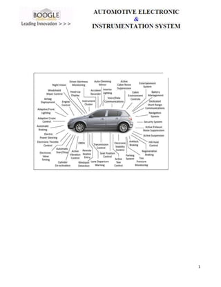
Unit II Sensors and actuators
Speed sensors, Pressure sensors: Manifold Absolute Pressure sensor, knock sensor, Temperature
sensors: Coolant and Exhaust gas temperature, Exhaust Oxygen level sensor, Position sensors:
Throttle position sensor, accelerator pedal position sensor and crankshaft position sensor, Air
mass flow sensor. Solenoids, stepper motors and relays
43. 43
2. Speed Sensor
2.1 Pick-Up Coil (Variable Reluctance) Type Sensors
This type of sensor consists of a permanent magnet, yoke, and coil. This sensor is mounted close to
a toothed gear. As each tooth moves by the sensor, an AC voltage pulse is induced in the coil. Each
tooth produces a pulse. As the gear rotates faster there more pulses are produced. The ECM
determines the speed the component is revolving based on the number of pulses. The number of
pulses in one second is the signal frequency.
The distance between the rotor and pickup coil is critical. The further apart they are, the weaker the
signal.
Not all rotors use teeth. Sometimes the rotor is notched, which will produce the same effect.
These sensors generate AC voltage, and do not need an external power supply. Another common
characteristic is that they have two wires to carry the AC voltage.
The wires are twisted and shielded to prevent electrical interference from disrupting the signal.
The EWD will indicate if the wires are shielded.
By knowing the position of the camshaft, the ECM can determine when cylinder No. I is on the
compression stroke. The ECM uses this information for fuel injection timing, for direct ignition
systems and for variable valve timing systems.
This sensor is located near one of the camshafts. With variable timing V-type engines, there is one
sensor for each cylinder bank. On distributor ignition systems, it is often called the G sensor and is
44. 44
located in the distributor.
An AC signal is generated that is directly proportional to camshaft speed. That is, as the camshaft
revolves faster the frequency increases.
2.2 Pressure sensors:
Pressure sensors are used to measure intake manifold pressure, atmospheric pressure, vapor
pressure in the fuel tank, etc. Though the location is different, and the pressures being measured
vary, the operating principles are similar.
45. 45
2.2.1 Manifold Absolute Pressure (MAP) Sensor
In the Manifold Absolute Pressure (MAP) sensor there is a silicon chip mounted inside a reference
chamber. On one side of the chip is a reference pressure. This reference pressure is either a perfect
vacuum or a calibrated pressure, depending on the application. On the other side is the pressure to
be measured. The silicon chip changes its resistance with the changes in pressure. When the silicon
chip flexes with the change in pressure, the electrical resistance of the chip changes. This change in
resistance alters the voltage signal. The ECM interprets the voltage signal as pressure and any
change in the voltage signal means there was a change in pressure. Intake manifold pressure is a
directly related to engine load. The ECM needs to know intake manifold pressure to calculate how
much fuel to inject, when to ignite the cylinder, and other functions. The MAP sensor is located
either directly on the intake manifold or it is mounted high in the engine compartment and
connected to the intake manifold with vacuum hose. It is critical the vacuum hose not have any
kinks for proper operation.
46. 46
The MAP sensor uses a perfect vacuum as a reference pressure. The difference in pressure between
the vacuum pressure and intake manifold pressure changes the voltage signal. The MAP sensor
converts the intake manifold pressure into a voltage signal (PIM).
47. 47
The MAP sensor voltage signal is highest when intake manifold pressure is highest (ignition key
ON, engine off or when the throttle is suddenly opened). The MAP sensor voltage signal is lowest
when intake manifold pressure is lowest on deceleration with throttle closed.
MAP Sensor Diagnosis
The MAP sensor can cause a variety of driveability problems since it is an important sensor for fuel
injection and ignition timing. Visually check the sensor, connections, and vacuum hose. The
vacuum hose should be free of kinks, leaks, obstructions and connected to the proper port.
The VC (VCQ wire needs to supply approximately 5 volts to the MAP sensor. The E2 ground wire
should not have any resistance. Sensor calibration and performance is checked by applying different
pressures and comparing to the voltage drop specification. The voltage drop is calculated by
subtracting the PIM voltage from the VC voltage.
48. 48
3. Knock Sensor
The Knock Sensor detects engine knock and sends a voltage signal to the ECM. The ECM uses the
Knock Sensor signal to control timing. Engine knock occurs within a specific frequency range. The
Knock Sensor, located in the engine block, cylinder head, or intake manifold is tuned to detect that
frequency.
Inside the knock sensor is a piezoelectric element. Piezoelectric elements generate a voltage when
pressure or a vibration is applied to them. The piezoelectric element in the knock sensor is tuned to
the engine knock frequency.
49. 49
The vibrations from engine knocking vibrate the piezoelectric element generating a voltage. The
voltage output from the Knock Sensor is highest at this time.
4. Temperature Sensors:
The ECM needs to adjust a variety of systems based on temperatures. It is critical for proper
operation of these systems that the engine reach operating temperature and the temperature is
accurately signaled to the ECM. For example, for the proper amount of fuel to be injected the ECM
must know the correct engine temperature. Temperature sensors measure Engine Coolant
Temperature (ECT), Intake Air Temperature (IAT) and Exhaust Recirculation Gases (EGR), etc.
50. 50
4.1 Engine Coolant Temperature (ECT) Sensor
The ECT responds to change in Engine Coolant Temperature. By measuring engine coolant
temperature, the ECM knows the average temperature of the engine. The ECT is usually located in
a coolant passage just before the thermostat. The ECT is connected to the THW terminal on the
ECM.
The ECT sensor is critical to many ECM functions such as fuel injection, ignition timing, variable
valve timing, transmission shifting, etc. Always check to see if the engine is at operating
52. 52
4.2 Exhaust Gas Recirculation (EGR) Temperature Sensor
The EGR Temperature Sensor is located in the EGR passage and measures the temperature of the
exhaust gases. The EGR Temp sensor is connected to the THG terminal on the ECM. When the
EGR valve opens, temperature increases. From the increase in temperature, the ECM knows the
EGR valve is open and that exhaust gases are flowing.
ECT & EGR Temperature Sensor Operation
Though these sensors are measuring different things, they all operate in the same way. From the
voltage signal of the temperature sensor, the ECM knows the temperature. As the temperature of the
sensor heats up, the voltage signal decreases. The decrease in the voltage signal is caused by the
decrease in resistance. The change in resistance causes the voltage signal to drop. The temperature
sensor is connected in series to a fixed value resistor. The ECM supplies 5 volts to the circuit and
measures the change in voltage between the fixed value resistor and the temperature sensor. When
the sensor is cold, the resistance of the sensor is high, and the voltage signal is high. As the sensor
warms up, the resistance drops and voltage signal decreases. From the voltage signal, the ECM can
determine the temperature of the coolant, intake air, or exhaust gas temperature. The ground wire of
the temperature sensors is always at the ECU usually terminal E2. These sensors are classified as
thermistors.
Temperature Sensor Diagnostics
Temperature sensor circuits are tested for:
• opens.
• Shorts.
• Available voltage.
• Sensor resistance.
The Diagnostic Tester data list can reveal the type of problem. An open circuit (high resistance) will
read the coldest temperature possible. A shorted circuit (low resistance) will read the highest
temperature possible. The diagnostic procedure purpose is to isolate and identify the temperature
sensor from the circuit and ECM.
High resistance in the temperature circuit will cause the ECM to think that the temperature is colder
than it really is. For example, as the engine warms up, ECT resistance decreases, but unwanted
extra resistance in the circuit will produce a higher voltage drop signal. This will most likely be
53. 53
noticed when the engine has reached operating temperatures. Note that at the upper end of the
temperature/resistance scale, ECT resistance changes very little. Extra resistance in the higher
temperature can cause the ECM to think the engine is approximately 20'F = 30'F colder than actual
temperature. This will cause poor engine performance, fuel economy, and possibly engine
overheating.
Solving Open Circuit Problems
A jumper wire and Diagnostic Tester are used to locate the problem in an open circuit.
54. 54
Solving Shorted Circuit Problems
Creating an open circuit at different points in the temperature circuit will isolate the short. The
temperature reading should go extremely low (cold) when an open is created.
4.3 Oxygen and Air/Fuel Ratio Sensors
The ECM uses an oxygen sensor to ensure the air/fuel ratio is correct for the catalytic converter.
55. 55
Based on the oxygen sensor signal, the ECM will adjust the amount of fuel injected into the intake
air stream. There are different types of oxygen sensors, but two of the more common types are:
• The narrow range oxygen sensor, the oldest style, simply called the oxygen sensor.
• Wide range oxygen sensor, the newest style, called the air/fuel ratio (A/F) sensor.
Also used on very limited models in the early 90s, was the Titania oxygen sensor.
OBD II vehicles require two oxygen sensors: one before and one after the catalytic converter. The
oxygen sensor, or air/fuel ratio sensor, before the catalytic converter is used by the ECM to adjust
the air/fuel ratio. This sensor in OBD II terms is referred to as sensor 1. On V-type engines one
sensor will be referred to as Bank I Sensor 1 and the other as Bank 2 Sensor 1. The oxygen sensor
after the catalytic converter is used by the ECM primarily to determine catalytic converter
efficiency. This sensor is refer-red to as sensor 2. With two catalytic converters, one sensor will be
Bank 1 Sensor 2 and the other as Bank 2 Sensor 2.
Titania Element Type Oxygen Sensor
This oxygen sensor consists of a semiconductor element made of titanium dioxide (TiO2, which is,
like ZrO2, a kind of ceramic). This sensor uses a thick film type titania element formed on the front
end of a laminated substrate to detect the oxygen concentration in the exhaust gas.
56. 56
Operation
The properties of titania are such that its resistance changes in accordance with the oxygen
concentration of the exhaust gas. This resistance changes abruptly at the boundary between a lean
and a rich theoretical air/fuel ratio, as shown in the graph. The resistance of titania also changes
greatly in response to changes in temperature. A heater is, thus built into the laminated substrate to
keep the temperature of the element constant.
This sensor is connected to the ECM as shown in the following circuit diagram. A 1.0 volt potential
is supplied at all times to the 0" positive (+) terminal by the ECM. The ECM has a builtin
57. 57
comparator that compares the voltage drop at the Ox terminal (due to the change in resistance of the
titania) to a reference voltage (0.45 volts). If the result shows that the Ox voltage is greater than
0.45 volts (that is, if the oxygen sensor resistance is low), the ECM judges that the air/fuel ratio is
rich. If the 0, voltage is lower than 0.45 volts (oxygen sensor resistance high), it judges that the
air/fuel ratio is lean.
Oxygen Sensor
This style of oxygen sensor has been in service the longest time. It is made of zirconia (zirconium
dioxide), platinum electrodes, and a heater. The oxygen sensor generates a voltage signal based on
the amount of oxygen in the exhaust compared to the atmospheric oxygen. The zirconia element has
one side exposed to the exhaust stream, the other side open to the atmosphere. Each side has a
platinum electrode attached to Zirconium dioxide element. The platinum electrodes conduct the
voltage generated. Contamination or corrosion of the platinum electrodes or zirconia elements will
reduce the voltage signal output.
58. 58
Operation
When exhaust oxygen content is high, oxygen sensor voltage output is low. When exhaust oxygen
content is low, oxygen sensor voltage output is high. The greater the difference in oxygen content
between the exhaust stream and atmosphere, the higher the voltage signal.
From the oxygen content, the ECM can determine if the air/fuel ratio is rich or lean and adjusts the
fuel mixture accordingly. A rich mixture consumes nearly all the oxygen, so the voltage signal is
high, in the range of 0.6 - 1.0 volts. A lean mixture has more available oxygen after combustion
than a rich mixture, so the voltage signal is low, 0.4 - 0.1 volts. At the stoichiometric air/fuel ratio
(14.7: 1), oxygen sensor voltage output is approximately 0.45 volts.
59. 59
Small changes in the air/fuel ratio from the stoichiometric point radically changes the voltage
signal. This type of oxygen sensor is sometimes referred to as a narrow range sensor because it
cannot detect the small changes in the exhaust stream oxygen content produced by changes in the
air/fuel mixture. The ECM will continuously add and subtract fuel producing a rich/lean cycle.
Refer to Closed Loop Fuel Control in the Fuel Injection section for more information.
NOTE: Think of the oxygen sensor as a switch. Each time the air/fuel ratio is at stoichiometry
(14.7: 1) the oxygen sensor switches either high or low.
60. 60
The oxygen sensor will only generate an accurate signal when it has reached a minimum operating
temperature of 400'C (7500F). To quickly warm up the oxygen sensor and to keep it hot at idle and
light load conditions, the oxygen sensor has a heater built into it. This heater is controlled by the
ECM. See Oxygen Sensor Heater Control for more information.
Operation
A detection circuit in the ECM detects the change and strength of current flow and puts out a
voltage signal relatively proportional to exhaust oxygen content.
NOTE: This voltage signal can only be measured by using the Diagnostic Tester or OBD II
compatible scan tool. The A/F sensor current output cannot be accurately measured directly. If an
OBD 11 scan tool is used, refer to the Repair Manual for conversion, for the output signal is
different.
The A/F sensor is designed so that at stoichiometry, there is no current flow and the voltage put out
by the detection circuit is 3.3 volts. A rich mixture, which leaves very little oxygen in the exhaust
stream, produces a negative current flow. The detection circuit will produce a voltage below 3.3
volts. A lean mixture, which has more oxygen in the exhaust stream, produces a positive current
flow. The detection circuit will now produce a voltage signal above 3.3 volts.
62. 62
Oxygen Sensor Diagnosis Service
There are several factors that can affect the normal functioning of the oxygen sensor. It is important
to isolate if it is the oxygen sensor itself or some other factor causing the oxygen sensor to behave
abnormally. See Course 874 Technician Reference book for more information. A contaminated
oxygen sensor, will not produce the proper voltages and will not switch properly. The sensor can be
contaminated from engine coolant, excessive oil consumption, additives used in sealants, and the
wrong additives in gasoline. When lightly contaminated, the sensor is said to be "lazy," because of
the longer time it takes to switch from rich to lean and/or vice versa. This will adversely affect
emissions and can produce driveability problems. Many factors can affect the operation of the
oxygen sensor, such as a vacuum leak, an EGR leak, excessive fuel pressure, etc.
It is also very important that the oxygen sensor and heater electrical circuits be in excellent
condition. Excessive resistance, opens, and shorts to ground will produce false voltage signals. In
many cases, DTCs or basic checks will help locate the problem.
5. Position Sensors
In many applications, the ECM needs to know the position of mechanical components. The Throttle
Position Sensor (TPS) indicates position of the throttle valve. Accelerator Pedal Position (APP)
sensor indicates position of the accelerator pedal. Exhaust Gas Valve (EGR) Valve Position Sensor
indicates position of the EGR Valve. The vane air flow meter uses this principle. Electrically, these
sensors operate the same way. A wiper arm inside the sensor is mechanically connected to a moving
part, such as a valve or vane. As the part moves, the wiper arm also moves. The wiper arm is also in
contact with a resistor. As the wiper arm moves on the resistor, the signal voltage output changes.
At the point of contact the available voltage is the signal voltage and this indicates position. The
closer the wiper arm gets to VC voltage, the higher the signal voltage output. From this voltage, the
ECM is able to determine the position of a component.
63. 63
5.1 Throttle Position Sensor
The TPS is mounted on the throttle body and converts the throttle valve angle into an electrical
signal. As the throttle opens, the signal voltage increases.
The ECM uses throttle valve position information to know:
• engine mode: idle, part throttle, wide open throttle.
64. 64
• switch off AC and emission controls at Wide Open Throttle (WOT).
• air-fuel ratio correction.
• power increase correction.
• fuel cut control.
The basic TPS requires three wires. Five volts are supplied to the TPS from the VC terminal of the
ECM. The TPS voltage signal is supplied to the VTA terminal. A ground wire from the TPS to the
E2 terminal of the ECM completes the circuit.
At idle, voltage is approximately 0.6 - 0.9 volts on the signal wire. From this voltage, the ECM
knows the throttle plate is closed. At wide open throttle, signal voltage is approximately 3.5 - 4.7
volts. Inside the TPS is a resistor and a wiper arm. The arm is always contacting the resistor. At the
point of contact, the available voltage is the signal voltage and this indicates throttle valve position.
At idle, the resistance between the VC (or VCC terminal and VTA terminal is high, therefore, the
available voltage is approximately 0.6 - 0.9 volts. As the contact arm moves closer the VC terminal
(the 5 volt power voltage), resistance decreases and the voltage signal increases.
65. 65
Some TPS incorporate a Closed Throttle Position switch (also called an idle contact switch). This
switch is closed when the throttle valve is closed. At this point, the ECM measures 0 volts and there
is 0 volts at the IDL terminal. When the throttle is opened, the switch opens and the ECM reads +B
voltage at the IDL circuit.
66. 66
The TPS on the ETCS-i system has two contact arms and to resistors in one housing. The first
signal line is VTA1 and the second signal line is VTA2.
VTA2 works the same, but starts at a higher voltage output and the voltage change rate is different
from VTA1 As the throttle opens the two voltage signals increase at a different rate. The ECM uses
both signals to detect the change in throttle valve position. By having two sensors, ECM can
compare the voltages and detect problems.
5.2 Accelerator Pedal Position (APP) Sensor
The APP sensor is mounted on the throttle body of the ETCS-i. The APP sensor converts the
accelerator pedal movement and position into two electrical signals. Electrically, the APP is
identical in operation to the TPS.
67. 67
EGR Valve Position Sensor
The EGR Valve Position Sensor is mounted on the EGR valve and detects the height of the EGR
valve. The ECM uses this signal to control EGR valve height. The EGR Valve Position Sensor
converts the movement and position of the EGR valve into an electrical signal. Operation is
identical to the TPS except that the signal arm is moved by the EGR valve.
5.3 Crankshaft Position Sensor (NE Sensor)
The ECM uses crankshaft position signal to determine engine RPM, crankshaft position, and engine
misfire. This signal is referred to as the NE signal. The NE signal combined with the G signal
indicates the cylinder that is on compression and the ECM can determine from its programming the
engine firing order. See Section 3 on ignition systems for more information.
69. 69
6. Air/Fuel Ratio Sensor
The Air/Fuel Ratio (A/F) sensor is similar to the narrow range oxygen sensor. Though it appears
similar to the oxygen sensor, it is constructed differently and has different operating characteristics.
The A/F sensor is also referred to as a wide range or wide ratio sensor because of its ability to detect
air/fuel ratios over a wide range.
The advantage of using the A/F sensor is that the ECM can more accurately meter the fuel reducing
emissions. To accomplish this, the A/F sensor:
• operates at approximately 650'C (1200'F), much hotter than the oxygen sensor 400'C
(750'F).
• changes its current (amperage) output in relation to the amount of oxygen in the exhaust stream.
70. 70
Operation
A detection circuit in the ECM detects the change and strength of current flow and puts out a
bvoltage signal relatively proportional to exhaust oxygen content.
NOTE: This voltage signal can only be measured by using the Diagnostic Tester or OBD II
compatible scan tool. The A/F sensor current output cannot be accurately measured directly. If an
OBD 11 scan tool is used, refer to the Repair Manual for conversion, for the output signal is
different. The A/F sensor is designed so that at stoichiometry, there is no current flow and the
voltage put out by the detection circuit is 3.3 volts. A rich mixture, which leaves very little oxygen
in the exhaust stream, produces a negative current flow. The detection circuit will produce a voltage
below 3.3 volts. A lean mixture, which has more oxygen in the exhaust stream, produces a positive
current flow. The detection circuit will now produce a voltage signal above 3.3 volts.
NOTE
The A/F sensor voltage output is the opposite of what happens in the narrow range oxygen sensor.
71. 71
Voltage output through the detection circuit increases as the mixture gets leaner. Also, the voltage
signal is proportional to the change in the air/fuel mixture. This allows the ECM to more accurately
judge the exact air/fuel ratio under a wide variety of conditions and quickly adjust the amount of
fuel to the stoichiometric point. This type of rapid correction is not possible with the narrow range
oxygen sensor. With an A/F sensor, the ECM does not follow a rich lean cycle. Refer to Closed
Loop Fuel Control in the Fuel Injection chapter for more information.
HINT
Think of the A/F sensor as a generator capable of changing polarity. When the fuel mixture is rich
(high exhaust oxygen content), the A/F generates current in the negative (-) direction. As the
air/fuel mixture gets leaner (less oxygen content), the A/F sensor generates current in the positive
(+) direction. At the stoichiometric point, no current is generated. The detection circuit is always
measuring the direction and how much current is being produced. The result is that the ECM knows
exactly how rich or lean the mixture is and can adjust the fuel mixture much faster than the oxygen
sensor based fuel control system. Therefore, there is no cycling that is normal for a narrow range
oxygen sensor system. Instead, A/F sensor output is more even and usually around 3.3 volts.
7. Solenoids:
A solenoid is a coil of insulated or enameled wire wound on a rod-shaped form made of solid iron,
solid steel, or powdered iron. Devices of this kind can be used as electromagnets, as inductors in
electronic circuits, and as miniature wireless receiving antennas. In a solenoid, the core material is
ferromagnetic, meaning that it concentrates magnetic lines of flux. This increases the inductance of
the coil far beyond the inductance obtainable with an air-core coil of the same dimensions and the
same number of turns. When current flows in the coil, most of the resulting magnetic flux exists
within the core material. Some flux appears outside the coil near the ends of the core; a small
amount of flux also appears outside the coil and off to the side. A solenoid chime is wound on a
cylindrical, hollow, plastic or phenolic form with a movable, solid iron or steel core. The core can
travel in and out of the coil along its axis. The coil is oriented vertically; the core normally rests
somewhat below the coil center. When a current pulse is applied to the coil, the magnetic field pulls
the core forcefully upward. Inertia carries the core above the center of the coil, where the core
72. 72
strikes a piece of metal similar to a xylophone bell, causing a loud "ding".
How Solenoids Work
Inside a solenoid is motor wire coiled in a special way (see image above). When send an electric
current through this wire (energized), a magnetic field is created. The inner shaft of a solenoid is a
piston like cylinder made of iron or steel, called the plunger or slug (equivalent to an armature). The
magnetic field then applies a force to this plunger, either attracting or repeling it. When the
magnetic field is turned off, a spring then returns the plunger to its original state.
Push and Pull Type Solenoids
There are two main types of solenoids. The type directly refers to the solenoid start and energized
positions, and is very important to understand. In pull type solenoids (image above), the plunger is
normally outside the solenoid because the spring naturally forces the plunger out. Yet when
energized, the force 'pulls' the plunger into the solenoid. Push type solenoids are the opposite, in