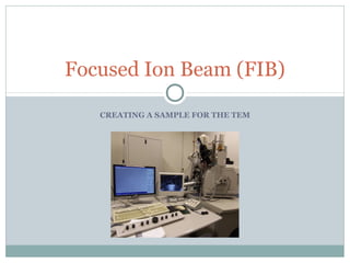
SlideShare a Scribd company logo
1 of 12
CREATING A SAMPLE FOR THE TEM
Focused Ion Beam (FIB)
How it works?
Reasons for one electron beam
and one ion beam
 Viewing three dimensions
 SEM provides view of x- and y-directions
 FIB provides view of y- and z-directions
 Monitoring sample fabrication with non-
destructive SEM
 Determining if the final sample is of uniform
thickness
 Brightness of sample should be consistent
How it works?
Eucentric height adjustments
 Sample holder is tilted back and forth
 Height (z-direction) is adjusted until the area of interest
remains centered at all tilts
 Both FIB and SEM can view the same area
Eucentric height is
typically around 5mm in
most FIBs
How it works?
Sample protection (Pt deposition)
 Wetting of tungsten tip to make Ga+
ions
 Injection of Pt-based metallorganic gas
 Pt is deposited and organics leave
 Pt coating protects the area of interest
from further ion damage
How it works?
Ion milling
 Trenches are created around the area of interest
 Milling is monitored by the SEM beam
Sample cutting
 Rectangular sample is cut so
that it is barely attached
Pt
How it works?
View of milled sample
How it works?
Sample Plucking
 Pt gas probe reinserted
 Sample plucker is inserted
 Plucker is microwelded to the
sample
 TEM sample is lifted from the bulk
material
How it works?
Welding to the TEM grid
 Eucentric height of grid is found
 Sample is moved against the grid
 Sample is microwelded to the grid
 Plucker is ion milled off
How it works?
View of mounted sample
How it works?
Sample polishing
 Needed for atomic resolution in TEM
 Eliminates ion impurities from milling (surface damage)
 Low current is used to prevent impurities and surface damage
 Final sample is ~100nm thick
 Final sample must have parallel surfaces and consistent
thickness
 Final sample will be bright due to electron transparency
What we are looking for
Grain boundary complexions
What we are looking for
A good high resolution TEM image of complexions

More Related Content

What's hot

Chemical vapour deposition
Chemical vapour depositionChemical vapour deposition
Chemical vapour deposition
Sethu Ram
 
03 magnesium and magnesium alloys
03 magnesium and magnesium alloys03 magnesium and magnesium alloys
03 magnesium and magnesium alloys
cha3068
 
Ceramic matrix composite
Ceramic matrix compositeCeramic matrix composite
Ceramic matrix composite
Gulfam Hussain
 
Auger electron spectroscopy
Auger electron spectroscopyAuger electron spectroscopy
Auger electron spectroscopy
Gulfam Hussain
 

What's hot (20)

Physical vapor deposition
Physical vapor depositionPhysical vapor deposition
Physical vapor deposition
 
Lithography and Nanolithography
Lithography and NanolithographyLithography and Nanolithography
Lithography and Nanolithography
 
Chemical vapour deposition
Chemical vapour depositionChemical vapour deposition
Chemical vapour deposition
 
Electrochemical Characterization of Electrocatalysts .pptx
Electrochemical Characterization of Electrocatalysts .pptxElectrochemical Characterization of Electrocatalysts .pptx
Electrochemical Characterization of Electrocatalysts .pptx
 
Maraging steel
Maraging steelMaraging steel
Maraging steel
 
Grain size measurement according to astm standards
Grain size measurement according to astm standardsGrain size measurement according to astm standards
Grain size measurement according to astm standards
 
SEM,TEM & AFM
SEM,TEM & AFMSEM,TEM & AFM
SEM,TEM & AFM
 
Metal matrix composites (mmc)
Metal matrix composites (mmc)Metal matrix composites (mmc)
Metal matrix composites (mmc)
 
Ion beam etching (or) Ion milling
Ion beam etching (or) Ion millingIon beam etching (or) Ion milling
Ion beam etching (or) Ion milling
 
Nano Indentation Lecture1
Nano Indentation Lecture1Nano Indentation Lecture1
Nano Indentation Lecture1
 
03 magnesium and magnesium alloys
03 magnesium and magnesium alloys03 magnesium and magnesium alloys
03 magnesium and magnesium alloys
 
Ceramic matrix composite
Ceramic matrix compositeCeramic matrix composite
Ceramic matrix composite
 
X ray photoelectron spectroscopy
X ray photoelectron spectroscopyX ray photoelectron spectroscopy
X ray photoelectron spectroscopy
 
STM ppt
STM pptSTM ppt
STM ppt
 
Metal matrix Composites
Metal matrix CompositesMetal matrix Composites
Metal matrix Composites
 
X ray photoelectron spectroscopy (xps)
X ray photoelectron spectroscopy (xps)X ray photoelectron spectroscopy (xps)
X ray photoelectron spectroscopy (xps)
 
Metallography and microscopy
Metallography and microscopyMetallography and microscopy
Metallography and microscopy
 
AFM (Atomic Force Microscopy)
AFM (Atomic Force Microscopy)AFM (Atomic Force Microscopy)
AFM (Atomic Force Microscopy)
 
Auger electron spectroscopy
Auger electron spectroscopyAuger electron spectroscopy
Auger electron spectroscopy
 
Electrodeposited Ni- Based nano composites
Electrodeposited Ni- Based nano compositesElectrodeposited Ni- Based nano composites
Electrodeposited Ni- Based nano composites
 

Similar to FIB Presentation

Types of electron microscope
Types of electron microscopeTypes of electron microscope
Types of electron microscope
Asad Leo
 

Similar to FIB Presentation (20)

Tunneling electron Microscopy, Scanning electron microscopy
Tunneling electron Microscopy, Scanning electron microscopyTunneling electron Microscopy, Scanning electron microscopy
Tunneling electron Microscopy, Scanning electron microscopy
 
Scanning Electron Microscopy
Scanning Electron MicroscopyScanning Electron Microscopy
Scanning Electron Microscopy
 
Stm 07.08.13
Stm 07.08.13Stm 07.08.13
Stm 07.08.13
 
Specimenprep
SpecimenprepSpecimenprep
Specimenprep
 
Scaning electron microscop
Scaning electron microscopScaning electron microscop
Scaning electron microscop
 
Scanning electron microscope
Scanning electron microscopeScanning electron microscope
Scanning electron microscope
 
Characterization of materials lec 17
Characterization of materials  lec 17Characterization of materials  lec 17
Characterization of materials lec 17
 
Microscopic Analysis of Ceramic Materials.pptx
Microscopic Analysis of Ceramic Materials.pptxMicroscopic Analysis of Ceramic Materials.pptx
Microscopic Analysis of Ceramic Materials.pptx
 
Scanning Tunnelling Microscope (STM).pdf
Scanning Tunnelling Microscope (STM).pdfScanning Tunnelling Microscope (STM).pdf
Scanning Tunnelling Microscope (STM).pdf
 
Scanning electon microscope. Dr. GAURAV SALUNKHE
Scanning electon microscope. Dr. GAURAV SALUNKHEScanning electon microscope. Dr. GAURAV SALUNKHE
Scanning electon microscope. Dr. GAURAV SALUNKHE
 
Atomic Force Microscope: Fundamental Principles
Atomic Force Microscope: Fundamental PrinciplesAtomic Force Microscope: Fundamental Principles
Atomic Force Microscope: Fundamental Principles
 
Lecture-4 SEM.pptx
Lecture-4 SEM.pptxLecture-4 SEM.pptx
Lecture-4 SEM.pptx
 
Lecture-4 SEM.ppt
Lecture-4 SEM.pptLecture-4 SEM.ppt
Lecture-4 SEM.ppt
 
Lecture-4 SEM.ppt
Lecture-4 SEM.pptLecture-4 SEM.ppt
Lecture-4 SEM.ppt
 
Types of electron microscope
Types of electron microscopeTypes of electron microscope
Types of electron microscope
 
ATOMIC FORCE MICROSCOPY.ppt
ATOMIC FORCE MICROSCOPY.pptATOMIC FORCE MICROSCOPY.ppt
ATOMIC FORCE MICROSCOPY.ppt
 
BMNS
BMNS BMNS
BMNS
 
Electron microscope
Electron microscopeElectron microscope
Electron microscope
 
7 nanotools_spm.pdf
7 nanotools_spm.pdf7 nanotools_spm.pdf
7 nanotools_spm.pdf
 
Scanning electron microscope
Scanning electron microscope  Scanning electron microscope
Scanning electron microscope
 

More from George Ferko (11)

5 Levels of Leadership for New Sales Mangers
5 Levels of Leadership for New Sales Mangers5 Levels of Leadership for New Sales Mangers
5 Levels of Leadership for New Sales Mangers
 
Netflix Presentation - George's
Netflix Presentation - George'sNetflix Presentation - George's
Netflix Presentation - George's
 
Spinel-Yb grain growth and prob analysis
Spinel-Yb grain growth and prob analysisSpinel-Yb grain growth and prob analysis
Spinel-Yb grain growth and prob analysis
 
Doped Titania Project Zinc Focus - George J. Ferko V
Doped Titania Project Zinc Focus - George J. Ferko VDoped Titania Project Zinc Focus - George J. Ferko V
Doped Titania Project Zinc Focus - George J. Ferko V
 
IPD Final Presentation-2
IPD Final Presentation-2IPD Final Presentation-2
IPD Final Presentation-2
 
APT Presentation - George J. Ferko V
APT Presentation - George J. Ferko VAPT Presentation - George J. Ferko V
APT Presentation - George J. Ferko V
 
27-750 Spinel Final Notes
27-750 Spinel Final Notes27-750 Spinel Final Notes
27-750 Spinel Final Notes
 
MST'11 Spinel Finalish
MST'11 Spinel FinalishMST'11 Spinel Finalish
MST'11 Spinel Finalish
 
Luo Presentation
Luo PresentationLuo Presentation
Luo Presentation
 
Summer Spinel Research - Ferko - 2009
Summer Spinel Research - Ferko - 2009Summer Spinel Research - Ferko - 2009
Summer Spinel Research - Ferko - 2009
 
The Junctionless Transistor - George J. Ferko V
The Junctionless Transistor - George J. Ferko VThe Junctionless Transistor - George J. Ferko V
The Junctionless Transistor - George J. Ferko V
 

FIB Presentation

  • 1. CREATING A SAMPLE FOR THE TEM Focused Ion Beam (FIB)
  • 2. How it works? Reasons for one electron beam and one ion beam  Viewing three dimensions  SEM provides view of x- and y-directions  FIB provides view of y- and z-directions  Monitoring sample fabrication with non- destructive SEM  Determining if the final sample is of uniform thickness  Brightness of sample should be consistent
  • 3. How it works? Eucentric height adjustments  Sample holder is tilted back and forth  Height (z-direction) is adjusted until the area of interest remains centered at all tilts  Both FIB and SEM can view the same area Eucentric height is typically around 5mm in most FIBs
  • 4. How it works? Sample protection (Pt deposition)  Wetting of tungsten tip to make Ga+ ions  Injection of Pt-based metallorganic gas  Pt is deposited and organics leave  Pt coating protects the area of interest from further ion damage
  • 5. How it works? Ion milling  Trenches are created around the area of interest  Milling is monitored by the SEM beam Sample cutting  Rectangular sample is cut so that it is barely attached Pt
  • 6. How it works? View of milled sample
  • 7. How it works? Sample Plucking  Pt gas probe reinserted  Sample plucker is inserted  Plucker is microwelded to the sample  TEM sample is lifted from the bulk material
  • 8. How it works? Welding to the TEM grid  Eucentric height of grid is found  Sample is moved against the grid  Sample is microwelded to the grid  Plucker is ion milled off
  • 9. How it works? View of mounted sample
  • 10. How it works? Sample polishing  Needed for atomic resolution in TEM  Eliminates ion impurities from milling (surface damage)  Low current is used to prevent impurities and surface damage  Final sample is ~100nm thick  Final sample must have parallel surfaces and consistent thickness  Final sample will be bright due to electron transparency
  • 11. What we are looking for Grain boundary complexions
  • 12. What we are looking for A good high resolution TEM image of complexions