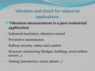
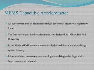
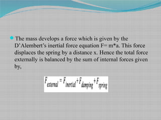
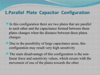
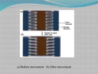
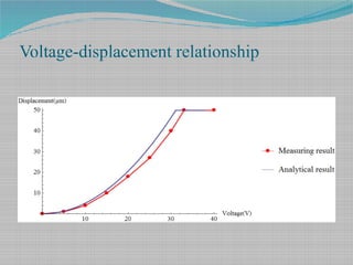
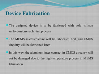
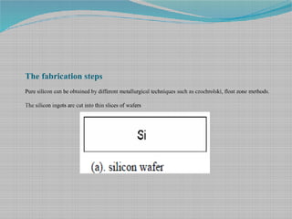
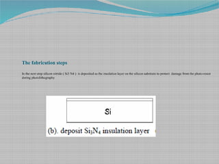
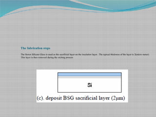
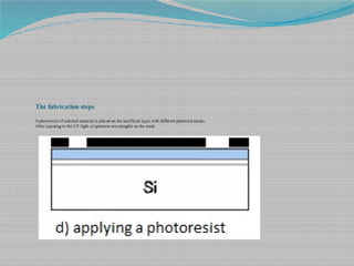
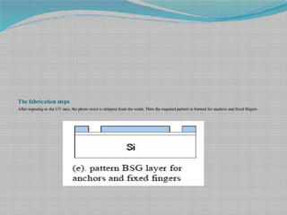
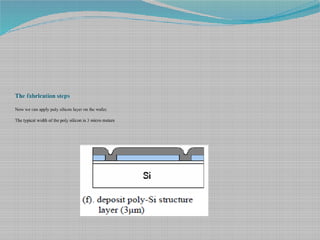
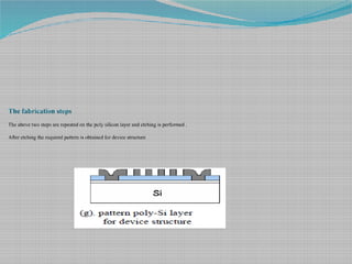
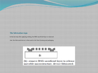
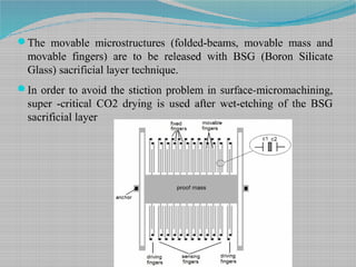
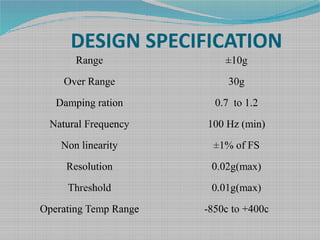
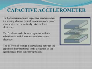
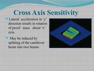
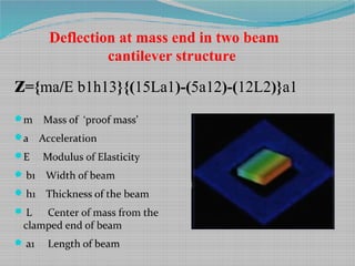
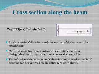
MEMS CAPACITIVE
ACCELEROMETER
Introduction
What is MEMS Technology?
MEMS technology is based on a number of tools and
methodologies, which are used to form small structures with
dimensions in the micrometer scale
MEMS fabrication approach that conveys the advantages of
miniaturization, multiple components, and microelectronics to
the design and construction of integrated Electromechanical
systems
What are MEMS and Size?
MEMS
• Micro - Small size, microfabricated structures
• Electro - Electrical signal /control ( In / Out )
• Mechanical - Mechanical functionality (Out/ In )
• Systems - Structures, Devices, Systems controls
Size
They range in size from the sub micron level to the
millimeter level, and there can be any number, from a few
to millions, in a particular system.
Materials for MEMS
 Silicon
 Germanium
 Gallium Arsenide
 Quartz
 Plastics and Polymers
 Ceramics
 Metals
MEMS Capacitive Accelerometer
 An accelerometer is an electromechanical device that measures acceleration
forces
 The first micro machined accelerometer was designed in 1979 at Stanford
University.
 In the 1990s MEMS accelerometers revolutionized the automotive-airbag
system industry.
 Micro machined accelerometers are a highly enabling technology with a
huge commercial potential.
MEMS Capacitive Accelerometer
 They provide lower power, compact and robust sensing. Multiple sensors
are often combined to provide multi-axis sensing and more accurate data .
 An accelerometer is a device that measures the vibration, or acceleration
of motion of a structure. The force caused by vibration or a change in
motion (acceleration) causes the mass to "squeeze" the piezoelectric
material which produces an electrical charge that is proportional to the
force exerted upon it.
Working accelerometer
PRINCIPLE OPERATION
An accelerometer generally consists of a proof mass suspended
by compliant beams anchored to a fixed frame. The proof mass
has a mass of m, the suspension beams have an effective spring
constant stiffness k and there is a damping factor (b) affecting
the dynamic movement of the mass generated by the air-
structure interaction. The accelerometer can be modeled by a
second-order Mass-damper-spring system,
GENERAL WORKING PRINCIPLE
External acceleration displaces the support frame relative
to the proof mass, which in turn changes the internal stress
in the suspension spring. Both this relative displacement
and the suspension-beam stress can be used as a measure
of the external acceleration.
The mass develops a force which is given by the
D’Alembert’s inertial force equation F= m*a. This force
displaces the spring by a distance x. Hence the total force
externally is balanced by the sum of internal forces given
by,
Basic Mechanics
Stress is the defined as the force per unit area acting on
the surface of a differential volume element of a solid
body.
The strain, which can be defined as the deformation
resulting from a stress.
Spring Constant
 Spring Constant (proportionality constant) that relates the
force and the displacement in Hooke’s law.
By increasing or decreasing the spring constant we can alter
the movement of the proof mass in the corresponding
direction
Capacitance Basics
MEMS capacitance configurations can be characterized into
three parts
Parallel Plate Capacitor Configuration
Transverse Comb Capacitance Configuration
Lateral Comb Capacitance Configuration
1.Parallel Plate Capacitor Configuration
In this configuration there are two plates that are parallel
to each other and the capacitance formed between these
plates changes when the distance between these plates
changes
Due to the possibility of large capacitance areas, this
configuration may result very high sensitivity
The main disadvantage of this configuration is the non-
linear force and sensitivity values, which occurs with the
movement of one of the plates towards the other
The voltage difference applied to the electrodes that causes pull-in
is called pull-in voltage
2.Transverse Comb Capacitance Configuration
There is a movable electrode between two stationary
electrodes.
Due to this differential topology, this configuration shows an
almost linear force -displacement and voltage-displacement
relationship
The nonlinearity comes from fringing field capacitances and
this effect is reduced if high aspect ratio fingers are used.
The general connection is to apply 0 and V0 to fixed electrodes
and to applyV0 /2 to the mid-electrode
The force occurs when the mid-electrode is not in the mid-point
of two stationary electrodes.
The difference in electrostatic force so that the electrostatic force
are unequal, there is an initial unequal difference between the
electrodes
a) Before movement b) After movement
3.Lateral Comb Configuration
The capacitance forms between two combs looking each other.
The change of the capacitance is formed by the change of the
distance of these combs.
This configuration shows a constant force-displacement
characteristic, hence does not form an electrostatic spring
constant, but has a very poor sensitivity due to varying overlap
area topology.
Due to this linearity and poor sensitivity this configuration is generally used
in the actuating parts of the sensors
a) Before movement b) After movement
Force displacement relationship
Voltage-displacement relationship
Device Fabrication
The designed device is to be fabricated with poly -silicon
surface-micromachining process
The MEMS microstructure will be fabricated first, and CMOS
circuitry will be fabricated later.
In this way, the aluminum inter connect in CMOS circuitry will
not be damaged due to the high-temperature process in MEMS
fabrication.
The fabrication steps
Pure silicon can be obtained by different metallurgical techniques such as czochrolski, float zone methods.
The silicon ingots are cut into thin slices of wafers
The fabrication steps
In the next step silicon nitride ( Si3 N4 ) is deposited as the insulation layer on the silicon substrate to protect damage from the photo-resist
during photolithography
The fabrication steps
The Boron Silicate Glass is used as the sacrificial layer on the insulation layer . The typical thickness of the layer is 2(micro meter)
This layer is then removed during the etching process
The fabrication steps
A photoresist of selected material is placed on the sacrificial layer with different patterned masks.
After exposing to the UV light of optimum wavelengths on the mask
The fabrication steps
After exposing to the UV rays, the photo resist is stripped from the wafer. Then the required pattern is formed for anchors and fixed fingers
The fabrication steps
Now we can apply poly silicon layer on the wafer.
The typical width of the poly silicon is 3 micro meters
The fabrication steps
The above two steps are repeated on the poly silicon layer and etching is performed .
After etching the required pattern is obtained for device structure
The fabrication steps
In the last step after applying etching, the BSG sacrificial layer is removed.
And the fabricated device is then send to the final cleaning and packaging.
The movable microstructures (folded-beams, movable mass and
movable fingers) are to be released with BSG (Boron Silicate
Glass) sacrificial layer technique.
In order to avoid the stiction problem in surface-micromachining,
super -critical CO2 drying is used after wet-etching of the BSG
sacrificial layer
DESIGN SPECIFICATION
Range ±10g
Over Range 30g
Damping ration 0.7 to 1.2
Natural Frequency 100 Hz (min)
Non linearity ±1% of FS
Resolution 0.02g(max)
Threshold 0.01g(max)
Operating Temp Range -850c to +400c
CAPACTIVE ACCELEROMETER
In bulk micromachined capacitive accelerometers
the sensing element typically comprises of a proof
mass which can move freely between fixed
electrodes.
The fixed electrode forms a capacitor with the
seismic mass which acts as a common centre
electrode.
The differential change in capacitance between the
capacitors is proportional to the deflection of the
seismic mass from the centre position.
PERFORMANCE OF CAPACITIVE
ACCELOROMETER
Advantages:
 Very low sensitivity to temperature drift
 Higher output levels
 Can be readily used in force-balancing
 High linearity.
Challenges:
 Electronics for the signal processing are more complex.
 Sensitive to parasitic capacitances and electromagnetic interference.
Cantilever structure Bridge Structure
Where
 m Mass of ‘proof mass’
 a Acceleration
 E Modulus of Elasticity
 b1 Width of beam
 h1 Thickness of the beam
 L Center of mass from the clamped end of beam
 a1 Length of beam
Deflection of Mass End in single Beam
Cantilever Structure
z={2ma/E b1h13}{(15La1)-(5a12)-(12L2)}a1
Cross Axis Sensitivity
Lateral acceleration in ‘y’
direction results in rotation
of proof mass about ‘x’
axis.
 May be reduced by
splitting of the cantilever
beam into two beams
Deflection at mass end in two beam
cantilever structure
m Mass of ‘proof mass’
a Acceleration
E Modulus of Elasticity
b1 Width of beam
h1 Thickness of the beam
L Center of mass from the
clamped end of beam
a1 Length of beam
z={ma/E b1h13}{(15La1)-(5a12)-(12L2)}a1
Cross section along the beam
Acceleration in ‘x’ direction results in bending of the beam and the
mass lifts up
Motion of mass due to acceleration in ‘x’ direction cannot be
distinguished from mass motion due to normal acceleration
The deflection of the mass in the ‘z’ direction due to acceleration in ‘x’
direction can be expressed mathematically as given above.
Z= {1/2E1}ma(h2-h1)a1(a2-a1/2)
Capacitive variation
 C1 is the capacitance formed between the upper electrode
and the mass.C2 is the capacitance between the lower
electrode and the mass
 C1=C2=C3 when the mass is at rest
 With acceleration movement of the mass is like a fan and
the capacitance between the fixed electrode and movable
electrode can be found out by integration along the length
of the mass.
C1= ∫ εb2/(d0-A-B(x-a1)) dx C2=∫ εb2/(d0+A+B(x-a1)) dx​
• The net change in capacitance can be found by finding C1-C2 and can be
expressed as
ΔC=C1-C2=C0(2A+(a2–a1)B)/d0[1+a2/d02]
The above equation has a linear and non linear part
Damping Analysis
The basic mechanism for micro mechanical
structures is squeeze film air damping.
Damping coefficient for a square mass can be
expressed in terms of the device dimensions in the
following form
Damping coefficient (c)=2[0.42µa24
/d03 ]
Natural Frequency and Damping Coefficient
d0=10
Beam
h1=90 , b1=240 , a1=600
Mass
h2=575, b2=4000, a2-a1=4000
Coventorware Analytical
Natural Frequency 842 Hz 854 Hz
Damping Coefficient 3.83 3.87
Design Optimization
 The mathematical models shown earlier were used for optimization purpose
 Three structures were optimized for the given specifications
(a) Two beam cantilever without perforation.
(b) Two beam cantilever with perforation.
(c) Multiple beam bridge type structure
Cantilever vs Bridge Structure
• In cantilever structure, the damping is within limits and can
be tailored to meet the specifications by perforation. Hence it
can be used in open loop configuration.
• In bridge type structure, air damping is very high and hence
force feedback configuration is a must. Besides, measures
such as sealing is required to control the air pressure inside
the device.
• Sensitivity of a bridge type structure is more as compared to
the cantilever structures.
Specifications of accelerometer
One of the most difficult aspects of selecting an accelerometer for a
particular application is gaining an understanding and interpreting
the accelerometer’s specifications themselves.
sensitivity
It is the ratio of the sensor’s electrical output to mechanical input.
The ratio of change in acceleration (input) to change in the output
signal. This defines the ideal, straight-line relationship between
acceleration and output. Typically rated in terms of mV/g or pC/g, it
is valid only at one frequency, conventionally at 100 Hz.
Sensitivity is specified at a particular supply voltage and is typically
expressed in units of mV/g for analog-output accelerometers, LSB/g,
or mg/LSB for digital-output accelerometers.
Sensitivity change due to Temperature is generally specified
as a % change per °C. Temperature effects are caused by a
combination of mechanical stresses and circuit temperature
coefficients.
Measurement Range
The level of acceleration supported by the sensor’s output signal
specifications, typically specified in ±g. This is the greatest amount of
acceleration the part can measure and accurately represent as an output.
For example, the output of a ±3gaccelerometer is linear with acceleration up
to ±3g. If it is accelerated at 4g, the output may rail. Note that the breaking
point is specified by the Absolute Maximum Acceleration, NOT by the
measurement range.
A 4g acceleration will not break a ±3gaccelerometer.
Non-Linearity
Ideally, the relationship between voltage and acceleration is linear
and described by the sensitivity of the device.
Nonlinearity is a measurement of deviation from a perfectly
constant sensitivity, specified as a percentage with respect to either
full-scale range (%FSR) or ± full scale (%FS).
Typically, FSR = FS+FS. Nonlinearity of Analog Devices
accelerometers is low enough that it can most often be ignored.
Package Alignment Error
The angle between the accelerometer-sensing axes and the referenced
package feature. "Input Axis Alignment" is another term used for this
error.
The units for package alignment error are "degrees." Packaging
technology typically aligns the die to within about 1° of the package.
Alingment(orthogonal) Error
The deviation from the ideal angular displacement
(typically 90°) between multi-axis devices.
Analog Devices accelerometers are manufactured
using photolithography on a single piece of silicon, so
axis-to-axis alignment error is not generally a
problem.
Zero-g Bias Level
This Specifies the output level when there is no
acceleration (zero input). Analog sensors typically
express this in volts (or mV) and digital sensors in
codes (LSB).
Zero-g Bias is specified at a particular supply voltage
and is typically ratiometric with supply voltage (most
often, zero-g bias is nominally half the supply
voltage).
Several aspects of zero-g bias are often specified:
Zero-g Voltage, in V, specifies the range of voltages that may be expected at
the output under 0 g of acceleration.
Output Deviation from Ideal, also called Initial Bias Error, is specified at
25°C, either in terms of acceleration error (g) or output signal: mV for
analog sensors and LSB for digital sensors.
Zero-g Offset vs. Temperature, or Bias Temperature Coefficient, in
mg/°C, describes how much the output shifts for each °C temperature
change; and
Bias Voltage Sensitivity is the change in "Zero-Bias Level" with respect to
change in power supply. The units for this parameter are typically, mv/V,
mg/V, or LSB/V.
Zero-g Total Error includes all errors.
Accelerometer Noise Density
In ug/rt(Hz) RMS, is the square root of the power spectral density of
the noise output. Total noise is determined by the equation:
Noise = Noise Density * √(BW * 1.6)
where BW is the accelerometer bandwidth, set by capacitors on the
accelerometer outputs.
Analog Devices accelerometers' noise is Gaussian and uncorrelated, so
noise can be reduced by averaging the outputs from several
accelerometers. supply voltage (most often, zero-g bias is nominally
half the supply voltage).
Total Noise:
The random deviation from the ideal output and is
equal to the multiplied product of the Noise Density
and the square root of the Noise Bandwidth. The units
for this parameter are typically mg-RMS.
Output Data Rate:
In digital-output accelerometers, defines the rate at
which data is sampled. Bandwidth is the highest
frequency signal that can be sampled without aliasing
by the specified Output Data Rate. Per the Nyquist
sampling criterion, bandwidth is half the Output Data
Rate.
In analog-output accelerometers, bandwidth is
defined as the signal frequency at which the response
falls to -3dB of the response to DC (or low-frequency)
acceleration.
Adxl-335(Analog Accelerometer)
The ADXL335 is a small, thin, low power, complete 3-axis
accelerometer with signal conditioned voltage outputs.
It can measure the static acceleration of gravity in tilt-sensing
applications, as well as dynamic acceleration resulting from
motion, shock, or vibration.
 The product
measures acceleration with a minimum full-scale range of ±3 g.
The user selects the bandwidth of the accelerometer
using the CX, CY, and CZ capacitors at the XOUT,
YOUT, and ZOUT pins.
Bandwidths can be with a range of 0.5 Hz to 1600 Hz
for the X and Y axes, and a range of 0.5 Hz to 550 Hz
for the Z axis.
• The output signals are analog voltages that are proportional to acceleration
The accelerometer can measure the static acceleration of gravity in tilt-
sensing applications as well as dynamic acceleration resulting from motion,
shock, or vibration.
• Deflection of the structure is measured using a differential capacitor that
consists of independent fixed plates and plates attached to the moving
mass. The fixed plates are driven by 180° out-of-phase square waves.
• Acceleration deflects the moving mass and unbalances the differential
capacitor resulting in a sensor output whose amplitude is proportional to
acceleration. Phase-sensitive demodulation techniques are then used to
determine the magnitude and direction of the acceleration
features
3-axis sensing
Small, low profile package
4 mm × 4 mm × 1.45 mm LFCSP
Low power : 350 μA (typical)
Single-supply operation: 1.8 V to 3.6 V
10,000 g shock survival
Excellent temperature stability
BW adjustment with a single capacitor per axis
ADXL-345 (Digital accelerometer)
The ADXL345 is a small, thin, ultralow power, 3-axis
accelerometer with high resolution (13-bit) measurement at
up to ±16 g.
Digital output data is formatted as 16-bit twos complement
and is accessible through either a SPI (3- or 4-wire) or I2C
digital interface.
Its high resolution (3.9 mg/LSB) enables measurement
of inclination changes less than 1.0°.
An integrated memory management system with a 32-level
first in, first out (FIFO) buffer can be used to store data to
minimize host processor activity and lower overall system
power consumption.
 The ADXL345 is supplied in a small, thin, 3 mm × 5 mm × 1
mm, 14-lead, plastic package.
FEATURES
Ultralow power: as low as 23 µA in measurement mode and 0.1 µA in standby mode
at VS = 2.5 V
Single tap/double tap detection
Activity/inactivity monitoring
Free-fall detection
Supply voltage range: 2.0 V to 3.6 V
I/O voltage range: 1.7 V to VS
SPI (3- and 4-wire) and I2C digital interfaces
Wide temperature range (-40°C to +85°C)
10,000 g shock survival
Specification ADXL-335 ADXL-345
Comparision Between Adxl-335 & Adxl-345
1) Output
Analog I2C/SPI
2) Range ±3g ± 16g
3) Power Rating 330μA 25μA
4) Sleep Mode No Yes
5) g-Value
Fixed
Can be selected
manually
Specification ADXL-335 ADXL-345
6) Free Fall
detection activity
No Yes
7) Complexity Simple Complex
8) Accuracy Comparatively less Comparitively More
Motion
Motion is defined as "slow" changes in position or velocity. Some examples
include human motion, orientation tracking, waves, and sustained
accelerations like rocket takeoffs.
Vibration
Vibration is defined as oscillating motion about a position of equilibrium.
Some examples include an electric motor, turbine or bearing monitoring,
health monitoring, and resonance detection.
Shock
Shock is defined as a sudden change in acceleration that generally excites a
structure's resonance. A few examples include drop testing, automotive
crash testing, and dampeners/shock absorbers testing.
Applications
The capacitive technology allows measurement of
different physical parameters
– Vibration
– shock products
– Seismic products
What does an Accelerometer Measure ?
Vibration:
Measurement of dynamic acceleration
e.g. Vibration and shock measurement
Vibration and shock for industrial
applications
Vibration measurement is a pure industrial
application
– Industrial machinery vibration control
– Preventive maintenance
– Railway security, safety and comfort
– Structure monitoring (bridges, building, wind turbine
towers…)
– Testing (automotive, truck, planes…)
What does an Accelerometer Measure ?
Seismic:
Measurement of dynamic acceleration
e.g. Earthquake measurement
Seismic products for industrial applications
 MEMS capacitive products from Colibrys offer a unique solution for ultra low noise seismic
sensing
– Strong motion earthquake monitoring
– Free field seismic monitoring
– Structure health monitoring (HUMS)
– Homeland security (perimeter, border security)
– Railway (track monitoring)
 The seismic products are advantageously replacing traditional geophones
– SF2006 and SF1600 are both class B seismic sensors
– Technology can reach class A performance (< 0.1µg/√Hz)  ongoing developments
 Three axis solutions will soon be available (SF3600 and SF3006 products)
MEMS CAPACITIVE ACCELEROMETER

MEMS CAPACITIVE ACCELEROMETER

  • 1.
  • 2.
    Introduction What is MEMSTechnology? MEMS technology is based on a number of tools and methodologies, which are used to form small structures with dimensions in the micrometer scale MEMS fabrication approach that conveys the advantages of miniaturization, multiple components, and microelectronics to the design and construction of integrated Electromechanical systems
  • 3.
    What are MEMSand Size? MEMS • Micro - Small size, microfabricated structures • Electro - Electrical signal /control ( In / Out ) • Mechanical - Mechanical functionality (Out/ In ) • Systems - Structures, Devices, Systems controls Size They range in size from the sub micron level to the millimeter level, and there can be any number, from a few to millions, in a particular system.
  • 4.
    Materials for MEMS Silicon  Germanium  Gallium Arsenide  Quartz  Plastics and Polymers  Ceramics  Metals
  • 5.
    MEMS Capacitive Accelerometer An accelerometer is an electromechanical device that measures acceleration forces  The first micro machined accelerometer was designed in 1979 at Stanford University.  In the 1990s MEMS accelerometers revolutionized the automotive-airbag system industry.  Micro machined accelerometers are a highly enabling technology with a huge commercial potential.
  • 6.
    MEMS Capacitive Accelerometer They provide lower power, compact and robust sensing. Multiple sensors are often combined to provide multi-axis sensing and more accurate data .  An accelerometer is a device that measures the vibration, or acceleration of motion of a structure. The force caused by vibration or a change in motion (acceleration) causes the mass to "squeeze" the piezoelectric material which produces an electrical charge that is proportional to the force exerted upon it.
  • 7.
  • 8.
    PRINCIPLE OPERATION An accelerometergenerally consists of a proof mass suspended by compliant beams anchored to a fixed frame. The proof mass has a mass of m, the suspension beams have an effective spring constant stiffness k and there is a damping factor (b) affecting the dynamic movement of the mass generated by the air- structure interaction. The accelerometer can be modeled by a second-order Mass-damper-spring system,
  • 9.
    GENERAL WORKING PRINCIPLE Externalacceleration displaces the support frame relative to the proof mass, which in turn changes the internal stress in the suspension spring. Both this relative displacement and the suspension-beam stress can be used as a measure of the external acceleration.
  • 10.
    The mass developsa force which is given by the D’Alembert’s inertial force equation F= m*a. This force displaces the spring by a distance x. Hence the total force externally is balanced by the sum of internal forces given by,
  • 11.
    Basic Mechanics Stress isthe defined as the force per unit area acting on the surface of a differential volume element of a solid body. The strain, which can be defined as the deformation resulting from a stress.
  • 12.
    Spring Constant  SpringConstant (proportionality constant) that relates the force and the displacement in Hooke’s law. By increasing or decreasing the spring constant we can alter the movement of the proof mass in the corresponding direction
  • 13.
    Capacitance Basics MEMS capacitanceconfigurations can be characterized into three parts Parallel Plate Capacitor Configuration Transverse Comb Capacitance Configuration Lateral Comb Capacitance Configuration
  • 14.
    1.Parallel Plate CapacitorConfiguration In this configuration there are two plates that are parallel to each other and the capacitance formed between these plates changes when the distance between these plates changes Due to the possibility of large capacitance areas, this configuration may result very high sensitivity The main disadvantage of this configuration is the non- linear force and sensitivity values, which occurs with the movement of one of the plates towards the other
  • 15.
    The voltage differenceapplied to the electrodes that causes pull-in is called pull-in voltage
  • 16.
    2.Transverse Comb CapacitanceConfiguration There is a movable electrode between two stationary electrodes. Due to this differential topology, this configuration shows an almost linear force -displacement and voltage-displacement relationship The nonlinearity comes from fringing field capacitances and this effect is reduced if high aspect ratio fingers are used.
  • 17.
    The general connectionis to apply 0 and V0 to fixed electrodes and to applyV0 /2 to the mid-electrode The force occurs when the mid-electrode is not in the mid-point of two stationary electrodes. The difference in electrostatic force so that the electrostatic force are unequal, there is an initial unequal difference between the electrodes
  • 18.
    a) Before movementb) After movement
  • 19.
    3.Lateral Comb Configuration Thecapacitance forms between two combs looking each other. The change of the capacitance is formed by the change of the distance of these combs. This configuration shows a constant force-displacement characteristic, hence does not form an electrostatic spring constant, but has a very poor sensitivity due to varying overlap area topology.
  • 20.
    Due to thislinearity and poor sensitivity this configuration is generally used in the actuating parts of the sensors a) Before movement b) After movement
  • 21.
  • 22.
  • 23.
    Device Fabrication The designeddevice is to be fabricated with poly -silicon surface-micromachining process The MEMS microstructure will be fabricated first, and CMOS circuitry will be fabricated later. In this way, the aluminum inter connect in CMOS circuitry will not be damaged due to the high-temperature process in MEMS fabrication.
  • 24.
    The fabrication steps Puresilicon can be obtained by different metallurgical techniques such as czochrolski, float zone methods. The silicon ingots are cut into thin slices of wafers
  • 25.
    The fabrication steps Inthe next step silicon nitride ( Si3 N4 ) is deposited as the insulation layer on the silicon substrate to protect damage from the photo-resist during photolithography
  • 26.
    The fabrication steps TheBoron Silicate Glass is used as the sacrificial layer on the insulation layer . The typical thickness of the layer is 2(micro meter) This layer is then removed during the etching process
  • 27.
    The fabrication steps Aphotoresist of selected material is placed on the sacrificial layer with different patterned masks. After exposing to the UV light of optimum wavelengths on the mask
  • 28.
    The fabrication steps Afterexposing to the UV rays, the photo resist is stripped from the wafer. Then the required pattern is formed for anchors and fixed fingers
  • 29.
    The fabrication steps Nowwe can apply poly silicon layer on the wafer. The typical width of the poly silicon is 3 micro meters
  • 30.
    The fabrication steps Theabove two steps are repeated on the poly silicon layer and etching is performed . After etching the required pattern is obtained for device structure
  • 31.
    The fabrication steps Inthe last step after applying etching, the BSG sacrificial layer is removed. And the fabricated device is then send to the final cleaning and packaging.
  • 32.
    The movable microstructures(folded-beams, movable mass and movable fingers) are to be released with BSG (Boron Silicate Glass) sacrificial layer technique. In order to avoid the stiction problem in surface-micromachining, super -critical CO2 drying is used after wet-etching of the BSG sacrificial layer
  • 33.
    DESIGN SPECIFICATION Range ±10g OverRange 30g Damping ration 0.7 to 1.2 Natural Frequency 100 Hz (min) Non linearity ±1% of FS Resolution 0.02g(max) Threshold 0.01g(max) Operating Temp Range -850c to +400c
  • 34.
    CAPACTIVE ACCELEROMETER In bulkmicromachined capacitive accelerometers the sensing element typically comprises of a proof mass which can move freely between fixed electrodes. The fixed electrode forms a capacitor with the seismic mass which acts as a common centre electrode. The differential change in capacitance between the capacitors is proportional to the deflection of the seismic mass from the centre position.
  • 35.
    PERFORMANCE OF CAPACITIVE ACCELOROMETER Advantages: Very low sensitivity to temperature drift  Higher output levels  Can be readily used in force-balancing  High linearity. Challenges:  Electronics for the signal processing are more complex.  Sensitive to parasitic capacitances and electromagnetic interference.
  • 36.
  • 37.
    Where  m Massof ‘proof mass’  a Acceleration  E Modulus of Elasticity  b1 Width of beam  h1 Thickness of the beam  L Center of mass from the clamped end of beam  a1 Length of beam Deflection of Mass End in single Beam Cantilever Structure z={2ma/E b1h13}{(15La1)-(5a12)-(12L2)}a1
  • 38.
    Cross Axis Sensitivity Lateralacceleration in ‘y’ direction results in rotation of proof mass about ‘x’ axis.  May be reduced by splitting of the cantilever beam into two beams
  • 39.
    Deflection at massend in two beam cantilever structure m Mass of ‘proof mass’ a Acceleration E Modulus of Elasticity b1 Width of beam h1 Thickness of the beam L Center of mass from the clamped end of beam a1 Length of beam z={ma/E b1h13}{(15La1)-(5a12)-(12L2)}a1
  • 40.
    Cross section alongthe beam Acceleration in ‘x’ direction results in bending of the beam and the mass lifts up Motion of mass due to acceleration in ‘x’ direction cannot be distinguished from mass motion due to normal acceleration The deflection of the mass in the ‘z’ direction due to acceleration in ‘x’ direction can be expressed mathematically as given above. Z= {1/2E1}ma(h2-h1)a1(a2-a1/2)
  • 41.
    Capacitive variation  C1is the capacitance formed between the upper electrode and the mass.C2 is the capacitance between the lower electrode and the mass  C1=C2=C3 when the mass is at rest  With acceleration movement of the mass is like a fan and the capacitance between the fixed electrode and movable electrode can be found out by integration along the length of the mass. C1= ∫ εb2/(d0-A-B(x-a1)) dx C2=∫ εb2/(d0+A+B(x-a1)) dx​ • The net change in capacitance can be found by finding C1-C2 and can be expressed as ΔC=C1-C2=C0(2A+(a2–a1)B)/d0[1+a2/d02] The above equation has a linear and non linear part
  • 42.
    Damping Analysis The basicmechanism for micro mechanical structures is squeeze film air damping. Damping coefficient for a square mass can be expressed in terms of the device dimensions in the following form Damping coefficient (c)=2[0.42µa24 /d03 ] Natural Frequency and Damping Coefficient d0=10 Beam h1=90 , b1=240 , a1=600 Mass h2=575, b2=4000, a2-a1=4000 Coventorware Analytical Natural Frequency 842 Hz 854 Hz Damping Coefficient 3.83 3.87
  • 43.
    Design Optimization  Themathematical models shown earlier were used for optimization purpose  Three structures were optimized for the given specifications (a) Two beam cantilever without perforation. (b) Two beam cantilever with perforation. (c) Multiple beam bridge type structure Cantilever vs Bridge Structure • In cantilever structure, the damping is within limits and can be tailored to meet the specifications by perforation. Hence it can be used in open loop configuration. • In bridge type structure, air damping is very high and hence force feedback configuration is a must. Besides, measures such as sealing is required to control the air pressure inside the device. • Sensitivity of a bridge type structure is more as compared to the cantilever structures.
  • 44.
    Specifications of accelerometer Oneof the most difficult aspects of selecting an accelerometer for a particular application is gaining an understanding and interpreting the accelerometer’s specifications themselves.
  • 45.
    sensitivity It is theratio of the sensor’s electrical output to mechanical input. The ratio of change in acceleration (input) to change in the output signal. This defines the ideal, straight-line relationship between acceleration and output. Typically rated in terms of mV/g or pC/g, it is valid only at one frequency, conventionally at 100 Hz. Sensitivity is specified at a particular supply voltage and is typically expressed in units of mV/g for analog-output accelerometers, LSB/g, or mg/LSB for digital-output accelerometers.
  • 46.
    Sensitivity change dueto Temperature is generally specified as a % change per °C. Temperature effects are caused by a combination of mechanical stresses and circuit temperature coefficients.
  • 47.
    Measurement Range The levelof acceleration supported by the sensor’s output signal specifications, typically specified in ±g. This is the greatest amount of acceleration the part can measure and accurately represent as an output. For example, the output of a ±3gaccelerometer is linear with acceleration up to ±3g. If it is accelerated at 4g, the output may rail. Note that the breaking point is specified by the Absolute Maximum Acceleration, NOT by the measurement range. A 4g acceleration will not break a ±3gaccelerometer.
  • 48.
    Non-Linearity Ideally, the relationshipbetween voltage and acceleration is linear and described by the sensitivity of the device. Nonlinearity is a measurement of deviation from a perfectly constant sensitivity, specified as a percentage with respect to either full-scale range (%FSR) or ± full scale (%FS). Typically, FSR = FS+FS. Nonlinearity of Analog Devices accelerometers is low enough that it can most often be ignored.
  • 49.
    Package Alignment Error Theangle between the accelerometer-sensing axes and the referenced package feature. "Input Axis Alignment" is another term used for this error. The units for package alignment error are "degrees." Packaging technology typically aligns the die to within about 1° of the package.
  • 50.
    Alingment(orthogonal) Error The deviationfrom the ideal angular displacement (typically 90°) between multi-axis devices. Analog Devices accelerometers are manufactured using photolithography on a single piece of silicon, so axis-to-axis alignment error is not generally a problem.
  • 51.
    Zero-g Bias Level ThisSpecifies the output level when there is no acceleration (zero input). Analog sensors typically express this in volts (or mV) and digital sensors in codes (LSB). Zero-g Bias is specified at a particular supply voltage and is typically ratiometric with supply voltage (most often, zero-g bias is nominally half the supply voltage).
  • 52.
    Several aspects ofzero-g bias are often specified: Zero-g Voltage, in V, specifies the range of voltages that may be expected at the output under 0 g of acceleration. Output Deviation from Ideal, also called Initial Bias Error, is specified at 25°C, either in terms of acceleration error (g) or output signal: mV for analog sensors and LSB for digital sensors. Zero-g Offset vs. Temperature, or Bias Temperature Coefficient, in mg/°C, describes how much the output shifts for each °C temperature change; and Bias Voltage Sensitivity is the change in "Zero-Bias Level" with respect to change in power supply. The units for this parameter are typically, mv/V, mg/V, or LSB/V. Zero-g Total Error includes all errors.
  • 53.
    Accelerometer Noise Density Inug/rt(Hz) RMS, is the square root of the power spectral density of the noise output. Total noise is determined by the equation: Noise = Noise Density * √(BW * 1.6) where BW is the accelerometer bandwidth, set by capacitors on the accelerometer outputs. Analog Devices accelerometers' noise is Gaussian and uncorrelated, so noise can be reduced by averaging the outputs from several accelerometers. supply voltage (most often, zero-g bias is nominally half the supply voltage).
  • 54.
    Total Noise: The randomdeviation from the ideal output and is equal to the multiplied product of the Noise Density and the square root of the Noise Bandwidth. The units for this parameter are typically mg-RMS.
  • 55.
    Output Data Rate: Indigital-output accelerometers, defines the rate at which data is sampled. Bandwidth is the highest frequency signal that can be sampled without aliasing by the specified Output Data Rate. Per the Nyquist sampling criterion, bandwidth is half the Output Data Rate. In analog-output accelerometers, bandwidth is defined as the signal frequency at which the response falls to -3dB of the response to DC (or low-frequency) acceleration.
  • 56.
    Adxl-335(Analog Accelerometer) The ADXL335is a small, thin, low power, complete 3-axis accelerometer with signal conditioned voltage outputs. It can measure the static acceleration of gravity in tilt-sensing applications, as well as dynamic acceleration resulting from motion, shock, or vibration.  The product measures acceleration with a minimum full-scale range of ±3 g.
  • 57.
    The user selectsthe bandwidth of the accelerometer using the CX, CY, and CZ capacitors at the XOUT, YOUT, and ZOUT pins. Bandwidths can be with a range of 0.5 Hz to 1600 Hz for the X and Y axes, and a range of 0.5 Hz to 550 Hz for the Z axis.
  • 58.
    • The outputsignals are analog voltages that are proportional to acceleration The accelerometer can measure the static acceleration of gravity in tilt- sensing applications as well as dynamic acceleration resulting from motion, shock, or vibration. • Deflection of the structure is measured using a differential capacitor that consists of independent fixed plates and plates attached to the moving mass. The fixed plates are driven by 180° out-of-phase square waves. • Acceleration deflects the moving mass and unbalances the differential capacitor resulting in a sensor output whose amplitude is proportional to acceleration. Phase-sensitive demodulation techniques are then used to determine the magnitude and direction of the acceleration
  • 59.
    features 3-axis sensing Small, lowprofile package 4 mm × 4 mm × 1.45 mm LFCSP Low power : 350 μA (typical) Single-supply operation: 1.8 V to 3.6 V 10,000 g shock survival Excellent temperature stability BW adjustment with a single capacitor per axis
  • 60.
    ADXL-345 (Digital accelerometer) TheADXL345 is a small, thin, ultralow power, 3-axis accelerometer with high resolution (13-bit) measurement at up to ±16 g. Digital output data is formatted as 16-bit twos complement and is accessible through either a SPI (3- or 4-wire) or I2C digital interface. Its high resolution (3.9 mg/LSB) enables measurement of inclination changes less than 1.0°.
  • 61.
    An integrated memorymanagement system with a 32-level first in, first out (FIFO) buffer can be used to store data to minimize host processor activity and lower overall system power consumption.  The ADXL345 is supplied in a small, thin, 3 mm × 5 mm × 1 mm, 14-lead, plastic package.
  • 62.
    FEATURES Ultralow power: aslow as 23 µA in measurement mode and 0.1 µA in standby mode at VS = 2.5 V Single tap/double tap detection Activity/inactivity monitoring Free-fall detection Supply voltage range: 2.0 V to 3.6 V I/O voltage range: 1.7 V to VS SPI (3- and 4-wire) and I2C digital interfaces Wide temperature range (-40°C to +85°C) 10,000 g shock survival
  • 63.
    Specification ADXL-335 ADXL-345 ComparisionBetween Adxl-335 & Adxl-345 1) Output Analog I2C/SPI 2) Range ±3g ± 16g 3) Power Rating 330μA 25μA 4) Sleep Mode No Yes 5) g-Value Fixed Can be selected manually
  • 64.
    Specification ADXL-335 ADXL-345 6)Free Fall detection activity No Yes 7) Complexity Simple Complex 8) Accuracy Comparatively less Comparitively More
  • 65.
    Motion Motion is definedas "slow" changes in position or velocity. Some examples include human motion, orientation tracking, waves, and sustained accelerations like rocket takeoffs. Vibration Vibration is defined as oscillating motion about a position of equilibrium. Some examples include an electric motor, turbine or bearing monitoring, health monitoring, and resonance detection. Shock Shock is defined as a sudden change in acceleration that generally excites a structure's resonance. A few examples include drop testing, automotive crash testing, and dampeners/shock absorbers testing.
  • 66.
    Applications The capacitive technologyallows measurement of different physical parameters – Vibration – shock products – Seismic products
  • 67.
    What does anAccelerometer Measure ? Vibration: Measurement of dynamic acceleration e.g. Vibration and shock measurement
  • 68.
    Vibration and shockfor industrial applications Vibration measurement is a pure industrial application – Industrial machinery vibration control – Preventive maintenance – Railway security, safety and comfort – Structure monitoring (bridges, building, wind turbine towers…) – Testing (automotive, truck, planes…)
  • 69.
    What does anAccelerometer Measure ? Seismic: Measurement of dynamic acceleration e.g. Earthquake measurement
  • 70.
    Seismic products forindustrial applications  MEMS capacitive products from Colibrys offer a unique solution for ultra low noise seismic sensing – Strong motion earthquake monitoring – Free field seismic monitoring – Structure health monitoring (HUMS) – Homeland security (perimeter, border security) – Railway (track monitoring)  The seismic products are advantageously replacing traditional geophones – SF2006 and SF1600 are both class B seismic sensors – Technology can reach class A performance (< 0.1µg/√Hz)  ongoing developments  Three axis solutions will soon be available (SF3600 and SF3006 products)