1. 7/6/2018 MOSFET short channel effects
http://www.onmyphd.com/?p=mosfet.short.channel.effects 1/6
Google Find us on Google+
MOSFET short channel effectsMOSFET short channel effects
What do you need to know to understand this topic?
The MOSFET structure and operation
Sections
What are short channel effects?
Drain-Induced Barrier Lowering (DIBL)
Surface scattering
Velocity saturation
When does the velocity of charge carriers saturate?
What effect has velocity saturation in the drain current?
Impact ionization
Hot Carrier Injection (HCI)
What are short channel effects?
The main drives for reducing the size of the transistors, i.e., their lengths, is increasing speed and reducing cost. When you
make circuits smaller, their capacitance reduces, thereby increasing operating speed. In the same token, smaller circuits
allow more of them in the same wafer, dividing the total cost of a single wafer among more dies.
However, with great reduction come great problems, in this case in the form of unwanted side effects, the so called short-
channel effects. When the channel of the MOSFET becomes the same order of magnitude as the depletion layer width of
source and drain, the transistors start behaving differently, which impacts performance, modeling and reliability. These
effects can be divided among the following:
Drain-Induced Barrier Lowering (DIBL)
Surface scattering
Velocity saturation
Impact ionization
Hot Carrier Injection (HCI)
Drain-Induced Barrier Lowering (DIBL)
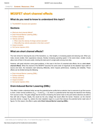
This effect is better understood when we see the potential barrier profile that an electron has to overcome to go from source
to drain. Under normal conditions ( and ), there is a potential barrier that stops the electrons from flowing
from source to drain. The gate voltage has the function of lowering this barrier down to the point where electrons are able to
flow (left side of figure). Ideally, this would be the only voltage that would affect the barrier. However, as the channel
becomes shorter, a larger widens the drain depletion region to a point that reduces the potential barrier (right side of
figure). For this reason, this effect is aptly called Drain Induced Barrier Lowering (DIBL).
= 0VDS
= 0VGS
VD
OnMyPhD
Like what you're reading? Like, +1 or tweet this page in the end. Like 353
Search...Contents | Resources || Print
2. 7/6/2018 MOSFET short channel effects
http://www.onmyphd.com/?p=mosfet.short.channel.effects 2/6
DIBL
The top figure shows a cut of a short channel (solid line) and a long-channel (dashed line) MOSFETs. The bottom part shows
the potential barrier profile along the surface of the channel (from source to drain). In the left side, , while in the
right the drain voltage is raised to show the DIBL effect.
If this a hard concept to grasp, think about it in terms of depletion regions only. The drain is close enough to the source to
easily form the depletion region normally created by the gate. That is, the drain depletion region extends to the source,
forming a unique depletion region. This is known as punchthrough. Therefore, a high drain voltage can open the bottleneck
and contribute to turn on the transistor as a gate would. This is essentially equivalent to reducing the threshold voltage of the
transistor, which leads to higher leakage current.
The DIBL effect can be calculated by measuring the threshold voltage as a function of two extreme drain voltages, :
where is a very low drain voltage and is the supply voltage (the highest drain voltage that can be applied). This
function is always positive and no DIBL effect would return 0.
Surface scattering
The velocity of the charge carriers is defined by the mobility of that carrier times the electric field along the channel. When
the carriers travel along the channel, they are atracted to the surface by the electric field created by the gate voltage. As a
result, they keep crashing and bouncing against the surface, during their travel, following a zig-zagging path. This effectively
reduces the surface mobility of the carriers, in comparison with their bulk mobility. The change in carrier mobility impacts the
current-voltage relationship of the transistor.
_
As the electron travels through the channel, it is atracted to the interface and bounces against it. This effect
reduces its mobility.
= 0VDS
( )Vth VD
DIBL =
( ) − ( )Vth V
low
D
Vth Vsupply
−Vsupply V
low
D
V
low
D
Vsupply
Si − SiO2
Like what you're reading? Like, +1 or tweet this page in the end.
3. 7/6/2018 MOSFET short channel effects
http://www.onmyphd.com/?p=mosfet.short.channel.effects 3/6
You may be wondering why this is a short-channel effect... Indeed, as the length of the channel becomes shorter, the lateral
electric field created by becomes stronger. To compensate that, the vertical electric field created by the gate voltage
needs to increase proportionally, which can be achieved by reducing the oxide thickness. As a side effect, surface scattering
becomes heavier, reducing the effective mobility in comparison with longer channel technology nodes.
Velocity saturation
The velocity of charge carriers, such as electrons or holes, is proportional to the electric field that drives them, but that is only
valid for small fields. As the field gets stronger, their velocity tends to saturate. That means that above a critical electric field,
they tend to stabilize their speed and eventually cannot move faster. Velocity saturation is specially seen in short-channel
MOSFET transistors, because they have higher electric fields.
When does the velocity of charge carriers saturate?
The critical velocity is defined by the material the charge carriers are flowing through. In particular, in diffusions it is defined
by their doping concentration. As a first-order approximation, the carrier velocity is defined as:
where is the carrier mobility, is the electric field and is the critical electric field (the point at which the velocity tends to
saturate).
The velocity saturates when and it becomes (when , as expected). In
silicon, for electrons it is ~107 cm/s and for holes around 0.6*107 cm/s.
What effect has velocity saturation in the drain current?
To see the effect of velocity saturation on transistor operation, we must see how the limit in the velocity of carriers influences
the current. We go back to see how the current is derived for the transistor model. The current is the change in charge
through time. Charge in a slice of length of the transistor is
The current is the derivative of this charge through time:
This must be true for any , since the current is equal throughout the channel. is the velocity of the carriers and it is equal
to the expression . For long channel transistor, we assume , so the difference between current with or without
velocity saturation is a division by . That is:
But velocity saturation is only apparent when the current saturates due to velocity saturation before saturating due to pinch-
off. That means that the drain-source saturation voltage will be lower than in short channel transistors. To find
out this saturation voltage, we must look for when a change in the drain-source voltage does not change the current, i.e.,
when . Differentiating with respect to and finding its zero will lead to (keep in mind that
and ):
Given that the term is positive, will be smaller than .
VDS
=vd
μE
1 + E/Ec
(1)
μ E Ec
E ≫ Ec = μ =vd Ec vsat E ≪ Ec = μEvd
dQ(x) = − W dx( − − V (x)).Cox VGS VT H
= − = .IDS
dQ(x)
dt
dQ(x)
dx
dx
dt
x
dx
dt
(1) = μEvd
1 + E/Ec
= =IDSshort
IDSlong
1 + E/Ec
μ W (( − ) − /2))Cox VGS VT H VDS V
2
DS
L(1 + E/ )Ec
(2)
−VGS VT H
d /d = 0IDS VDS (2) VDS
= /μEc vsat E = /LVDS
= .VDSSAT
2( − )VGS VT H
1 + 1 +
2μ( − )VGS VTH
Lvsat
− −−−−−−−−−−−
√
2μ( − )VGS VTH
Lvsat
VDSSAT
−VGS VT H
Like what you're reading? Like, +1 or tweet this page in the end.
4. 7/6/2018 MOSFET short channel effects
http://www.onmyphd.com/?p=mosfet.short.channel.effects 4/6
Impact ionization
As mentioned earlier, short-channel transistors create strong lateral electric fields, since the distance between source and
drain is very small. This electric field endows the charge carriers with high velocity, and therefore, high energy. The carriers
that have high enough energy to cause troubles are called "hot" carriers. These normally appear close to the drain, where
they have the most energy.
Since they are traveling through a Silicon lattice, there is a possibility that they collide with an atom of the structure. Given
enough energy, the energy passed to the atom upon collision can knock out an electron out of the valence band to the
conduction band. This originates an electron-hole pair: the hole is attracted to the bulk while the generated electron moves
on to the drain. The substrate current is a good way to measure the impact ionization effect.
_
_
+
_ _
+
+
_
_
When an electron collides with an atom of the Silicon lattice structure, the energy passed to the atom upon collision can
knock out an electron out of the valence band to the conduction band, creating an electron-hole pair. The hole is attracted to
the bulk while the generated electron moves on to the drain.
In case the generation of electron-hole pairs is very agressive, two catastrophic effects can happen. One of them relates to
the parasitic bipolar transistor that is formed by the junctions between source-bulk-drain. This transistor is normally turned off
because the bulk is biased at the lowest voltage of the circuit. However, when holes are flowing through the bulk, they are
causing a voltage drop at the parasitic resistance of the bulk itself. This, in turn, can active the BJT if the base-emitter (bulk-
source) voltage exceeds 0.6-0.7 V. With the transistor on, electrons start flowing from the source to the bulk and drain, which
can lead to even more generation of electron-hole pairs.
+
+
+
+
+
_
_
_
_
_
_
Like what you're reading? Like, +1 or tweet this page in the end.
5. 7/6/2018 MOSFET short channel effects
http://www.onmyphd.com/?p=mosfet.short.channel.effects 5/6
Holes flowing through the bulk create a voltage drop that may turn on the parasitic bipolar transistor. When it turns on,
electrons can flow to the bulk and drain by the BJT instead of the channel created by the MOSFET.
The most catastrophic case happens when the newly generated electrons become themselves hot carriers and knock out
other atoms of the lattice. This in turn can create an avalanche effect, eventually leading to an overrun current that the gate
voltage cannot control.
Hot Carrier Injection (HCI)
The hot carrier accelerated by the high electric field can have a different fate as well. The energy it contains may be sufficient
to enter the oxide and get trapped in it. The trapped electrons alter the transistor response to the gate voltage in the form of
increased threshold voltage. Over time, the accumulation of electrons in the oxide causes the so called "ageing" of
transistors. Interestingly, FLASH memories use the same effect to memorize bits: the negative charge stored in the floating
gate through injection of "hot carriers" changes the threshold voltage and this change is interpreted as a 1 or 0.
_ _ _
_
A "hot" electron manages to enter the oxide and gets trapped in it.
To reduce the formation of "hot" carriers and their negative effects, the electric field is artificially weakened with the
implantation of lighty-doped drains, beside the heavily-doped drains. The electric field only needs to be weakened at the
drain, but since the drain terminal is only defined by the operating point, the implant is added to both terminals of the
MOSFET. The reasoning here is that the depletion regions of the lightly-doped implant are wider. With wider depletion
regions there is a larger distance between different potentials, which reduces the electric field. The other side of the coin is
that the parasitic resistances of source and drain are increased.
lightly doped drain
Lightly doped drains help reduce the strength of lateral electric fields and therefore, reduce the formation of "hot" carriers.
If I helped you in some way, please help me back by liking this website on the bottom of the page or clicking on the link
below. It would mean the world to me!
TweetLike 37 ShareShare
Like what you're reading? Like, +1 or tweet this page in the end.
6. 7/6/2018 MOSFET short channel effects
http://www.onmyphd.com/?p=mosfet.short.channel.effects 6/6
Like what you're reading? Like, +1 or tweet this page in the end.