
Recommended
More Related Content
Similar to Electronic devices and circuits.pptx
Similar to Electronic devices and circuits.pptx (20)
More from ArunKumar674066
More from ArunKumar674066 (8)
Recently uploaded
Recently uploaded (20)
Electronic devices and circuits.pptx
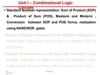
- 1. Unit I – Combinational Logic Circuits Standard Boolean representation: Sum of Product (SOP) & Product of Sum (POS), Maxterm and Minterm , Conversion between SOP and POS forms, realization using NAND/NOR gates. K-map reduction technique for the Boolean expression: Minimization of Boolean functions up to 4 variables (SOP & POS form) Design of Airthmetic circuits and code converter using K-map: Half and Full Adder, Half and Full Subtractor, Gray to Binary and Binary to Gray Code Converter (up to 4 bit). 1 9/30/2023 EA- VELTEC
- 2. Standard Representation Any logicalexpression can be expressed in the following two forms: Sum of Product (SOP) Form Product of Sum (POS) Form 9/30/2023 2 EA- VELTEC
- 3. SOP Form For Example, logical expression given is; Sum Y A.B B.C A.C Produc t 9/30/2023 3 EA- VELTEC
- 4. POS Form For Example, logical expression given is; Produc t Y ( A B).(B C).( A C ) Sum 9/30/2023 4 EA- VELTEC
- 5. Standard or Canonical SOP & POS Forms We can say that a logic expression is said to be in the standard (or canonical) SOP or POS form if each product term (for SOP) and sum term (for POS) consists of all the literals in their complemented or uncomplemented form. 9/30/2023 5 EA- VELTEC
- 6. Standard SOP Y A B C A B C A B C Each product term consists all the literals 9/30/2023 6 EA- VELTEC
- 7. Standard POS Y ( A B C).( A B C).( A B C ) Each sum term consists all the literals 9/30/2023 7 EA- VELTEC
- 8. Exampl es Sr. No. Expression Type 1 Y AB ABC ABC Non Standard SOP 2 Y AB AB AB Standard SOP 3 Y (A B).(A B).(A B) Standard POS 4 Y (A B).(A B C) Non Standard POS 9/30/2023 8 EA- VELTEC
- 9. Conversion of SOP form to Standard SOP Procedur e: 1. Write down all the terms. 2. If one or more variables are missing in any product term, expand the term by multiplying it with the sum of each one of the missing variable and its complement . 3. Drop out the redundant terms 9/30/2023 9 EA- VELTEC
- 10. Example 1 Convert given expression into its standard SOP form Y AB AC BC Y A B A C B C Missing literal is A Missing literal is B Missing literal is C Y A B . ( C C ) A C . ( B B ) B C . ( A A ) Term formed by ORing of missing literal & its complement 9/30/2023 10 EA- VELTEC
- 11. Example 1 Continue …. Y A B . ( C C ) A C . ( B B ) B C . ( A A ) Y A B C A B C A B C A B C A B C A B C Y A B C A B C A B C A B C A B C A B C Y A B C A B C A B C A B C Standard SOP form Each product term consists all the literals 9/30/2023 11 EA- VELTEC
- 12. Conversion of POS form to Standard POS Procedur e: 1. Write down all the terms. 2. If one or more variables are missing in any sum term, expand the term by adding the products of each one of the missing variable and its complement . 3. Drop out the redundant terms 9/30/2023 12 EA- VELTEC
- 13. Example 2 Convert given expression into its standard SOP form Y (A B).(AC).(B C) Term formed by ANDing of missing literal & its complement Y (A B).(AC).(B C) Missing literal is A Missing literal is B Missing literal is C Y ( A B C C ) . ( A C B B ) . ( B C A A ) 9/30/2023 13 EA- VELTEC
- 14. Example 2 Continue …. Standard POS form Each sum term consists all the literals Y ( A B C C ) . ( A C B B ) . ( B C A A ) Y (ABC)(ABC).(ABC)(ABC).(ABC)(ABC) Y (ABC)(ABC)(ABC)(ABC) Y (ABC)(ABC)(ABC)(ABC) 9/30/2023 14 EA- VELTEC
- 15. Concept of Minterm and Maxterm Minterm:Eachindividual term in the standard SOP form is called as “Minterm”. Maxterm:Each individual term in the standard POS form is called as “Maxterm”. 9/30/2023 15 EA- VELTEC
- 16. Theconceptof minterm and max term allows us to introduce a very convenient shorthand notation to express logic functions 9/30/2023 16 EA- VELTEC
- 17. Minterms & Maxterms for 3 variable/literal logic function Variables Minterms Maxterms A B C mi Mi 0 0 0 ABC m0 A B C M 0 0 0 1 ABC m1 A B C M 1 0 1 0 ABC m2 A B C M 2 0 1 1 ABC m3 A B C M 3 1 0 0 ABC m4 A B C M 4 1 0 1 ABC m5 A B C M 5 1 1 0 ABC m6 A B C M 6 1 1 1 ABC m7 A B C M 7 9/30/2023 17 EA- VELTEC
- 18. represented by mi where represented by Mi where Minterms and maxterms Each minterm is i=0,1,2,3,…….,2n-1 Each maxterm is i=0,1,2,3,…….,2n-1 If ‘n’ number of variables forms the function, then number of minterms or maxterms will be 2n • i.e. for 3 variables function f(A,B,C),the number of minterms or maxterms are 23=8 9/30/2023 18 EA- VELTEC
- 19. Minterms & Maxterms for 2 variable/literal logic function Variables Minterms Maxterms A B mi Mi 0 0 AB m0 A B M 0 0 1 AB m1 A B M 1 1 0 AB m2 A B M 2 1 1 AB m3 A B M 3 9/30/2023 19 EA- VELTEC
- 20. Representation of Logical expression using minterm Y ABC ABC ABC ABC m7 m3 m4 m5 Y m7 m3 m4 m5 Y m(3, 4,5,7) Y f (A, B,C) m(3, 4,5,7) where denotes sum of products Logical Expression 9/30/2023 20 Correspondi ng minterms O R EA- VELTEC
- 21. Representation of Logical expression using maxterm Y ( A B C).( A B C).( A B C ) M2 M0 M6 Y M 2.M 0.M6 Y M (0, 2,6) Y f (A, B,C) M (0, 2,6) where denotes product of sum Logical Expression Correspondi ng maxterms O R 9/30/2023 21 EA- VELTEC
- 22. Conversion from SOP to POS & Vice versa The relationship between the expressions using minters and maxterms is complementary. We can exploit this complementary relationship to write the expressions in terms of maxterms if the expression in terms of minterms is known and vice versa 9/30/2023 22 EA- VELTEC
- 23. Conversion from SOP to POS & Vice versa For example, if a SOP expression for 4 variable is given by, Y m(0,1, 3, 5, 6, 7,11,12,15) Then we can get expression using the equivalent POS the complementar y relationship as follows, Y M (2, 4,8, 9,10,13,14) 9/30/2023 23 EA- VELTEC
- 24. Exampl es 1.Convert the given expression into standard form Y A BC ABC 2.Convert the given expression into standard form Y (A B).(A C) 9/30/2023 24 EA- VELTEC
- 25. Unit III – Combinational Logic Circuits Standard Boolean representation: Sum of Product (SOP) & Product of Sum (POS), Maxterm and Minterm , Conversion between SOP and POS forms, realization using NAND/NOR gates. K-map reduction technique for the Boolean expression: Minimization of Boolean functions up to 4 variables (SOP & POS form) Design of Airthmetic circuits and code converter using K-map: Half and Full Adder, Half and Full Subtractor, Gray to Binary and Binary to Gray Code Converter (up to 4 bit). 9/30/2023 25 EA- VELTEC
- 26. Karnaugh Map (K-map) In the algebraic method of simplification, we need to write lengthy equations, find the common terms, manipulate the expressions etc., so it is time consuming work. Thus “K-map” is another simplification technique to reduce the Boolean equation. 9/30/2023 26 EA- VELTEC
- 27. Karnaugh Map (K-map) It overcomes all the disadvantages of algebraic simplification techniques. The information contained in a truth table or available in the SOP or POS form is represented on K-map. 9/30/2023 27 EA- VELTEC
- 28. Karnaugh Map (K-map) K-map Structure - 2 Variable A & B are variables or inputs 0 & 1 are values of A & B 2 variable k-map consists of 4 boxes i.e. 22=4 A 9/30/2023 28 B 0 1 0 1 EA- VELTEC
- 29. K-map Structure - 2 Variable Inside 4 boxes we have enter values of Y i.e. output Karnaugh Map (K- map) A B A 1 0 1 AB AB AB AB A B m0 m1 m2 m3 A 1 0 K-map & its associated minterms B B A 0 A 0 B B 1 9/30/2023 29 EA- VELTEC
- 30. Relationship between Truth Table & K- map Karnaugh Map (K- map) A B A 1 0 1 B B A 0 A B Y 0 0 0 0 1 1 1 0 0 1 1 1 0 0 1 1 B A 0 1 B 0 B 1 A A 0 1 0 1 9/30/2023 30 EA- VELTEC
- 31. Karnaugh Map (K- map) K-map Structure - 3 Variable A, B & C are variables or inputs 3 variable k-map consists of 8 boxes i.e. 23=8 AB C 0 1 B C A 0 0 0 1 0 1 11 1 0 A 9/30/2023 31 B C 0 1 0 0 0 1 11 1 0 EA- VELTEC
- 32. 3 Variable K-map & its associated product terms Karnaugh Map (K- map) A B C 0 1 B C A 0 0 0 1 0 1 11 1 0 A B C 0 1 0 0 0 1 11 1 0 0 0 0 1 11 1 0 ABC ABC ABC ABC ABC ABC ABC ABC ABC ABC ABC ABC ABC ABC ABC ABC ABC ABC ABC ABC ABC ABC ABC ABC 9/30/2023 32 EA- VELTEC
- 33. 3 Variable K-map & its associated minterms Karnaugh Map (K- map) A B C 0 1 B C A 0 m0 m1 m3 m2 m4 m5 m7 m6 00 01 11 10 m0 m2 m6 m4 m1 m3 m7 m5 00 01 11 10 1 A 9/30/2023 33 B C m0 m4 m1 m5 m3 m7 m2 m6 0 1 0 0 0 1 11 1 0 EA- VELTEC
- 34. Karnaugh Map (K- map) C D 0 0 00 01 11 10 0 1 11 1 0 A B 9/30/2023 34 0 0 0 0 0 1 0 1 11 K-map Structure - 4 Variable A, B, C & D are variables or inputs 4 variable k-map consists of 16 boxes i.e. 24=16 AB CD 1 0 11 1 0 EA- VELTEC
- 35. Karnaugh Map (K- map) A B C D 0 0 0 0 0 1 0 1 11 1 0 11 1 0 C D A B 0 0 0 0 0 1 0 1 11 1 0 11 1 0 ABCD ABCD ABCD ABCD ABCD ABCD ABCD ABCD ABCD ABCD ABCD ABCD ABCD ABCD ABCD ABCD ABCD ABCD ABCD ABCD ABCD ABCD ABCD ABCD ABCD ABCD ABCD ABCD ABCD ABCD ABCD ABCD 9/30/2023 35 4 Variable K-map and its associated product terms EA- VELTEC
- 36. Karnaugh Map (K- map) m0 m4 m12 m8 m1 m5 m13 m9 m3 m7 m15 m11 m2 m6 m11 m10 A B C D 0 0 0 0 0 1 0 1 11 1 0 11 1 0 m0 m1 m3 m2 m4 m5 m7 m6 m12 m13 m15 m14 m8 m9 m11 m10 C D 9/30/2023 36 A B 0 0 0 0 0 1 0 1 11 1 0 11 1 0 4 Variable K-map and its associated minterms EA- VELTEC
- 37. Representation of Standard SOP form expression on K-map 9/10/201 8 5 6 For example, SOP equation is given as Y ABC ABC ABC ABC ABC The given expression is in the standard SOP form. Each term represents a minterm. Wehaveto enter ‘1’ in the boxescorresponding to eachminterm as below 1 1 0 0 1 0 1 1 A 0 1 ABC ABC ABC BC BC 00 ABC ABC BC BC BC 01 11 10 A A
- 38. Simplification of K-map Once we plot the logic function or truth table on K-map, we have to use the grouping technique for simplifying the logic function. Grouping means the combining the terms in adjacent cells. The grouping of either 1’s or 0’s results in the simplification of Boolean expression. 9/30/2023 38 EA- VELTEC
- 39. Simplification of K-map If we group the adjacent1’s then the result of simplification is SOP form If we group the adjacent0’s then the result of simplification is POS form 9/30/2023 39 EA- VELTEC
- 40. Groupin g While grouping, we should group most number of 1’s. The grouping follows the binary rule i.e we can group 1,2,4,8,16,32,…..…number of 1’s. We cannot group 3,5,7,………numberof 1’s Pair: A group of two adjacent 1’s is called as Pair Quad: A group of four adjacent 1’s is called as Quad Octet: A group of eight adjacent 1’s is called as Octet 9/30/2023 40 EA- VELTEC
- 41. Grouping of Two Adjacent 1’s : Pair A pair eliminates 1 variable 0 0 1 1 0 0 0 0 B C A 0 1 BC 11 BC 00 BC 0 1 BC 10 A A ABC ABC Y ABC ABC Y AB(C C) Y AB ( C C 1) 9/30/2023 41 EA- VELTEC
- 42. 0 0 0 0 1 0 0 1 B C A 0 1 BC 11 BC 00 BC 0 1 BC 10 A A 0 1 0 0 0 1 0 0 B C A 0 1 BC 11 BC 00 BC 0 1 BC 10 A A 1 1 1 0 B A 0 1 B 1 B 0 A A B C A BC BC BC BC 00 01 11 10 0 1 1 1 0 0 1 0 0 1 A A Grouping of Two Adjacent 1’s : Pair 9/30/2023 42 EA- VELTEC
- 43. 0 1 0 0 0 0 0 0 0 0 0 0 0 1 0 0 C D CD CD CD 00 01 11 10 C D AB AB 00 0 1 11 1 0 AB AB AB Grouping of Two Adjacent 1’s : Pair 9/30/2023 43 EA- VELTEC
- 44. Possible Grouping of Four Adjacent 1’s : Quad 0 0 0 0 0 0 0 0 0 0 0 0 1 1 1 1 C D AB CD 11 CD 00 CD 01 CD 10 AB 0 0 0 1 11 1 0 AB AB AB 0 1 0 0 0 1 0 0 0 1 0 0 0 1 0 0 C D AB CD 11 CD 00 CD 01 CD 10 AB 0 0 0 1 11 1 0 AB AB AB A Quad eliminates 2 variable 9/30/2023 44 EA- VELTEC
- 45. Possible Grouping of Four Adjacent 1’s : Quad 0 0 0 0 1 1 0 0 1 1 0 0 0 0 0 0 C D AB CD 00 CD 01 CD 11 CD 10 AB 0 0 0 1 11 1 0 AB AB AB 0 1 1 0 0 0 0 0 0 0 0 0 0 1 1 0 C D AB CD 00 CD 01 CD 11 CD 10 AB 0 0 0 1 11 1 0 AB AB AB A Quad eliminates 2 variable 9/30/2023 45 EA- VELTEC
- 46. Possible Grouping of Four Adjacent 1’s : Quad 0 0 0 0 1 0 0 1 1 0 0 1 0 0 0 0 C D AB CD 11 CD 00 CD 01 CD 10 AB 0 0 0 1 11 1 0 AB AB AB A Quad eliminates 2 variable 1 0 0 1 0 0 0 0 0 0 0 0 1 0 0 1 9/30/2023 46 C D AB CD 00 CD 01 CD 11 CD 10 AB 0 0 0 1 11 1 0 AB AB AB EA- VELTEC
- 47. Possible Grouping of Four Adjacent 1’s : Quad 0 0 0 0 0 1 1 1 0 1 1 1 0 0 0 0 C D AB CD 00 CD 01 CD 11 CD 10 AB 0 0 0 1 11 1 0 AB AB AB 0 0 0 0 0 1 1 0 0 1 1 0 0 1 1 0 C D AB CD 00 CD 01 CD 11 CD 10 AB 0 0 0 1 11 1 0 AB AB AB A Quad eliminates 2 variable 9/30/2023 47 EA- VELTEC
- 48. Possible Grouping of Eight Adjacent 1’s : Octet 0 0 0 0 0 0 0 0 1 1 1 1 1 1 1 1 C D AB CD 00 CD 01 CD 11 CD 10 AB 0 0 0 1 11 1 0 AB AB AB 0 1 1 0 0 1 1 0 0 1 1 0 0 1 1 0 C D AB CD 00 CD 01 CD 11 CD 10 AB 0 0 0 1 11 1 0 AB AB AB A Octet eliminates 3 variable 9/30/2023 48 EA- VELTEC
- 49. Possible Grouping of Eight Adjacent 1’s : Octet 1 0 0 1 1 0 0 1 C D AB 00 01 11 10 1 0 0 1 1 0 0 1 CD CD CD CD AB 0 0 0 1 11 1 0 AB AB AB A Octet eliminates 3 variable 1 1 1 1 0 0 0 0 0 0 0 0 1 1 1 1 9/30/2023 49 C D AB CD 00 CD 01 CD 11 CD 10 AB 0 0 0 1 11 1 0 AB AB AB EA- VELTEC
- 50. Rules for K-map simplification 1. Groups may not include any cell containing a zero. 0 1 A B 0 1 B B A 1 A 0 0 1 1 A B 0 1 B B A 1 A 0 Not Accepted 9/30/2023 50 Accepte d EA- VELTEC
- 51. Rules for K-map simplification 2. Groups may be horizontal or vertical, but may not be diagonal 0 1 1 0 A B 0 1 B B A 1 A 0 0 1 1 1 A B 0 1 B B A 1 A 0 Not Accepted 9/30/2023 51 Accepte d EA- VELTEC
- 52. Rules for K-map simplification 3. Groups must contain 1,2,4,8 or in general 2n cell s 9/10/201 8 7 1 1 1 0 1 A B 0 1 B B A 1 A 0 1 1 0 1 A B 0 1 B B A 1 A 0 Not Accepte 0 1 1 1 0 0 0 0 B C A 0 1 BC 11 BC 00 BC 0 1 BC 10 A A 0 1 1 1 0 0 0 0 B C A 0 1 BC 11 BC 00 BC 0 1 BC 10 A A
- 53. Rules for K-map simplification 4. Each group should be as large as possible Not Accepted Accepte d 1 1 1 1 0 0 1 1 B C A 0 1 BC 11 BC BC 00 0 1 BC 10 A A 1 1 1 1 0 0 1 1 B C A 0 1 BC 11 BC BC 00 0 1 BC 10 A A 9/30/2023 53 EA- VELTEC
- 54. Rules for K-map simplification 5. Each cell containing a one must be in at least one group 0 0 0 1 0 0 1 0 B C A 0 1 BC 11 BC BC 00 0 1 BC 10 A A 9/30/2023 54 EA- VELTEC
- 55. Rules for K-map simplification 6. Groups may be overlap 1 1 1 1 0 0 1 1 B C A 0 1 BC BC 00 0 1 BC 11 BC 10 A A 9/30/2023 55 EA- VELTEC
- 56. Rules for K-map simplification 7. Groups may wrap around the table. The leftmost cell in a row may be grouped with rightmost cell and the top cell in a column may be grouped with bottomcell 1 0 0 1 1 0 0 1 B C A 0 1 BC 11 BC 00 BC 0 1 BC 10 A A 1 1 1 1 0 0 0 0 0 0 0 0 1 1 1 1 9/30/2023 56 C D AB CD 00 CD 01 CD 11 CD 10 AB 0 0 0 1 11 1 0 AB AB AB EA- VELTEC
- 57. Rules for K-map simplification 8. There should be as few groups as possible, as long as this does not contradict any of the previousrules. Not Accepted Accepte d 1 1 1 1 0 0 1 1 B C A 0 1 BC 11 BC BC 00 0 1 BC 10 A A 1 1 1 1 0 0 1 1 B C A 0 1 BC 11 BC BC 00 0 1 BC 10 A A 9/30/2023 57 EA- VELTEC
- 58. Rules for K-map simplification 9. A pair eliminates one variable. 10.A Quad eliminates two variables. 11.A octet eliminates three variables 9/30/2023 58 EA- VELTEC
- 59. Example 1 For the given K-map write simplified Boolean expression 0 1 1 1 0 0 1 0 C 1 AB 11 AB AB 00 AB 0 1 AB 10 C 0 C 9/30/2023 59 EA- VELTEC
- 60. Example 1 continue ….. A B C 1 C 0 C AB AB AB AB 00 01 11 10 0 1 1 1 AC 0 0 1 0 AB BC Simplified Boolean expression Y BC AB AC 9/30/2023 60 EA- VELTEC
- 61. Example 2 For the given K-map write simplified Boolean expression 1 1 0 1 1 0 0 1 C 1 AB 11 AB AB 00 AB 0 1 AB 10 C 0 C 9/30/2023 61 EA- VELTEC
- 62. Example 2 continue ….. 1 1 0 1 1 0 0 1 C 1 AB 11 AB AB 00 AB 0 1 AB 10 C 0 C AC Simplified Boolean expression B Y B AC 9/30/2023 62 EA- VELTEC
- 63. Example 3 A logical expression in the standard SOP form is as follows; Minimize it with using the K-map technique Y A B C A B C A B C A B C 9/30/2023 63 EA- VELTEC
- 64. Example 3 continue …… Y A B C A B C A B C A B C B C A 0 1 A A BC BC BC BC AB 00 01 11 10 1 0 1 1 0 1 0 0 AC ABC Simplified Boolean expression Y AC AB ABC 9/30/2023 64 EA- VELTEC
- 65. Example 4 A logical expression representing a logic circuit is; Y m ( 0 , 1 , 2 , 5 , 1 3 , 1 5 ) Draw the K-map and find the minimized logical expression 9/30/2023 65 EA- VELTEC
- 66. Example 4 continue ….. Y m ( 0 , 1 , 2 , 5 , 1 3 , 1 5 ) C D AB CD 11 CD 00 CD 01 CD 10 AB 0 0 0 1 11 1 0 AB AB AB 0 1 1 1 3 0 2 1 4 0 5 1 7 0 6 0 12 0 13 1 15 1 14 0 8 0 9 0 11 0 10 0 ABD ABD ACD Y A B D ACD ABD 9/30/2023 66 Simplified Boolean expression EA- VELTEC
- 67. Example 5 Minimize the following Boolean expression using K-map ; f (A, B,C, D) m(1,3,5,9,11,13) 9/30/2023 67 EA- VELTEC
- 68. Example 5 continue ….. C D AB CD 00 CD 01 CD 11 CD 10 AB 0 0 0 1 11 1 0 AB AB AB 2 6 0 0 1 1 1 3 0 4 0 5 1 0 7 0 12 0 13 1 1 5 0 1 4 0 8 9 11 10 0 1 1 0 CD BD Simplified Boolean expression f ( A , B , C , D ) m ( 1 , 3 , 5 , 9 , 11 , 1 3 ) f BD C D f D ( B C) 9/30/2023 68 EA- VELTEC
- 69. Example 6 Minimize the following Boolean expression using K-map ; f (A, B,C, D) m(4,5,8,9,11,12,13,15) 9/30/2023 69 EA- VELTEC
- 70. Example 6 continue ….. C D AB 0 0 1 0 3 0 2 0 4 1 5 1 7 0 6 0 12 1 13 1 15 1 14 0 8 1 9 1 11 1 10 0 C D CD CD CD 00 01 11 10 AB 0 0 0 1 11 1 0 AB AB AB AD AC f BC AC AD Simplified Boolean expression f (A, B,C, D) m(4,5,8,9,11,12,13,15) BC 9/30/2023 70 EA- VELTEC
- 71. Example 7 Minimize the following Boolean expression using K-map ; f 2(A, B,C, D) m(0,1,2,3,11,12,14,15) 9/30/2023 71 EA- VELTEC
- 72. Example 7 continue ….. C D AB CD 00 AB CD 01 CD 11 CD 10 AB 0 0 0 1 11 1 0 AB AB AB ABD f 2 AB A B D ACD Simplified Boolean expression f 2(A, B,C, D) m(0,1,2,3,11,12,14,15) 1 0 1 1 3 1 1 2 0 4 5 0 7 0 0 6 1 2 1 13 0 15 1 1 4 1 0 8 9 0 11 1 1 0 0 9/30/2023 72 ACD EA- VELTEC
- 73. Example 8 Solve the following expression with K- maps; 1 . 2 . f 1(A, B,C) m(0,1,3,4,5) f 2(A, B,C) m(0,1,2,3,6,7) 9/30/2023 73 EA- VELTEC
- 74. Example 8 continue …… f 1(A, B,C) m(0,1,3, 4,5) f 2( A, B , C ) m(0,1, 2,3, 6, 7) 1 1 1 0 1 1 0 0 B C A 0 1 BC BC 00 0 1 BC 11 A A 0 1 3 2 4 5 7 6 1 1 1 1 0 0 1 1 B C A 0 1 BC 00 BC 0 1 BC 11 BC 10 A A 0 1 3 2 4 5 7 6 AC BC 10 B B A f 2 A B Simplified Boolean expression f 1 AC B 9/30/2023 74 Simplified Boolean expression EA- VELTEC
- 75. Example 9 Simplify ; f (A, B,C, D) m(0,1,4,5,7,8,9,12,13,15) 9/30/2023 75 EA- VELTEC
- 76. Example 9 continue ….. C D CD CD CD 00 01 11 10 C D AB AB 00 0 1 1 1 3 0 2 0 4 1 5 1 7 1 6 0 12 1 13 1 15 1 14 0 8 1 9 1 11 0 10 0 0 1 11 1 0 AB AB AB BD C f C BD Simplified Boolean expression f (A, B,C, D) m(0,1,4,5,7,8,9,12,13,15) 9/30/2023 76 EA- VELTEC
- 77. Example 10 Solve the following expression with K- maps; 1 . 2 . f 1(A, B,C, D) m(0,1,3,4,5,7) f 2(A, B,C) m(0,1,3,4,5,7) 9/30/2023 77 EA- VELTEC
- 78. Example 10 continue …… 1 1 1 0 1 1 1 0 B C A 0 1 BC 00 BC 0 1 BC 11 BC 10 A A 0 1 3 2 4 5 7 6 C B f 2 B C Simplified Boolean expression Simplified Boolean expression f 1 AC AD f 1(A, B,C, D) m(0,1,3,4,5,7) f 2(A, B,C) m(0,1,3, 4,5, 7) C D AB 0 1 1 1 3 0 2 0 4 1 5 1 7 1 6 0 12 0 13 0 15 0 14 0 8 0 9 0 11 0 10 0 CD 11 CD 00 CD 01 CD 10 AB 0 0 0 1 11 1 0 AB AD AB AB AC 9/30/2023 78 EA- VELTEC
- 79. K-map for Product of Sum Form (POS Expressions) Karnaughmap can also be used for Boolean expression in the Product of sum form (POS). The procedure for simplification of expression by grouping of cells is also 9/30/2023 79 EA- VELTEC
- 80. The letters with bars (NOT)represent 1 and unbarred letters represent 0 of Binary. A zero is put in the cell for which there is a term in the Boolean expression Grouping is done for adjacent cells containing zeros. K-map for Product of Sum Form (POS Expressions) 9/30/2023 80 EA- VELTEC
- 81. Example 11 Simplify ; f (A, B,C, D) M (0,1,3,5,6,7,10,14,15) 9/30/2023 81 EA- VELTEC
- 82. Example 11 continue ….. C D AB CD 00 CD 01 CD 11 CD 10 0 0 1 0 3 0 2 1 4 1 5 0 7 0 6 0 12 1 13 1 15 0 14 0 8 1 9 1 11 1 10 0 0 0 AB 0 1 11 1 0 AB AB AB ACD ABC Simplified Boolean expression f ( A D)(B C)( A C D)( A B C) f (A, B,C, D) M (0,1,3,5,6,7,10,14,15) AD BC 9/30/2023 82 EA- VELTEC
- 83. Example 12 Simplify ; f (A, B,C, D) M (4,6,10,12,13,15) 9/30/2023 83 EA- VELTEC
- 84. Example 12 continue ….. 1 1 0 1 1 0 0 1 1 1 0 C D AB CD 00 CD 01 CD 11 CD 10 0 0 AB 0 1 11 1 0 AB AB AB 0 1 1 3 2 1 4 5 7 6 8 9 11 1 0 1 2 1 3 0 1 5 0 1 4 1 ABCD ABC ABD f (A, B,C, D) M (4,6,10,12,13,15) ABD Simplified Boolean expression f ( A B C D)( A B D)( A B D)( A B C) 9/30/2023 84 EA- VELTEC
- 85. K-map and don’t care conditions For SOP form we enter 1’s corresponding to the combinations of input variables which produce a high output and we enter 0’s in the remaining cells of the K-map. For POS form we enter 0’s corresponding to the combinations of input variables which produce a high output and we enter 1’s in the remaining cells of the K-map. 9/30/2023 85 EA- VELTEC
- 86. But it is not always true that the cells not containing 1’s (in SOP) will contain 0’s, because some combinations of input variable do not occur. Also for some functions the outputs corresponding to certain combinations of input variables do not matter. K-map and don’t care conditions 9/30/2023 86 EA- VELTEC
- 87. In such situations we have a freedom to assume a 0 or 1 as output for each of these combinations. These conditions are known as the “Don’t Care Conditions” and in the K-map it is represented as ‘X’, in the corresponding cell. The don’t care conditions may be assumed to be 0 or 1 as per the need for simplification K-map and don’t care conditions 9/30/2023 87 EA- VELTEC
- 88. K-map and don’t care conditions - Example 9/30/2023 88 Simplify ; f (A, B,C, D) m(1,3,7,11,15) d(0,2,5) EA- VELTEC
- 89. C D CD CD CD 00 01 11 10 C D AB AB 00 0 1 11 1 0 AB AB AB AB f CD AB AD Simplified Boolean expression 0 X 1 1 3 1 2 X 4 0 5 X 7 1 6 0 12 0 13 0 15 1 1 4 0 8 0 9 0 11 1 1 0 0 CD K-map and don’t care conditions - Example f (A, B,C, D) m(1,3, 7,11,15) d(0, 2,5) AD 9/30/2023 89 EA- VELTEC
- 90. Unit III – Combinational Logic Circuits Standard Boolean representation: Sum of Product (SOP) & Product of Sum (POS), Maxterm and Minterm , Conversion between SOP and POS forms, realization using NAND/NOR gates. K-map reduction technique for the Boolean expression: Minimization of Boolean functions up to 4 variables (SOP & POS form) Design of Airthmetic circuits and code converter using K-map: Half Adder and Full Adder, Half and Full Subtractor, Gray to Binary and Binary to Gray Code Converter (up to 4 bit). 9/30/2023 90 EA- VELTEC
- 91. Half Adder Half adder is a combinational logic circuit with two inputs and two outputs. It is a basic building block for addition of two single bit numbers. Half Adde r 9/30/2023 91 A B Su m Carr y Input s Output s EA- VELTEC
- 92. Half Adder 9/30/2023 92 Input Output A B Sum (S) Carry (C) 0 0 0 0 0 1 1 0 1 0 1 0 1 1 0 1 Truth Table for Half Adder EA- VELTEC
- 93. Half Adder K-map for Sum Output: 0 1 1 0 A B A 1 0 1 B B A 0 0 0 0 1 A B A 1 0 1 B B A 0 K-map for Carry Output: S AB AB S A B 9/30/2023 93 C AB EA- VELTEC
- 94. Half Adder Logic Diagram: A B S A B 9/30/2023 94 C AB EA- VELTEC
- 95. Half Adder Logic Diagram using Basic Gates: A B S A B 9/30/2023 95 C AB EA- VELTEC
- 96. Unit III – Combinational Logic Circuits Standard Boolean representation: Sum of Product (SOP) & Product of Sum (POS), Maxterm and Minterm , Conversion between SOP and POS forms, realization using NAND/NOR gates. K-map reduction technique for the Boolean expression: Minimization of Boolean functions up to 4 variables (SOP & POS form) Design of Airthmetic circuits and code converter using K-map: Half and Full Adder, Half and Full Subtractor, Gray to Binary and Binary to Gray Code Converter (up to 4 bit). 9/30/2023 96 EA- VELTEC
- 97. Full Adder Full adder is a combinationallogic circuit with three inputs and two outputs. Full Adde r A B Su m Carr y Input s Output s Ci n 9/30/2023 97 EA- VELTEC
- 98. Full Adder 9/30/2023 98 Truth Table Inputs Outputs A B Cin Sum (S) Carry (C) 0 0 0 0 0 0 0 1 1 0 0 1 0 1 0 0 1 1 0 1 1 0 0 1 0 1 0 1 0 1 1 1 0 0 1 1 1 1 1 1 EA- VELTEC
- 99. Full Adder K-map for Sum Output: 0 1 0 1 1 0 1 0 B C A 0 1 BC 11 BC 00 BC 0 1 BC 10 A A ABC ABC ABC ABC S ABC ABC ABC ABC S ABC ABC ABC ABC S C( AB AB) C( AB AB) Let AB AB X S C( X ) C( X ) S C X Let X A B S C A B 9/30/2023 99 EA- VELTEC
- 100. Full Adder K-map for Carry Output: C AB BC AC 0 0 1 0 0 1 1 1 B C A 0 1 BC 11 BC 00 BC 0 1 BC 10 A A BC AB 9/30/2023 100 AC EA- VELTEC
- 101. Full Adder Logic Diagram: A B C S A BC 9/30/2023 101 C A B B C A C EA- VELTEC
- 102. Full Adder using Half Adders A 9/30/2023 102 B C HA1 HA2 S0 S1 C0 C1 Carry Sum EA- VELTEC
- 103. Unit III – Combinational Logic Circuits Standard Boolean representation: Sum of Product (SOP) & Product of Sum (POS), Maxterm and Minterm , Conversion between SOP and POS forms, realization using NAND/NOR gates. K-map reduction technique for the Boolean expression: Minimization of Boolean functions up to 4 variables (SOP & POS form) Design of Airthmetic circuits and code converter using K-map: Half and Full Adder, Half Subtractor and Full Subtractor, Gray to Binary and Binary to Gray Code Converter (up to 4 bit). 9/30/2023 103 EA- VELTEC
- 104. Half Subtractor Half subtractor is a combinationallogic circuit with two inputs and two outputs. It is a basic building block for subtraction of two single bit numbers. Half Subtract or 9/30/2023 104 A B Differenc e Borro w Input s Output s EA- VELTEC
- 105. Input Output A B Difference (D) Borrow (B) 0 0 0 0 0 1 1 1 1 0 1 0 1 1 0 0 9/30/2023 105 Truth Table Half Subtractor EA- VELTEC
- 106. K-map for Difference Output: 0 1 1 0 A B A 1 0 1 B B A 0 0 1 0 0 A B A 1 0 1 B B A 0 K-map for Borrow Output: D AB AB D A B B AB 9/30/2023 106 Half Subtractor EA- VELTEC
- 107. Half Subtractor Logic Diagram: A B D A B B AB 9/30/2023 107 EA- VELTEC
- 108. Half Subtractor Logic Diagram using Basic Gates: A B D A B B AB 9/30/2023 108 EA- VELTEC
- 109. Unit III – Combinational Logic Circuits Standard Boolean representation: Sum of Product (SOP) & Product of Sum (POS), Maxterm and Minterm , Conversion between SOP and POS forms, realization using NAND/NOR gates. K-map reduction technique for the Boolean expression: Minimization of Boolean functions up to 4 variables (SOP & POS form) Design of Airthmetic circuits and code converter using K-map: Half and Full Adder, Half and Full Subtractor, Gray to Binary and Binary to Gray Code Converter (up to 4 bit). 9/30/2023 109 EA- VELTEC
- 110. Full Subtractor Full subtractor is a combinational logic circuit with three inputs and two outputs. Full Subtract or A B Differenc e Borro w Input s Output s Bi n 9/30/2023 110 EA- VELTEC
- 111. Full Subtractor 9/30/2023 111 Truth Table Inputs Outputs A B Bin (C) Difference (D) Borrow (B0) 0 0 0 0 0 0 0 1 1 1 0 1 0 1 1 0 1 1 0 1 1 0 0 1 0 1 0 1 0 0 1 1 0 0 0 1 1 1 1 1 EA- VELTEC
- 112. Full Subtractor K-map for Difference Output: 0 1 0 1 1 0 1 0 B C A 0 1 BC 11 BC 00 BC 0 1 BC 10 A A ABC ABC ABC ABC D ABC ABC ABC ABC D ABC ABC ABC ABC D C( AB AB) C( AB AB) Let AB AB X D C( X ) C( X ) D C X Let X A B D C A B 9/30/2023 112 EA- VELTEC
- 113. Full Subtractor K-map for Borrow Output: B0 AB BC AC 0 1 1 1 0 0 1 0 B C A 0 1 BC 11 BC 00 BC 0 1 BC 10 A A BC AB AC 9/30/2023 113 EA- VELTEC
- 114. Full Subtractor Logic Diagram: A B C D A BC B0 AB B C AC 9/30/2023 114 EA- VELTEC
- 115. Full Subtractor using Half Subtractor A 9/30/2023 115 B C HS1 HS2 D0 D1 B0 B1 Borrow Difference EA- VELTEC
- 116. Unit III – Combinational Logic Circuits Standard Boolean representation: Sum of Product (SOP) & Product of Sum (POS), Maxterm and Minterm , Conversion between SOP and POS forms, realization using NAND/NOR gates. K-map reduction technique for the Boolean expression: Minimization of Boolean functions up to 4 variables (SOP & POS form) Design of Airthmetic circuits and code converter using K-map: Half and Full Adder, Half and Full Subtractor, Gray to Binary Code Converter and Binary to Gray Code Converter (up to 4 bit). 9/30/2023 116 EA- VELTEC
- 117. Design of Gray to Binary Code Converter Block Diagram: Gray to Binary Code converter B 3 Binary Output s Gray Input s B 9/30/2023 117 2 B 1 B 0 G 3 G2 G 1 G 0 EA- VELTEC
- 118. Design of Gray to Binary Code Converter Gray Inputs Binary Outputs G3 G2 G1 G0 B3 B2 B1 B0 0 0 0 0 0 0 0 0 0 0 0 1 0 0 0 1 0 0 1 0 0 0 1 1 0 0 1 1 0 0 1 0 0 1 0 0 0 1 1 0 0 1 0 1 0 1 1 1 0 1 1 0 0 1 0 1 0 9 1 /10/201 8 1 1 0 1 0 0 Amit Gray Inputs Binary Outputs G3 G2 G1 G0 B3 B2 B1 B0 1 0 0 0 1 1 0 0 1 0 0 1 1 1 0 1 1 0 1 0 1 1 1 1 1 0 1 1 1 1 1 0 1 1 0 0 1 0 1 0 1 1 0 1 1 0 1 1 1 1 1 0 1 0 0 1 1 vase 1 1 1 1 0 0 137 0 Truth Table : N e 9/30/2023 EA- VELTEC
- 119. K-map for B0: 0 0 1 1 3 0 2 1 4 1 5 0 7 1 6 0 12 0 13 1 15 0 14 1 8 1 9 0 11 1 10 0 G1G0 11 G3G2 0 0 0 1 11 1 0 G1G 0 G3G2 GG2 3 G3G2 G3G2 G1G0 G1 G0 00 01 G1G0 10 B 0 G 3 G 2 G 1 G 0 G 3 G 2 G 1 G 0 G 3 G 2 G 1 G 0 G 3 G 2 G 1 G 0 G 3 G 2 G 1 G 0 G 3 G 2 G 1 G 0 G 3 G 2 G 1 G 0 G 3 G 2 G 1 G 0 B 0 G 3 G 2 G 1 G 0 9/30/2023 Design of Gray to Binary Code Converter EA- VELTEC
- 120. K-map for B1: 0 0 1 0 3 1 2 1 4 1 5 1 7 0 6 0 12 0 13 0 15 1 14 1 8 1 9 1 11 0 10 0 G1G 0 G3G2 G1G0 11 G3G2 0 0 0 1 11 1 0 GG2 3 G3G2 G3G2 G1G0 G1 G0 00 01 G1G0 10 B1 G 3 G 2 G 1 G 3 G 2 G 1 G 3 G 2 G 1 G 3 G 2 G 1 B1 G 3 G 2 G 1 Design of Gray to Binary Code Converter 9/30/2023 EA- VELTEC
- 121. K-map for B2: 0 0 1 0 3 0 2 0 4 1 5 1 7 1 6 1 12 0 13 0 15 0 14 0 8 1 9 1 11 1 10 1 G1G 0 G3G2 G1G0 11 G3G2 0 0 0 1 11 1 0 GG2 3 G3G2 G3G2 G1G0 G1 G0 00 01 G1G0 10 B 2 G 3 G 2 G 3 G 2 B1 G 3 G 2 Design of Gray to Binary Code Converter 9/30/2023 EA- VELTEC
- 122. K-map for B3: 0 0 1 0 3 0 2 0 4 0 5 0 7 0 6 0 12 1 13 1 15 1 14 1 8 1 9 1 11 1 10 1 G1G 0 G3G2 G1G0 11 0 0 G3G2 0 1 11 1 0 GG2 3 G3G2 G3G2 G1G0 G1 G0 00 01 G1G0 10 B 3 G 3 Design of Gray to Binary Code Converter 9/30/2023 EA- VELTEC
- 123. Logic Diagram: G3 G2 G1 G0 9/30/2023 B2 G3 G2 B1 G1 G2 G3 B0 G0 G1 G2 G3 B3 Design of Gray to Binary Code Converter EA- VELTEC
- 124. Unit III – Combinational Logic Circuits Standard Boolean representation: Sum of Product (SOP) & Product of Sum (POS), Maxterm and Minterm , Conversion between SOP and POS forms, realization using NAND/NOR gates. K-map reduction technique for the Boolean expression: Minimization of Boolean functions up to 4 variables (SOP & POS form) Design of Airthmetic circuits and code converter using K-map: Half and Full Adder, Half and Full Subtractor, Gray to Binary and Binary to Gray Code Converter (up to 4 bit). 9/30/2023 EA- VELTEC
- 125. Design of Binary to Gray Code Converter Block Diagram: Binary to Gray Code converter B 3 Binar y Input s Gray Output s 2 9/30/2023 B B1 B 0 G 3 2 G G1 G 0 EA- VELTEC
- 126. Design of Binary to Gray Code Converter Binary Inputs Gray Outputs B3 B2 B1 B0 G3 G2 G1 G0 0 0 0 0 0 0 0 0 0 0 0 1 0 0 0 1 0 0 1 0 0 0 1 1 0 0 1 1 0 0 1 0 0 1 0 0 0 1 1 0 0 1 0 1 0 1 1 1 0 1 1 0 0 1 0 1 0 /10/ 1 201 8 1 1 0 1 0 0t Binary Inputs Gray Outputs B3 B2 B1 B0 G3 G2 G1 G0 1 0 0 0 1 1 0 0 1 0 0 1 1 1 0 1 1 0 1 0 1 1 1 1 1 0 1 1 1 1 1 0 1 1 0 0 1 0 1 0 1 1 0 1 1 0 1 1 1 1 1 0 1 0 0 1 va 1e 1 1 1 1 0 0 145 0 Truth Table : N e EA- VELTEC
- 127. Design of Binary to Gray Code Converter K-map for G0: B3B 2 0 0 1 1 3 0 2 1 4 0 5 1 7 0 6 1 12 0 13 1 15 0 14 1 8 0 9 1 11 0 10 1 B1B0 11 B3B2 0 0 0 1 11 1 0 B B 1 0 B B2 3 B3B2 B3B2 B1B0 B1B0 00 01 B1B0 10 B1B0 B1B0 G0 B1B0 B1B0 G0 B0 B1 9/30/2023 EA- VELTEC
- 128. Design of Binary to Gray Code Converter K-map for G1: B3B 2 0 0 1 0 3 1 2 1 4 1 5 1 7 0 6 0 12 1 13 1 15 0 14 0 8 0 9 0 11 1 10 1 B3B2 0 0 0 1 11 1 0 B B 1 0 B1B0 11 B B2 3 B3B2 B3B2 B1B0 B1B0 00 01 B1B0 10 B2B1 G1 B2B1 B2B1 G1 B2 B1 B2B1 9/30/2023 EA- VELTEC
- 129. Design of Binary to Gray Code Converter K-map for G2: 0 0 1 1 1 1 0 0 0 0 1 1 1 B3B 2 B3B2 0 0 0 1 11 1 0 0 1 0 3 2 0 4 5 7 6 8 9 11 1 0 1 1 2 1 3 1 5 1 4 B B 1 0 B B2 3 B3B2 B3B2 B1B0 B1B0 00 01 B1B0 11 B1B0 10 B3B2 G2 B3B2 B3B2 G2 B3 B2 B3B2 9/30/2023 EA- VELTEC
- 130. Design of Binary to Gray Code Converter K-map for G3: B3B 2 0 0 1 0 3 0 2 0 4 0 5 0 7 0 6 0 12 1 13 1 15 1 14 1 8 1 9 1 11 1 10 1 B1B0 11 B3B2 0 0 0 1 11 1 0 B B 1 0 B B2 3 B3B2 B3B2 B1B0 B1B0 00 01 B1B0 10 B3 G3 B3 9/30/2023 EA- VELTEC
- 131. Design of Binary to Gray Code Converter Logic Diagram: B3 B2 B1 B0 9/30/2023 G2 B3 B2 G1 B2 B1 G0 B1B0 G3 EA- VELTEC
- 132. Unit III – Combinational Logic Circuits Airthmetic Circuits: (IC 7483) Adder & Subtractor, BCD Adder Encoder/Decoder: Basics of Encoder, decoder, comparison, (IC 7447) BCD to 7- Segment decoder/driver. Multiplexer and Demultiplexer: Working, truth table and applications of Multiplexers and Demultiplexers, MUX tree, IC 74151 as MUX, DEMUX tree, DEMUX as decoder, IC 74155 as DEMUX Buffer: Tristate logic, Unidirectional and Bidirectional buffer (IC 74LS244 and IC 74LS245) 9/30/2023 EA- VELTEC
- 133. N – Bit Parallel Adder The full adder is capable of adding two single digit binary numbers along with a carry input. But in practice we need to add binary numbers which are much longer than one bit. To add two n-bit binary numbers we need to use the n-bit parallel adder. It uses a number of full adders in cascade. The carry output of the previous full adder is connected to the carry input of the next full adder.. 9/30/2023 EA- VELTEC
- 134. N – Bit Parallel Adder A0 B 0 9/30/2023 A1 A2 An 1 Bn 1 B1 B 2 S 0 S1 S 2 Sn 1 C 0 Cin FA-0 FA-1 FA-2 FA-(n-1) EA- VELTEC
- 135. 4 – Bit Parallel Adder using full adder A0 B 0 9/30/2023 A1 A2 A3 B1 B 2 B3 S 0 S1 S 2 S 3 C 0 Cin FA-0 FA-1 FA-2 FA-3 EA- VELTEC
- 136. IC 7483 4 – Bit Binary Parallel Adder A0 B 0 9/30/2023 A1 A2 A3 B1 B 2 B3 S 0 S1 S 2 S 3 C 0 Cin FA-0 FA-1 FA-2 FA-3 EA- VELTEC
- 137. IC 7483 4 – Bit Binary Parallel Adder Sum Output IC 7483 A1 A0 A3 A2 B Binary number B3 B2 B1 B0 S1 S 0 S 3 S 2 Cin Carr y Input C0 Carry Outpu t 9/30/2023 A Binary number EA- VELTEC
- 138. Cascading of IC 7483 IC 7483-II Higher nibble of A Binary number A7 A6 A5 A4 Higher nibble of B Binary number B7 B6 B5 B4 S 5 S 4 S 7 S 6 C in C 0 Carry Outpu t Sum Output IC 7483-I Lower nibble of A Binary number A3 A2 A1 A0 B3 B2 B1 B0 S1 S 0 S 3 S 2 C 0 C in Carr y Inpu t Lower nibble of B Binary number If we want to add two 8 bit binary numbers using 4 bit binary parallel adder IC 7483, then we have to cascade the two ICs in following way 9/30/2023 EA- VELTEC
- 139. Design of 1 Digit BCD Adder Block Diagram: 9/10/201 8 15 8 Logic Circuit IC 7483-I IC 7483-II Add 0110 Command Cin C 0 Cin C 0 A BCD no. B BCD no. S 3 S 2 S1 S 0 S 3 S 2 S1 S 0
- 140. Design of 1 Digit BCD Adder As we know BCD addition rules, we understand that the 4 bit BCD adder should consists of following: A 4 bit binary adder to add the given two (4 bit numbers). A combinational logic circuit to check if sum is greater than 9 or carry 1. One more 4 bit binary adder to add 0110 to the invalid BCD sum or if carry is 1 9/30/2023 EA- VELTEC
- 141. Design of 1 Digit BCD Adder Logic Table for design of Logic circuit: Inputs Y S3 S2 S1 S0 0 0 0 0 0 0 0 0 1 0 0 0 1 0 0 0 0 1 1 0 0 1 0 0 0 0 1 0 1 0 0 1 1 0 0 0 1 1 1 0 Inputs Y S3 S2 S1 S0 1 0 0 0 0 1 0 0 1 0 1 0 1 0 1 1 0 1 1 1 1 1 0 0 1 1 1 0 1 1 1 1 1 0 1 1 1 1 1 1 Sum is invali d BCD Numbe r Y=1 9/30/2023 EA- VELTEC
- 142. Design of 1 Digit BCD Adder K-map for Logic circuit: 0 0 0 0 0 0 0 0 1 1 1 1 0 0 1 1 S3s 2 S3S2 0 0 0 1 11 1 0 0 1 3 2 4 5 7 6 8 9 11 1 0 1 2 1 3 1 5 1 4 S S 1 0 S3S2 S3S2 S3S2 S1S0 S1S0 00 01 S1S0 11 S1S0 10 S3S2 Y S3S2 S3S1 S1S3 9/30/2023 EA- VELTEC
- 143. Design of 1 Digit BCD Adder Carry output 9/10/2018 16 2 IC 7483-I Cin C 0 Cin IC 7483-II S 3 S 2 S1 S 0 A BCD no. B BCD no. S 3 S 2 S1 S 0 C 0 Not used Y ' Y Combination al Logic Circuit BCD Output
- 144. 4 Bit Binary Parallel Subtractor using IC 7483 Difference Output IC 7483 A1 A0 A3 A2 B 0 B 2 B3 B1 S 3 S 2 S1 S 0 C0 Carry Outpu t A Binary number B Binary number Vcc 5V Cin 1 It adds 1 to 1’s complement of B NOTgatesfor1’s complement of B 9/30/2023 EA- VELTEC
- 145. IC 7483 as Parallel Adder/Subtractor Sum or Difference Output IC 7483 A1 A0 A3 A2 B 0 B 2 B1 B3 S 3 S 2 S1 S 0 Cin C0 Carry Outpu t Mode Select M=0 Addition M=1 Subtractio A Binary number B Binary number M Mod e Sele ct 9/30/2023 EA- VELTEC
- 146. Unit III – Combinational Logic Circuits Airthmetic Circuits: (IC 7483) Adder & Subtractor, BCD Adder Encoder/Decoder: Basics of Encoder, decoder, comparison, (IC 7447) BCD to 7- Segment decoder/driver. Multiplexer and Demultiplexer: Working, truth table and applications of Multiplexers and Demultiplexers, MUX tree, IC 74151 as MUX, DEMUX tree, DEMUX as decoder, IC 74155 as DEMUX Buffer: Tristate logic, Unidirectional and Bidirectional buffer (IC 74LS244 and IC 74LS245) 9/30/2023 EA- VELTEC
- 147. Encod er Encoder is a combinational circuit which is designed to perform the inverse operation of decoder. An encoderhas ‘n’ number of input lines and ‘m’ number of output lines. An encoder produces an m bit binary code corresponding to the digital input number. The encoder acceptsan n input digital word 9/30/2023 EA- VELTEC
- 149. Types of Encoders Priority Encoder Decimal to BCD Encoder Octal to BCD Encoder Hexadecimal to Binary Encoder 9/30/2023 EA- VELTEC
- 150. Priority Encoder This is a special type of encoder. Priorities are given to the input lines. If two or more input lines are “1” at the same time, then the input line with highest priority will be considered. 9/30/2023 EA- VELTEC
- 152. Priority Encoder 8:3 Inputs Outputs D7 D6 D5 D4 D3 D2 D1 D0 Y2 Y1 Y0 0 0 0 0 0 0 0 0 X X X 0 0 0 0 0 0 0 1 0 0 0 0 0 0 0 0 0 1 X 0 0 1 0 0 0 0 0 1 X X 0 1 0 0 0 0 0 1 X X X 0 1 1 0 0 0 1 X X X X 1 0 0 0 0 1 X X X X X 1 0 1 0 1 X X X X X X 1 1 0 1 X X X X X X X 1 1 1 9/30/2023 Truth Table: EA- VELTEC
- 153. Decimal to BCD Encoder D 1 D 2 D 3 D 4 ‘9’ D5 inputs D6 D7 D8 D9 B. ‘BCD’ C. outputs Decimal to BCD Encoder A D 9/30/2023 EA- VELTEC
- 154. Decimal to BCD Encoder Inputs Outputs D9 D8 D7 D6 D5 D4 D3 D2 D1 D C B A 0 0 0 0 0 0 0 0 0 0 0 0 0 0 0 0 0 0 0 0 0 1 0 0 0 1 0 0 0 0 0 0 0 1 X 0 0 1 0 0 0 0 0 0 0 1 X X 0 0 1 1 0 0 0 0 0 1 X X X 0 1 0 0 0 0 0 0 1 X X X X 0 1 0 1 0 0 0 1 X X X X X 0 1 1 0 0 0 1 X X X X X X 0 1 1 1 0 1 X X X X X X X 1 0 0 0 1 X X X X X X X X 1 0 0 1 9/30/2023 Truth Table: EA- VELTEC
- 155. Decod er Decoder is a combinational circuit which is designe d to perform the inverse operation of encoder. An decoder has ‘n’ number of input lines and maximum ‘2n’ number of output lines. Decoderis identical to a demultiplexerwithout data input. 9/30/2023 EA- VELTEC
- 157. Typical applications of Decoders Code Converters BCD to 7 segment decoders Nixie tube decoders Relay actuators 9/30/2023 EA- VELTEC
- 158. Types of Decoders 2 to 4 line Decoder 3 to 8 line Decoder BCD to 7 Segment Decoder 9/30/2023 EA- VELTEC
- 159. 2 to 4 Line Decoder 2:4 Decoder E Enabl e Input Y 0 Y 1 Y 2 Y 3 Input s Block Diagram A Truth Table B Enabl e i/p Data Inputs Outputs E A B Y0 Y1 Y2 Y3 0 X X 0 0 0 0 1 0 0 1 0 0 0 1 0 1 0 1 0 0 1 1 0 0 0 1 0 1 1 1 0 0 0 1 9/30/2023 EA- VELTEC
- 160. E A A Y 0 Y 1 B B Y 2 Y 3 9/30/2023 2 to 4 Line Decoder EA- VELTEC
- 161. 3 to 8 Line Decoder 3:8 Decoder E Enabl e Input Y 0 Y 1 Y 2 Y 3 Y 4 Y 5 Y 6 Y 7 Inpu t Block Diagram A 9/30/2023 B C EA- VELTEC
- 162. 3 to 8 Line Decoder Enabl e i/p Inputs Outputs E A B C Y7 Y6 Y5 Y4 Y3 Y2 Y1 Y0 0 X X X 0 0 0 0 0 0 0 0 1 0 0 0 0 0 0 0 0 0 0 1 1 0 0 1 0 0 0 0 0 0 1 0 1 0 1 0 0 0 0 0 0 1 0 0 1 0 1 1 0 0 0 0 1 0 0 0 1 1 0 0 0 0 0 1 0 0 0 0 1 1 0 1 0 0 1 0 0 0 0 0 1 1 1 0 0 1 0 0 0 0 0 0 1 9/10 /2011 8 1 1 1 0Amit N evase 0 0 0 0 0 181 Truth Table 9/30/2023 EA- VELTEC
- 163. Comparison between Encoder & Decoder Sr. No. Parameter Encoder Decoder 1 Input applied Active input signal (original message signal) Coded binary input 2 Output generated Coded binary output Active output signal (original message) 3 Input lines 2n n 4 Output lines N 2n 5 Operation Simple Complex 6 Applications E-mail , video encoders etc. Microprocessors, memory chips etc. 9/30/2023 EA- VELTEC
- 164. BCD to 7 Segment Decoder - Seven Segment Display a b c d e f g d p 9/30/2023 EA- VELTEC
- 165. Seven Segment Display Segments Display Number Seven Segment Display a b c d e f g ON ON ON ON ON ON OFF 0 OFF ON ON OFF OFF OFF OFF 1 ON ON OFF ON ON OFF ON 2 ON ON ON ON OFF OFF ON 3 OFF ON ON OFF OFF ON ON 4 ON OFF ON ON OFF ON ON 5 ON OFF ON ON ON ON ON 6 ON ON ON OFF OFF OFF OFF 7 ON ON ON ON ON ON ON 8 ON9/10 / 2018 ON ON ON OFFA mit NevaO se ON 9 184 9/30/2023 EA- VELTEC
- 166. Types of Seven Segment Display Common Cathode Display Common Anode Display 9/30/2023 EA- VELTEC
- 167. Common Anode Display +Vc c R R R R R R R R a b c d e f g dp 9/30/2023 EA- VELTEC
- 168. Common Anode Display +Vc c R R R R R R R R dp 9/30/2023 BCD to 7 Segment Decoder a b c d e f g BCD Input EA- VELTEC
- 169. Common Cathode Display R R R R R R R R a 9/30/2023 b c d e f g d p EA- VELTEC
- 170. Common Cathode Display BCD Input R 9/30/2023 R R R R R R R a BCD to 7 Segment Decoder b c d e f g d p EA- VELTEC
- 171. BCD to 7 Segment Decoder Driver ICs Sr. No. IC Number Specifications 1 IC 7446, IC 74246 Active Low open collector outputs, maximum voltage 30 V, maximum current sinking capability 40mA 2 IC 7447, IC 74247 Active Low open collector outputs, maximum voltage 15 V, maximum current sinking capability 40mA 3 IC 7448, IC 74248 Active High open collector outputs, Pull up resistor 2kohm, maximum voltage 5.5 V, maximum current sinking capability 6.4mA 9/30/2023 EA- VELTEC
- 172. IC 7447 Pins Description A,B,C,D BCD Inputs a to g Active Low Outputs LT Lamp Test RBI Ripple Blanking Input BI Blanking Input RBO Ripple Blanking output 9/30/2023 EA- VELTEC
- 173. For the normal decoding operation, this input should be connected to logic 1. If RBI is connected to ground, then it switches off the display when BCD inputs corresponding to 0. For non-zeroBCD inputs, the decoder output will be normal and the BCD number will be displayed. RBI=0is connectedfor blanking out the RBI - Ripple Blanking Input 9/30/2023 EA- VELTEC
- 174. If BI is connected to 0, then the display will be switched off irrespective of the BCD input. This feature is used in the multiplexed display in order to save power. In the non-multiplexed displays this input is permanently connected to Vcc BI – Blanking Input 9/30/2023 EA- VELTEC
- 175. This output is normally at logic 1. But it goes to logic 0 during the zero blankinginterval when RBI is forced to a low level. RBOis used for cascading purpose and it is connected to RBI of the next stage. RBO – Ripple Blanking Output 9/30/2023 EA- VELTEC
- 176. This pin can be used to check whether all the segments of the display are working properly or not. If LT is forced low with RBO at logic 1 or open , then all the output terminals will be forced to their active state LT - Lamp Test 9/30/2023 EA- VELTEC
- 177. 7 Segment Decoder Driver Circuit Diagram a b c d e g d p R R R R R R R a b c dp LT RBI BI / RBO Vcc Gnd A0 A1 A2 A3 a b c f d e f g Common 1 2 6 7 9/30/2023 3 5 4 1 3 1 2 11 1 0 9 1 5 5V 1 6 8 BC D Input s LS B MS B IC 7447 d e f 14 g EA- VELTEC
- 178. Display Configuration – LTS 542 a b c d e f g d p a b c e d f g dp Common Common 9/30/2023 EA- VELTEC
- 180. Unit III – Combinational Logic Circuits Airthmetic Circuits: (IC 7483) Adder & Subtractor, BCD Adder Encoder/Decoder: Basics of Encoder, decoder, comparison, (IC 7447) BCD to 7- Segment decoder/driver. Multiplexer and Demultiplexer: Working, truth table and applications of Multiplexers and Demultiplexers, MUX tree, IC 74151 as MUX, DEMUX tree, DEMUX as decoder, IC 74155 as DEMUX Buffer: Tristate logic, Unidirectional and Bidirectional buffer (IC 74LS244 and IC 74LS245) 9/30/2023 EA- VELTEC
- 181. Multiplexers Multiplexer is a circuit which has a number of inputs but only one output. Multiplexer is a circuit which transmits large number of information signals over a single line. Multiplexer is also known as “Data Selector” or MUX. 9/30/2023 EA- VELTEC
- 182. Necessity of Multiplexers In most of the electronic systems, the digital data is available on more than one lines. It is necessary to route this data over a single line. Under such circumstances we require a circuit which select one of the many inputs at a time. This circuit is nothing but a multiplexer. Which has many inputs, one output and some select lines. Multiplexer improves the reliability of the digital system because it reduces the number of external wired connections. 9/30/2023 EA- VELTEC
- 183. Advantages of Multiplexers It reduces the number of wires. So it reduces the circuit complexity and cost. We can implement many combinational circuits using Mux. It simplifies the logic design. It does not need the k-map and simplification. 9/30/2023 EA- VELTEC
- 184. Applications of Multiplexers It is used as a data selector to select one out of many data inputs. It is used for simplification of logic design. It is used in data acquisition system. In designing the combinational circuits. In D to A converters. To minimize the number of connections. 9/30/2023 EA- VELTEC
- 185. Block Diagram of Multiplexer Data Input s Select Lines Outpu t n:1 Mux E Enable Input Y D0 D1 D2 D3 Dn-1 s0 S2 S1 Sm- 1 . . . . . . . . . Outpu t 9/30/2023 D 0 D 1 D2 D3 Dn- 1 s0 S2 S1 Sm- 1 . . . . . . . . . Fig. General Block Diagram Fig. Equivalent Circuit EA- VELTEC
- 186. Relation between Data Input Lines & Select Lines In general multiplexer contains , n data lines, one output line and m select lines. T o selectn inputs we need m selectlines such that 2m=n. 9/30/2023 EA- VELTEC
- 187. Types of Multiplexers 2:1 Multiplexer 4:1 Multiplexer 8:1 Multiplexer 16:1 Multiplexer 32:1 Multiplexer 64:1 Multiplexer and so o n … … … … 9/30/2023 EA- VELTEC
- 188. 2:1 Multiplexer Outpu t 2:1 Mux D1 E Enable Input s Select Lines Y D0 Data Input s 9/30/2023 Enable i/p (E) Select i/p (S) Outpu t (Y) 0 X 0 1 0 D0 1 1 D1 Block Diagram Truth Table EA- VELTEC
- 189. Realization of 2:1 Mux using gates Y Output SD0 SD1 E Enable Input S D1 D0 S 9/30/2023 EA- VELTEC
- 190. 4:1 Multiplexer Outpu t 4:1 Mux E Enable Input Y D0 D1 Data Inputs Enable i/p Select i/p Output E S1 S0 Y 0 X X 0 1 0 0 D0 1 0 1 D1 1 1 0 D2 1 1 1 D3 Block Diagram Truth Table D2 D3 S1 S0 Select Lines 9/30/2023 EA- VELTEC
- 191. Realization of 4:1 Mux using gates Outpu t 9/30/2023 E Enable Input Y S 1 S 0 S1S0D2 S1S 0 D3 S1S 0D0 D0 S1S0 D1 D1 D2 D3 EA- VELTEC
- 192. 8:1 Multiplexer 9/10/201 8 Amit Nevase 211 Outpu t 8:1 Mux E Enable Input Y D0 D1 Data Input s Enable i/p Select i/p Out p ut E S2 S1 S0 Y 0 X X X 0 1 0 0 0 D0 1 0 0 1 D1 1 0 1 0 D2 1 0 1 1 D3 1 1 0 0 D4 1 1 0 1 D5 1 1 1 0 D6 1 1 1 1 D7 Block Diagram Truth Table D2 D3 D4 D5 D6 D7 S2 S1 S0 Select Lines 9/30/2023 EA- VELTEC
- 193. 16:1 Multiplexer 9/10/201 8 Amit Nevase 21 2 Outpu t 16: 1 Mu x D 0 D 1 D 2 D 3 D 4 D 5 D 6 D 7 D 8 D 9 D10 D1 1 D1 2 D1 3 D14 D15 Y Data Input s Block Diagram Enable Input S3 S2 S1 S0 Select Lines 9/30/2023 EA- VELTEC
- 194. 16:1 Multiplexer 9/10/201 8 Truth Table Enable Select Lines Output E S3 S2 S1 S0 Y 0 X X X X 0 1 0 0 0 0 D0 1 0 0 0 1 D1 1 0 0 1 0 D2 1 0 0 1 1 D3 1 0 1 0 0 D4 1 0 1 0 1 D5 1 0 1 1 0 D6 1 0 1 1 1 D7 1 1 0 0 0 D8 1 1 0 0 1 D9 1 1 0 1 0 D10 1 1 0 1 1 D11 1 1 1 0 0 D12 1 1 1 0 1 D13 1 1 Amit Nevase 1 1 0 D14 213 1 1 1 1 1 D 9/30/2023 EA- VELTEC
- 195. Mux Tree The multiplexers having more number of inputs can be obtained by cascading two or more multiplexers with less number of inputs. This is called as Multiplexer Tree. For example, 32:1 mux can be realized using two 16:1 mux and one 2:1 mux. 9/30/2023 EA- VELTEC
- 196. 8:1 Multiplexer using 4:1 Multiplexer Selec t Line s 4:1 Mu x Y 1 D0 D1 D2 D3 S 0 S 2 S 1 S 0 Outpu t 4:1 Mu x D4 D5 D 6 D 7 S 0 S 1 E S1 Y E 9/30/2023 2 Y EA- VELTEC
- 197. 8:1 Multiplexer using 4:1 Multiplexer 4:1 Mu x Y 1 D0 D1 D2 D3 S 0 S 1 4:1 Mu x D4 D5 D 6 D 7 S 0 S 1 E S1 S 0 S 2 Y2 Outpu t 2:1 Mu x Y D0 D1 E E 9/30/2023 EA- VELTEC
- 198. 16:1 Mux using 4:1 Mux 9/10/201 8 Amit Nevase 21 7 4:1 Mu x D0 D 1 D 2 D 3 S 0 S 1 4:1 Mu x D4 D 5 D 6 D 7 4:1 Mu x D8 D9 D1 0 D1 1 4:1 Mu x D12 D1 3 D1 S 0 S 1 S 0 S 1 S 0 S 1 S 1 S 0 4:1 Mu x S 0 S 2 S 3 Outpu t Y Y 1 Y 2 Y 3 Y 4 D 0 D 1 D2 D3 S1 9/30/2023 EA- VELTEC
- 199. Realization of Boolean expression using Mux We can implement any Boolean using Multiplexers. expressio n It reduces circuit complexity. It does not require any simplification 9/30/2023 EA- VELTEC
- 200. Example 1 Implement following Boolean expression using multiplexer f ( A, B, C ) m(0, 3, 5, 6) Sincethere are three variables,therefore a multiplexer with three select input is required i.e. 8:1 multiplexer is required The 8:1 multiplexer is configured as below to 9/30/2023 EA- VELTEC
- 201. Example 1 continue ….. f ( A, B, C ) m(0, 3, 5, 6) Outpu t 8:1 Mu x E Y S 2 D0 D1 D 2 D 3 D 4 D5 D 6 D 7 S1 S 0 9/30/2023 A B +Vc c EA- VELTEC
- 202. Example 2 Implement following Boolean expression using multiplexer f ( A, B, C , D ) m(0, 2, 3, 6,8, 9,12,14) Since there are four variables, therefore a multiplexer with four select input is required i.e. 16:1 multiplexer is required The 16:1 multiplexer is configured as below to implement given Boolean 9/30/2023 EA- VELTEC
- 203. Example 2 continue ….. f ( A, B, C , D ) m(0, 2, 3, 6,8, 9,12,14) Outpu t 16: 1 Mu x E Y S 0 S 2 D 0 D 1 D 2 D 3 D 4 D 5 D 6 D 7 D 8 D 9 D10 D1 1 D1 2 D1 3 D14 A B C D 9/30/2023 +Vc c EA- VELTEC
- 204. Unit III – Combinational Logic Circuits Airthmetic Circuits: (IC 7483) Adder & Subtractor, BCD Adder Encoder/Decoder: Basics of Encoder, decoder, comparison, (IC 7447) BCD to 7- Segment decoder/driver. Multiplexer and Demultiplexer: Working, truth table and applications of Multiplexers and Demultiplexers, MUX tree, IC 74151 as MUX, DEMUX tree, DEMUX as decoder, IC 74155 as DEMUX Buffer: Tristate logic, Unidirectional and Bidirectional buffer (IC 74LS244 and IC 74LS245) 9/30/2023 EA- VELTEC
- 205. De- multiplexer A de-multiplexer performs the reverse operation of a multiplexer i.e. it receives one input and distributes it over several outputs. At a time only one output line is selected by the select lines and the input is transmitted to the selected output line. It has only one input line, n number of output lines and m number of select lines. 9/30/2023 EA- VELTEC
- 206. Block Diagram of De- multiplexer Data Inpu t Select Lines 1:n De-mux E Enabl e Input Y 0 Y 1 Y 2 Y3 Output s Yn- 1 s0 S2 S1 Sm- 1 . . . . . . . . . s0 9/30/2023 S2 S1 Sm- 1 . . . . . . . . . Fig. General Block Diagram Fig. Equivalent Circuit Data Inpu t Y 0 Y 1 Y 2 Y3 Output Yn- 1 EA- VELTEC
- 207. Relation between Data Output Lines & Select Lines In general de-multiplexer contains , n output lines, one input line and m select lines. To select n outputs we need m select lines such that n=2m. 9/30/2023 EA- VELTEC
- 208. Types of De-multiplexers 1:2 De-multiplexer 1:4 De-multiplexer 1:8 De-multiplexer 1:16 De-multiplexer 1:32 De-multiplexer 1:64 De-multiplexer and so o n … … … …9/30/2023 EA- VELTEC
- 209. 1: 2 De- multiplexer 1:2 De-mux E Enabl e Input S Select Lines Y 0 Y 1 Data Inpu t Block Diagram Din 9/30/2023 Enable i/p Select i/p Outputs E S Y0 Y1 0 X 0 0 1 0 Din 0 1 1 0 Din Truth Table EA- VELTEC
- 210. 1:2 De-mux using basic gates E Din S S 9/30/2023 Y 0 Y 1 EA- VELTEC
- 211. 1: 4 De- multiplexer Select Lines 1:4 De-mux E Enabl e Input Y 0 Y 1 Y 2 Y 3 Data Inpu t Block Diagram Din Enabl e i/p Select i/p Outputs E S1 S0 Y0 Y1 Y2 Y3 0 X X 0 0 0 0 1 0 0 Din 0 0 0 1 0 1 0 Din 0 0 1 1 0 0 0 Din 0 1 1 1 0 0 0 Din Truth Table S S 1 0 9/30/2023 EA- VELTEC
- 212. 1:4 De-mux using basic gates E Din S1 S1 Y 0 Y 1 S 0 S0 Y 2 Y 3 9/30/2023 EA- VELTEC
- 213. 1: 8 De- multiplexer 1:8 De- mux E Enabl e Input Y 0 Y 1 Y 2 Y 3 Y 4 Y 5 Y 6 Y 7 Data Inpu t Block Diagram Din S2 S1 S0 Select Lines 9/30/2023 EA- VELTEC
- 214. 1: 8 De- multiplexer Enabl e i/p Select i/p Outputs E S2 S1 S0 Y7 Y6 Y5 Y4 Y3 Y2 Y1 Y0 0 X X X 0 0 0 0 0 0 0 0 1 0 0 0 0 0 0 0 0 0 0 Din 1 0 0 1 0 0 0 0 0 0 Din 0 1 0 1 0 0 0 0 0 0 Din 0 0 1 0 1 1 0 0 0 0 Din 0 0 0 1 1 0 0 0 0 0 Din 0 0 0 0 1 1 0 1 0 0 Din 0 0 0 0 0 1 1 1 0 0 Din 0 0 0 0 0 0 1 9/10 /2011 8 1 1 Din 0Amit N evase 0 0 0 0 0 233 Truth Table 9/30/2023 EA- VELTEC
- 215. 1: 16 De- multiplexer 1:16 De-mux E Enabl e Input Y 0 Y 1 Y 2 Y 3 Y 4 Y 5 Y 6 Data Inpu t Block Diagram Din Y7 Y 8 Y 9 Y1 0 Y1 1 Y1 2 Y1 3 Y1 4 Y1 S3 S2 S1 S0 9/30/2023 EA- VELTEC
- 216. De-mux Tree Similar to multiplexer we can construct the de- multiplexer with more number of lines using de- multiplexer having less number of lines. This is call as “De-mux Tree”. 9/30/2023 EA- VELTEC
- 217. 1:4 De-mux using 1:2 De- mux Selec t Line s E Y 0 Y 1 Data Input Din E Y2 Y 3 D 9/30/2023 in S 1 S 0 S0 1:2 De- mux 1:2 De- mux S0 Y 0 Y 1 Y0 Y 1 EA- VELTEC
- 218. 1:16 De-mux using 1:4 De- mu x 9/10/201 8 Amit Nevase 23 7 Y 0 Y 1 Y 2 Y 3 S 0 S 1 S 0 S 1 S 0 S 2 S 3 Data Inpu t S 1 S 0 Y0 1:4 Y1 De-mux Y2 Y3 S1 Din Y 4 Y 5 Y 6 Y 7 Y8 Y9 Y1 0 Y1 1 Y1 2 Y1 3 Y1 Din Din 1:4 Din De-mux S1 S0 1:4 De- mux 1:4 Din De-mux S1 S0 1:4 De- mux 9/30/2023 EA- VELTEC
- 219. Decoder Decoder is a combinational circuit. It converts n bit binary information at its input into a maximum of 2n output lines. For example, if n=2 then we can design upto 2:4 decoder 9/30/2023 EA- VELTEC
- 220. 2:4 Decoder 2:4 Decoder E Enabl e Input Y 0 Y 1 Y 2 Y 3 Input s Block Diagram A Truth Table B Enabl e i/p Data Inputs Outputs E A B Y0 Y1 Y2 Y3 0 X X 0 0 0 0 1 0 0 1 0 0 0 1 0 1 0 1 0 0 1 1 0 0 0 1 0 1 1 1 0 0 0 1 9/30/2023 EA- VELTEC
- 221. De-multiplexer as Decoder It is possibleto operate a de-multiplexeras a decoder. Let us consideran exampleof 1:4 de-mux can be used as 2:4 decoder 9/30/2023 EA- VELTEC
- 222. 1:4 De-multiplexer as 2:4 Decoder 1 Input 1 Data Di n Input E 1:4 De-mux Y0 Y Y 2 Y 3 Inputs A B S S0 Din 1:4 De-mux Y0 Y 1 Y 2 Y 3 Enabl e Input S1 S0 Select Lines E Enable Vc c 9/30/2023 1: 4 De- multiplexer 1: 4 De-multiplexer as 2:4 Decoder EA- VELTEC
- 223. Realization of Boolean expression using De-mux We can implement any Boolean expression using de-multiplexers. It reduces circuit complexity. It does not require any simplification 9/30/2023 EA- VELTEC
- 224. Example 1 Implement following Boolean expression using de-multiplexer f ( A, B, C ) m(0, 3, 5, 6) Since there are three variables, therefore a de- multiplexer with three select input is required i.e. 1:8 de-multiplexer is required The 1:8 de-multiplexer is configured as below to implement given Boolean expression 9/30/2023 EA- VELTEC
- 225. Example 1 continue ….. f ( A, B, C ) m(0, 3, 5, 6) +Vc c 1:8 De- mux E Enabl e Input Data Input Din Y 0 Y 1 Y 2 Y 3 Y 4 Y 5 Y6 S2 S1 S0 Y7 A B C Y 9/30/2023 EA- VELTEC
- 226. Example 2 Implement following Boolean expression using de- multiplexer f ( A, B, C , D ) m(0, 2, 3, 6,8, 9,12,14) Since there are four variables, therefore a de- multiplexer with four select input is required i.e. 1:16 de-multiplexer is required The 1:16 de-multiplexer is configured as below to implement given Boolean expression 9/30/2023 EA- VELTEC
- 227. Example 2 continue ….. f ( A, B, C , D ) m(0, 2, 3, 6,8, 9,12,14) +Vc c A B C D E Enabl e Input Data Input Din S 0 S 1 Y 0 Y 1 Y 2 Y 3 Y 4 Y 5 Y 6 Y 7 Y 8 Y 9 Y1 0 Y1 1 5 1:16 De- mux S3 S2 9/30/2023 Y EA- VELTEC
- 228. Multiplexer ICs IC Number Description Output IC 74157 Quad 2:1 Mux Same as input IC 74158 Quad 2:1 Mux Inverted Output IC 74153 Dual 4:1 Mux Same as input IC 74352 Dual 4:1 Mux Inverted Output IC 74151 8:1 Mux Inverted Output IC 74152 8:1 Mux Inverted Output IC 74150 16:1 Mux Inverted Output 9/30/2023 EA- VELTEC
- 229. IC 74151 – General Description This Data Selector/Multiplexer contains full on-chip decoding to select one-of-eight data sources as a result of a unique three-bit binary code at the Select inputs. Two complementary outputs provide both inverting and non- inverting buffer operation. A Strobe input is provided which, when at the high level, disables all data inputs and forces the Y output to the low state and the Y output to the high state. The Select input buffers incorporate internal overlap features to ensure that select input changes do not cause invalid output transients. 9/30/2023 EA- VELTEC
- 230. IC 74151 - Features Advanced oxide-isolated, ion- implanted Schottky TTL process Switchingperformanceis guaranteedover full temperature and VCC supply range Pin and functional compatible with LS family counterpart Improved output transient handling capability 9/30/2023 EA- VELTEC
- 231. IC 74151 – Pin Diagram 9/10/201 8 Amit Nevase 25 0 8:1 Mu x Enable Input Y Data Input s D0 D 1 D 2 D3 D4 D 5 D 6 D7 S2 S1 S0 Select Lines Equivalent VC C GN D Pin Diagram E Y 9/30/2023 EA- VELTEC
- 232. De-multiplexer ICs IC Number Description IC 74138 1:8 De-multiplexer IC 74139 Dual 1:4 De-multiplexer IC 74154 1:16 De-multiplexer IC 74155 Dual 1:4 De-multiplexer 9/30/2023 EA- VELTEC
- 233. IC 74155 – General Description These monolithic TTL circuits feature dual 1 line to 4 line de-multiplexers with individual strobes and common binary address inputs in a single 16 pin package. The individual strobes permit activating or inhibiting each of the 4-bit sections as desired. 9/30/2023 EA- VELTEC
- 234. IC 74155 - Features Input clamping diodes simplify system design. Choice of outputs : T otem pole (‘LS 155A) or open collector (‘LS156). Individual strobes simplify cascading for decoding or de- multiplexing larger words. Applications: • Dual 2 to 4 Line Decoder • Dual 1: 4 De-multiplexer • 3 to 8 line Decoder • 1 to 8 line de-multiplexer 9/30/2023 EA- VELTEC
- 235. IC 74155 – Pin Diagram 9/30/2023 EA- VELTEC
- 236. IC 74154 – General Description high spee d fabricated CMOS 4 with silico n TO 16 LINE gate C2MO S The M74HC154 is an DECODER/DEMULTIPL EXER technology. A binary code applied to the four inputs (A to D) provides a low level at the selected one of sixteen outputs excluding the other fifteen outputs, when both the strobe inputs, G1 and G2, are heldlow. When either strobe input is held high, the decoding function is inhibited to keep all outputs high. The strobe function makes it easy to expand the decoding lines through cascading, and simplifies the design of address decoding circuits in memory control systems. 9/30/2023 EA- VELTEC
- 237. IC 74154 - Features HIGH SPEED: tPD = 16ns (TYP.) at VCC = 6V LOW POWER DISSIPATION: ICC = 4mA(MAX.) at TA=25°C HIGH NOISE IMMUNITY: VNIH = VNIL = 28 % VCC (MIN.) SYMMETRICAL OUTPUT IMPEDANCE:|IOH| = IOL = 4mA (MIN) BALANCED PROPAGATION DELAYS: tPLH @tPHL WIDE OPERATING VOLTAGE RANGE: VCC (OPR) = 9/30/2023 EA- VELTEC
- 238. IC 74154 – Pin Diagram 9/30/2023 EA- VELTEC
- 239. Unit III – Combinational Logic Circuits Airthmetic Circuits: (IC 7483) Adder & Subtractor, BCD Adder Encoder/Decoder: Basics of Encoder, decoder, comparison, (IC 7447) BCD to 7- Segment decoder/driver. Multiplexer and Demultiplexer: Working, truth table and applications of Multiplexers and Demultiplexers, MUX tree, IC 74151 as MUX, DEMUX tree, DEMUX as decoder, IC 74155 as DEMUX Buffer: Tristate logic, Unidirectional and Bidirectional buffer (IC 74LS244 and IC 74LS245) 9/30/2023 EA- VELTEC
- 240. Tristate Logic In digital electronics three-state, tri-state, or 3- state logic allows an output port to assume a high impedance state in addition to the 0 and 1 logic levels, effectively removing the output from the circuit. 9/30/2023 EA- VELTEC
- 241. Digital Buffer Sometimes in digital electronic circuits we need to isolate logic gates from each other or have them drive or switch higher than normal loads, such as relays, solenoids and lamps without the need for inversion. One type of single input logic gate that allows us to do just that is called the Digital Buffer. 9/30/2023 EA- VELTEC
- 242. Digital Buffer Symbol Truth Table The Digital Buffer A Q 0 0 1 1 Boolean Expression Q = A Read as: A gives Q 9/30/2023 EA- VELTEC
- 243. Digital Buffer Unlike the single input, single output inverter or NOT gate such as the TTL 7404 which inverts or complements its input signal on the output, the “Buffer” performs no inversion or decision making capabilities (like logic gates with two or more inputs) but instead produces an output which exactly matches that of its input. In other words, a digital buffer does nothing as its output state equals its input state. 9/30/2023 EA- VELTEC
- 244. Digital Buffer Then digital buffers can be regarded as Idempotent gates applying Boole’s Idempotent Law because when an input passes through this device its value is not changed. So the digital a “non-inverting” device and will giveus the Boolean expression buffer is therefore of: Q = A. 9/30/2023 EA- VELTEC
- 245. Tri-state Buffer As well as the standard Digital Buffer seen above, there isanother type of digital buffer circuit whose output can be disconnected from its output “electronically” circuitry whe n required. This type of Buffer is known as a 3- State Buffer or more commonly a Tri-state Buffer. 9/30/2023 EA- VELTEC
- 246. Tri-state Buffer A Tri-state Buffer can be thought of as an input controlled switch with an output that can be electronically turned “ON” or “OFF” by means of an external “Control” or “Enable” ( EN ) signal input. This control signal can be either a logic “0” or a logic “1” type signal resulting in the Tri-state Buffer being in one state allowing its output to operate normally producing the required output or in another state were its output is blocked ordisconnected. 9/30/2023 EA- VELTEC
- 248. Active High Tri-state Buffer Symbol Truth Table Tri-state Buffer Enable IN OUT 0 0 Hi-Z 0 1 Hi-Z 1 0 0 1 1 1 ReadasOutput =Input if Enableis equal to “1” 9/30/2023 EA- VELTEC
- 249. Active Low Tri-state Buffer Symbol Truth Table Tri-state Buffer Enable IN OUT 0 0 0 0 1 1 1 0 Hi-Z 1 1 Hi-Z Read as Output = Input if Enable is NOT equal to “1” 9/30/2023 EA- VELTEC
- 251. Buffer ICs Sr. No. IC Number Description 1 IC 7407 TTL Hex non inverting Buffer 2 IC 7417 TTL Hex Buffer/Driver 3 IC 74244 TTL Octal Unidirectional Buffer 4 IC 74245 TTL Octal Bi-directional Buffer 5 IC 4050 CMOS Hex Non-inverting Buffer 6 IC 4503 CMOS Hex Tri-state Buffer 7 IC 40244 CMOS Octal Tri-state Buffer 9/30/2023 EA- VELTEC
- 252. IC 74244 - Features ESD protection: HBM EIA/JESD22-A114-A exceeds 2000 V MM EIA/JESD22-A115-A exceeds 200 V CDM EIA/JESD22-C101 exceeds 1000 V Balanced propagation delays All inputs have a Schmitt-trigger action Inputs accepts voltages higher than VCC For AHC only: operates with CMOS input levels For AHCT only: operates with TTL input levels Specified from −40 to +85 and +125°C 9/30/2023 EA- VELTEC
- 253. IC 74244 – Internal Diagram 9/30/2023 EA- VELTEC
- 254. Bi-directional Buffer It is also possible to connect Tri-state Buffers “back-to-back” to produce what is called a Bi- directional Buffer circuit with one “active- high buffer” connected in parallel but in reverse with one “active-low buffer”. 9/30/2023 EA- VELTEC
- 255. Bi-directional Buffer Here, the “enable” control input acts more like a directional control signal causing the data to be both read “from” and transmitted “to” the same data bus wire. In this type of application a tri- state buffer with bi- directional switching capability such as the TTL 74245 can be used. 9/30/2023 EA- VELTEC
- 256. IC 74245 - Description These octal bus transceivers are designed for asynchronous two-way communication between data buses. The control function implementation minimizes external timing requirements. The device allows data transmission from the A Bus to the B Bus or from the B Bus to the A Bus depending upon the logic level at the direction control (DIR) input. The enable input (G) can be used to disable the device so that the buses are effectively isolated. 9/30/2023 EA- VELTEC
- 257. IC 74245 - Features Bi-Directionalbus transceiver in a high-density 20- pin package 3-STATE outputs drive bus lines directly PNP inputs reduce DC loading on bus lines Hysteresis at bus inputs improve noise margins Typical propagation delay times, port-to-port 8 ns Typical enable/disable times 17 ns IOL (sink current) - 24 mA IOH (source current) - -15 mA 9/30/2023 EA- VELTEC
- 258. IC 74245 – Internal Diagram 9/30/2023 EA- VELTEC
- 259. Referenc es Digital Principles by Malvino Leach Modern Digital Electronics by R.P. Jain Digital Electronics, Principles and Integrated Circuits by Anil K. Maini Digital Techniques by A. Anand Kumar 9/30/2023 EA- VELTEC
- 261. 9/30/2023 EA- VELTEC