SlideShare a Scribd company logo
1 of 31
Download to read offline
COMBINATIONAL LOGIC CIRCUITS
Introduction
‰ Until now we studied the operation of the entire basic logic
gate, and we used Boolean algebra to describe and analyze
circuits that were made up of combinations of logic gates.
‰ These Circuits can be classified as combinational logic circuits
because, at any time, the logic level at the output depends on
the combination of logic levels present at the inputs.
‰ A combinational circuit has no memory characteristic, so its
output depends on the current value of its input.
‰ We will study the simplification of logic circuits by using
Boolean algebra theorems & a mapping technique.
‰ In addition, we will study simple techniques for designing logic
circuits to satisfy a given set of requirements.
‰ Any Boolean expression can be expressed
¾ In a standard or canonical or expanded Sum (OR) Of
Products (AND)-SOP form-or
¾ In a standard or canonical or expanded Product (AND) Of
Sums (OR)-POS form.
Sum
Sum-
- of
of-
- Products Form (Minterms)
Products Form (Minterms)
‰ The methods of logic- circuit simplification and design that we
will study require logic expression to be in a sum- of- products
form (SOP
SOP).
‰ Some examples of this form are:
‰ Each of this sum- of- product expression consists of two or
more AND terms (products) that are ORed together.
‰ Each AND term consists of one or more variables appearing in
either complemented or Uncomplemented form.
‰ Note that in a sum- of- products expression; one inversion sign
can not cover more than one variable in a term.
‰ Example : we can not have
C
B
A
ABC +
D
D
C
C
B
A
AB +
+
+
GH
EF
D
C
B
A +
+
+
1.
2.
3.
T
RS
or
ABC
Product
Product-
- of
of-
- Sums (Maxterms
Sums (Maxterms)
)
‰ There is another general form for logic expressions that is
sometimes used in logic- circuit design.
‰ It is called the Product- of- sums form (POS
POS), and it
consists of two or more OR terms (sums) that are ANDed
together.
‰ Each OR term contains one or more variables in
complemented or Uncomplemented form. Here are some
product- of- sums expressions;
‰ The methods of circuit simplification and design, which we
will be using, are based on the sum- of- products form, so
we will not be doing much with the products- of- sum form.
‰ It will, however, occur from time to time in some logic
circuits, which have a particular structure.
)
C
A
(
)
C
B
A
( +
+
+
F
)
D
C
(
)
B
A
( +
+
1.
2.
CONVERSION FROM SOP to POS
and vice
and vice-
-versa
versa
‰ A standard SOP form can always be converted to a
standard POS form, by treating missing minterms of the
SOP form as the maxterms of the POS form.
‰ Similarly, a standard POS form can always be converted
to a standard SOP form, by treating the missing
maxterms of the POS form as the minterms of the
corresponding SOP form.
EXPANSION OF A BOOLEAN EXPRESSION TO SOP FORM
‰ The following steps are followed for the expansion of a
Boolean expression in SOP form in standard SOP form:
1. Write down all the terms.
2. If one or more variables are missing in any term, expand that term by
multiplying it with the sum of each one of the missing variable and its
complement
3. Drop out the redundant terms
‰ Also, the given expression can be directly written in terms of
its minterms by using the following procedure:
1. Write down all the terms.
2. Put Xs in terms where variables must be inserted to form a minterm.
3. Replace the non-complemented variables by 1s and the complemented
variables by 0s, and use all combinations of Xs in terms of 0s and 1s to
generate minterms.
4. Drop out all the redundant terms.
Example#1
Expand to minterms and maxterms
Solution
‰ The given expression is a two-variable function.
‰ In the first term , the variable B is missing; so, multiply it by .
‰ In the second term , the variable A is missing; so, multiply by .
‰ Therefore,
‰ The minterm m3 is missing in the SOP form.
‰ Therefore, the maxterm M3 will be present in the POS form.
‰ Hence the POS form is M3 i.e. .
B
A +
B
B +
B )
A
(A +
)
A
(A
B
)
B
(B
A
B
A +
+
+
=
+
A
B
A +
B
A
B
A
B
A
B
A +
+
+
=
B
A
B
A
B
A +
+
=
10
00
01 +
+
=
2
0
1 m
m
m +
+
=
∑
= m(0,1,2)
‰2nd method
∑
=
+
+
=
+
+
=
+
+
+
=
+
=
+
=
+
m(0,1,2)
m
m
m
10
01
00
10
00
01
00
X0
0X
B
X
X
A
B
A
2
1
0
Exercise
9 Expand to minterms and maxterms
ABC
C
B
A +
+
EXPANSION OF A BOOLEAN EXPRESSION TO POS FORM
‰ The expansion of a Boolean expression to the standard
POS form is conducted as follows:
1. If one or more variables are missing in any sum term, expand that term by
adding the products of each of the missing term and its complement.
2. Drop out the redundant terms.
‰ The given expression can also be written in terms of
maxterms by using the following procedure:
1. Put Xs in terms wherever variables must be inserted to form a maxterm.
2. Replace the complemented variables by 1 s and the non-complemented
variables by Os and use all combinations of Xs in terms of Os and 1 s to
generate maxterms.
3. Drop out the redundant terms.
Example#2
Expand to maxterms and minterms
Solution
‰ The given expression is a two-variable function in the POS
form.
‰ The variable B is missing In the first term A. so, add to it.
‰ The second term contains all the variables. So leave it as it is.
‰ The variable A is missing in the third term B. So, add to it.
‰ Therefore,
or
‰ The maxterm M3 is missing in the POS form. So, the SOP
form will contain only the minterm m3 i.e. AB
A)B
B
A( +
B
B
A
A
)
A
A)(B
(B
A
A
B
B
)
B
B)(A
(A
B
B
A
A
+
+
=
+
=
+
+
=
+
=
B)
A
B)(
)(A
B
)(A
B
B)(A
(A
A)B
B
A( +
+
+
+
+
=
+
B)
A
)(
B
B)(A
(A +
+
+
=
(10)
(01)
(00)
=
2
1
0
M
M
M ⋅
⋅
=
∏
= M(0,1,2)
‰2nd method
∏
=
+
⋅
=
=
→
=
→
+
⋅
=
=
→
M(0,1,2)
)B
B
A(A
Therefore,
M
M
(00)(10)
X0
B
M
(01)
)
B
(A
M
M
(00)(01)
OX
A
2
0
1
1
0
Exercise
9 Expand to maxterms and minterms
)
C
B
)(A
C
A
A( +
+
+
)
C
B
A
)(
C
B
A
(
)
C
B
A
)(
C
B
A
(
)
C
C
B
A
)(
C
C
B
A
(
C
C
)
B
A
)(
B
A
(
C
C
B
B
A
A
+
+
+
+
+
+
+
+
+
=
+
+
+
+
=
+
+
+
=
+
+
=
)
B
C
A
)(
B
C
A
(
B
B
C
A
C
A
+
+
+
+
=
+
+
=
+
SIMPLIFYING LOGIC CIRCUITS
Why simplification?
Why simplification?
‰ Once the expression for a logic circuit has been
obtained, we may be able to reduce it to a simpler
form containing fewer terms of fewer variables in
one or more terms.
‰ The new expression can then be used to implement
a circuit that is equivalent to the original circuit
but that contains fewer gates and connections.
‰ To illustrate, the circuit of fig (a) can be simplified
to produce the circuit of fig (b).
‰ Since both circuits perform the same logic, it
should be obvious that the simplest circuit is more
desirable because it contains fewer gates and will
therefore be smaller and cheaper than the
original.
‰ Furthermore, the circuit reliability will improve
because there are fewer interconnections that can
be potential circuit faults. In subsequent sections
we will study two methods for simplifying logic
circuits:
¾ One method will utilize the Boolean algebra
theorems (Algebraic Method
Algebraic Method) and
¾ The other method will utilize Karnaugh
mapping (K-map Method)
( )
( ) B
A
C
B
A
Y ⋅
⋅
⋅
+
=
C)
(B
A ⋅
+
C
B⋅
(a) unsimplified circuit
A
B
A
Y ⋅
=
(b) Simplified circuit
ALGEBRAIC SIMPLIFICATION
‰ The Boolean algebra theorems that we studied earlier can be used to help us
simplify the expression for logic circuit.
‰ Unfortunately, it is not always obvious which theorems should be applied in
order to produce the simplest result.
‰ Furthermore, there is no easy way to tell whether the simplified expression is
in its simplest form or whether it could have been simplified further.
‰ Thus, algebraic simplification often becomes a process of trial and error
a process of trial and error. With
experience, however, one can become adept at obtaining reasonably good
results.
‰ The examples that follow will illustrate many of the ways in which the Boolean
theorems can be applied in trying to simplify an expression.
‰ You should notice that these examples contain two essential steps;
1. The original expression is put in to the sum- of- products form by repeated
application of De Morgan’s theorems and multiplication of terms.
2. Once it is in this form the product terms are checked for common factors, and
factoring is performed wherever possible. Hopefully, the factoring results in
the elimination of one or more terms.
Example # 1
Example # 1
Simplify the expression
9 It is usually a good idea to break down all large inverter signs using De
Morgan’s theorems and then multiply out all terms
9 With the expression now in sum-of-products form, we should look for common
factors.
∴The first and third terms above have AC in common, which can be factored out:
)
C
A
(
B
A
ABC
Z +
=
)
C
A
(
B
A
ABC
Z +
+
=
C)
(A
B
A
ABC +
+
=
C
B
A
A
B
A
ABC +
+
=
C
B
A
B
A
ABC +
+
=
[multiply out]
[theorem (19)]
[cancel double inversions]
[A.A=A]
]
1
B
B
[ =
+
B
A
)
B
AC(B
Z +
+
=
B
A
AC(1)
Z +
=
[factor out A]
)
B
A(C
Z +
=
B
A
AC
Z +
=
Example # 2
Example # 2
9 Simplify the expression
Solution:
9 We will look at two different ways to
arrive at the same result.
Method 1
Method 1:
:
9 The first two terms have the product AB
in common.
Thus,
9 We can factor the variable A from both
terms
9 Invoking theorem (15),
Method 2:
9 The first two terms have AB in common.
9 The first and the last terms have AC in
common.
9 How do we know whether to factor AB
from the first two terms or AC from the
two-end terms?
9 Actually we can do both by using the ABC
term twice.
9 In other words, we can rewrite the
expression as
9 The extra term ABC is valid and will not
change the value of the expression, Since
ABC +ABC = ABC [Theorem(7)]
9 This is the same result as method 1.
9 In fact, the same term can be used more
than twice if necessary.
C
B
A
C
AB
ABC
Z +
+
=
C
B
A
)
C
AB(C
Z +
+
=
C
B
A
AB(1) +
=
C
B
A
AB +
=
C)
B
A(B
Z +
=
C)
A(B
Z +
=
ABC
C
B
A
C
AB
ABC
Z +
+
+
=
B)
B
AC(
C
AB(C
Z +
+
+
= )
1
AC
1
AB ⋅
+
⋅
=
C)
A(B +
=
Design procedures of combinational
logic circuit using algebraic method
STEP 1 :Set up the truth table
STEP 2 :Write the AND term for each
case where the output is a 1
STEP 3 :Write the SOP expression for the
output
STEP 4 :Simplify the output expression
STEP 5 :Implement the circuit for the
final expression
Example #1.
Design a logic circuit that has three inputs, A, B and C whose
output will be high only when a majority of the inputs are high.
Solution: Step 1 :Set up the truth table
BC
A
C
B
A
C
AB
ABC
A B C X
0 0 0 0
0 0 1 0
0 1 0 0
0 1 1 1
1 0 0 0
1 0 1 1
1 1 0 1
1 1 1 1
STEP 2
Step 3
Step 3. Write the Sum
Write the Sum-
-of
of-
-products expression for the output.
products expression for the output.
Step 4.
ABC
C
AB
C
B
A
BC
A
X +
+
+
=
Step 4. Simplify the output expression.
Simplify the output expression.
9
9 This expression can be simplified in several ways.
This expression can be simplified in several ways.
9
9 Perhaps the quickest way is to realize that the last term ABC tw
Perhaps the quickest way is to realize that the last term ABC two
o
variables in common with each of the other terms.
9
9 Factoring the appropriate pairs of terms , we have
Factoring the appropriate pairs of terms , we have
9
9 Since each term in the parenthesis is equal to 1, we have
ABC
C
AB
ABC
C
B
A
ABC
BC
A
X +
+
+
+
+
=
C)
C
AB(
B)
B
AC(
A)
A
BC(
X +
+
+
+
+
=
Since each term in the parenthesis is equal to 1, we have
AB
AC
BC
X +
+
=
Step 5.
Step 5. Implement the circuit for the final expression.
Implement the circuit for the final expression.
9
9 The
The X= AB + BC + AC
X= AB + BC + AC expression is implemented in fig. below.
expression is implemented in fig. below.
9
9 Since the expression is in SOP, the circuit consists of a group
Since the expression is in SOP, the circuit consists of a group of
of
AND gates working into a single OR gate.
AB
AB
BC
BC
AC
AC
X = AB+ BC + AC
X = AB+ BC + AC
Example # 2
Example # 2:
9 refer to fig (a), where four logic-signal lines A, B, C, D are
being used to represent a 4-bit binary number with A as
the MSB and D as the LSB. The binary inputs are fed to a
logic circuit that produces a HIGH output only when the
binary number is greater than 01102 = 610 .
9 Design this circuit
Fig.(a)
TRUTH TABLE
A B C D Z
8 1 0 0 0
9 1 0 0 1
10 1 0 1 0
11 1 0 1 1
12 1 1 0 0
13 1 1 0 1
14 1 1 1 0
15 1 1 1 1
A B C D Z
0 0 0 0 0
1 0 0 0 1
2 0 0 1 0
3 0 0 1 1
4 0 1 0 0
5 0 1 0 1
6 0 1 1 0
7 0 1 1 1
STEP:2
STEP:2
A B C D Z
8 1 0 0 0 1
9 1 0 0 1 1
10 1 0 1 0 1
11 1 0 1 1 1
12 1 1 0 0 1
13 1 1 0 1 1
14 1 1 1 0 1
15 1 1 1 1 1
A B C D Z
0 0 0 0 0 0
1 0 0 0 1 0
2 0 0 1 0 0
3 0 0 1 1 0
4 0 1 0 0 0
5 0 1 0 1 0
6 0 1 1 0 0
7 0 1 1 1 1
D
C
B
A
D
C
B
A
D
C
B
A
CD
B
A
D
C
AB
D
C
AB
D
ABC
ABCD
BCD
A
Step 3
Step 3. SOP expression
SOP expression
ABCD
D
ABC
D
C
AB
D
C
AB
CD
B
A
D
C
B
A
D
C
B
A
D
C
B
A
BCD +
+
+
+
+
+
+
+
= A
Z
Step:4
Step:4 Simplification
Simplification
ABCD
D
ABC
D
C
AB
D
C
AB
CD
B
A
D
C
B
A
D
C
B
A
D
C
B
A
BCD +
+
+
+
+
+
+
+
= A
Z
)
D
D
(
ABC
)
D
D
(
C
AB
)
D
D
(
C
B
A
)
D
D
(
C
B
A
BCD
A
Z +
+
+
+
+
+
+
+
=
ABC
C
AB
C
B
A
C
B
A
BCD
A +
+
+
+
=
)
C
C
(
AB
)
C
C
(
B
A
BCD
A +
+
+
+
=
AB
B
A
BCD
A +
+
=
)
B
B
(
A
BCD
A +
+
=
A
BCD
A +
=
A
BCD
Z +
=
AOI LOGIC CIRCUIT
AOI LOGIC CIRCUIT
(for example # 1)
(for example # 1)
NAND
NAND
NAND
NAND
NAND
NAND
NAND
NAND
NAND/NAND LOGIC CIRCUIT
AB
BC
AC AC
BC
AB
X ⋅
⋅
=
AOI LOGIC CIRCUIT
AOI LOGIC CIRCUIT
(for example # 2)
(for example # 2)
9
9 We can streamline the process of converting a sum
We can streamline the process of converting a sum-
-of
of-
-
products circuit from AND/OR to NAND gates as follows:
1.
1. Replace each AND gate, OR gate, and Inverter by a single
Replace each AND gate, OR gate, and Inverter by a single
NAND gate.
NAND gate.
2.
2. Use a NAND gate to invert any single variable that is feeding
Use a NAND gate to invert any single variable that is feeding
the final OR gate.
the final OR gate.
AOI LOGIC CIRCUIT
AOI LOGIC CIRCUIT NAND/NAND LOGIC CIRCUIT
NAND/NAND LOGIC CIRCUIT
BCD
A
Y ⋅
=
BCD
A
BCD
A
X +
=
???

More Related Content

Similar to 2,Combinational Logic Circuits.pdf

DIGITAL ELECTRONICS DESIGN OF 3 BIT MAJORITY CIRCUIT
DIGITAL ELECTRONICS DESIGN OF 3 BIT MAJORITY CIRCUITDIGITAL ELECTRONICS DESIGN OF 3 BIT MAJORITY CIRCUIT
DIGITAL ELECTRONICS DESIGN OF 3 BIT MAJORITY CIRCUITsanjay kumar pediredla
 
Digital electronics lesson 2 part 2
Digital electronics lesson 2 part 2Digital electronics lesson 2 part 2
Digital electronics lesson 2 part 2Sukriti Dhang
 
Rthch2nts 160709112024
Rthch2nts 160709112024Rthch2nts 160709112024
Rthch2nts 160709112024marangburu42
 
FYBSC IT Digital Electronics Unit II Chapter II Minterm, Maxterm and Karnaugh...
FYBSC IT Digital Electronics Unit II Chapter II Minterm, Maxterm and Karnaugh...FYBSC IT Digital Electronics Unit II Chapter II Minterm, Maxterm and Karnaugh...
FYBSC IT Digital Electronics Unit II Chapter II Minterm, Maxterm and Karnaugh...Arti Parab Academics
 
NOTA TOPIK 2_SSK20152 (3).pptx
NOTA TOPIK 2_SSK20152 (3).pptxNOTA TOPIK 2_SSK20152 (3).pptx
NOTA TOPIK 2_SSK20152 (3).pptxeedayaya1
 
Principles of Combinational Logic-1
Principles of Combinational Logic-1Principles of Combinational Logic-1
Principles of Combinational Logic-1Supanna Shirguppe
 
3. Boolean Algebra.pptx
3. Boolean Algebra.pptx3. Boolean Algebra.pptx
3. Boolean Algebra.pptxNaveenPunia5
 
Digital notes
Digital notesDigital notes
Digital notesstivengo2
 
Chapter 2_ Factorization & Algebraic Fractions F2.pptx
Chapter 2_ Factorization & Algebraic Fractions F2.pptxChapter 2_ Factorization & Algebraic Fractions F2.pptx
Chapter 2_ Factorization & Algebraic Fractions F2.pptxNurfarhana Abd sappar
 
Chapter 03 Boolean Algebra and Combinational Logic
Chapter 03 Boolean Algebra and Combinational LogicChapter 03 Boolean Algebra and Combinational Logic
Chapter 03 Boolean Algebra and Combinational LogicSSE_AndyLi
 
Digital systems logicgates-booleanalgebra
Digital systems logicgates-booleanalgebraDigital systems logicgates-booleanalgebra
Digital systems logicgates-booleanalgebraelfeds916
 

Similar to 2,Combinational Logic Circuits.pdf (20)

DIGITAL ELECTRONICS DESIGN OF 3 BIT MAJORITY CIRCUIT
DIGITAL ELECTRONICS DESIGN OF 3 BIT MAJORITY CIRCUITDIGITAL ELECTRONICS DESIGN OF 3 BIT MAJORITY CIRCUIT
DIGITAL ELECTRONICS DESIGN OF 3 BIT MAJORITY CIRCUIT
 
Digital electronics lesson 2 part 2
Digital electronics lesson 2 part 2Digital electronics lesson 2 part 2
Digital electronics lesson 2 part 2
 
Rthch2nts 160709112024
Rthch2nts 160709112024Rthch2nts 160709112024
Rthch2nts 160709112024
 
Chapter 4: Combinational Logic
Chapter 4: Combinational LogicChapter 4: Combinational Logic
Chapter 4: Combinational Logic
 
FYBSC IT Digital Electronics Unit II Chapter II Minterm, Maxterm and Karnaugh...
FYBSC IT Digital Electronics Unit II Chapter II Minterm, Maxterm and Karnaugh...FYBSC IT Digital Electronics Unit II Chapter II Minterm, Maxterm and Karnaugh...
FYBSC IT Digital Electronics Unit II Chapter II Minterm, Maxterm and Karnaugh...
 
NOTA TOPIK 2_SSK20152 (3).pptx
NOTA TOPIK 2_SSK20152 (3).pptxNOTA TOPIK 2_SSK20152 (3).pptx
NOTA TOPIK 2_SSK20152 (3).pptx
 
Combinational circuit
Combinational circuitCombinational circuit
Combinational circuit
 
Principles of Combinational Logic-1
Principles of Combinational Logic-1Principles of Combinational Logic-1
Principles of Combinational Logic-1
 
Document from Saikrish.S.pdf
Document from Saikrish.S.pdfDocument from Saikrish.S.pdf
Document from Saikrish.S.pdf
 
Minimization Technique .ppt
 Minimization Technique .ppt Minimization Technique .ppt
Minimization Technique .ppt
 
3. Boolean Algebra.pptx
3. Boolean Algebra.pptx3. Boolean Algebra.pptx
3. Boolean Algebra.pptx
 
module3:Karnaugh Map
module3:Karnaugh Mapmodule3:Karnaugh Map
module3:Karnaugh Map
 
Digital notes
Digital notesDigital notes
Digital notes
 
Chapter 2_ Factorization & Algebraic Fractions F2.pptx
Chapter 2_ Factorization & Algebraic Fractions F2.pptxChapter 2_ Factorization & Algebraic Fractions F2.pptx
Chapter 2_ Factorization & Algebraic Fractions F2.pptx
 
Boolean algebra
Boolean algebraBoolean algebra
Boolean algebra
 
Chapter 03 Boolean Algebra and Combinational Logic
Chapter 03 Boolean Algebra and Combinational LogicChapter 03 Boolean Algebra and Combinational Logic
Chapter 03 Boolean Algebra and Combinational Logic
 
13 Boolean Algebra
13 Boolean Algebra13 Boolean Algebra
13 Boolean Algebra
 
14 Lec11 2003
14 Lec11 200314 Lec11 2003
14 Lec11 2003
 
Digital systems logicgates-booleanalgebra
Digital systems logicgates-booleanalgebraDigital systems logicgates-booleanalgebra
Digital systems logicgates-booleanalgebra
 
3,EEng k-map.pdf
3,EEng k-map.pdf3,EEng k-map.pdf
3,EEng k-map.pdf
 

Recently uploaded

Model Call Girl in Narela Delhi reach out to us at 🔝8264348440🔝
Model Call Girl in Narela Delhi reach out to us at 🔝8264348440🔝Model Call Girl in Narela Delhi reach out to us at 🔝8264348440🔝
Model Call Girl in Narela Delhi reach out to us at 🔝8264348440🔝soniya singh
 
(ANJALI) Dange Chowk Call Girls Just Call 7001035870 [ Cash on Delivery ] Pun...
(ANJALI) Dange Chowk Call Girls Just Call 7001035870 [ Cash on Delivery ] Pun...(ANJALI) Dange Chowk Call Girls Just Call 7001035870 [ Cash on Delivery ] Pun...
(ANJALI) Dange Chowk Call Girls Just Call 7001035870 [ Cash on Delivery ] Pun...ranjana rawat
 
(SHREYA) Chakan Call Girls Just Call 7001035870 [ Cash on Delivery ] Pune Esc...
(SHREYA) Chakan Call Girls Just Call 7001035870 [ Cash on Delivery ] Pune Esc...(SHREYA) Chakan Call Girls Just Call 7001035870 [ Cash on Delivery ] Pune Esc...
(SHREYA) Chakan Call Girls Just Call 7001035870 [ Cash on Delivery ] Pune Esc...ranjana rawat
 
Introduction to IEEE STANDARDS and its different types.pptx
Introduction to IEEE STANDARDS and its different types.pptxIntroduction to IEEE STANDARDS and its different types.pptx
Introduction to IEEE STANDARDS and its different types.pptxupamatechverse
 
Porous Ceramics seminar and technical writing
Porous Ceramics seminar and technical writingPorous Ceramics seminar and technical writing
Porous Ceramics seminar and technical writingrakeshbaidya232001
 
Microscopic Analysis of Ceramic Materials.pptx
Microscopic Analysis of Ceramic Materials.pptxMicroscopic Analysis of Ceramic Materials.pptx
Microscopic Analysis of Ceramic Materials.pptxpurnimasatapathy1234
 
College Call Girls Nashik Nehal 7001305949 Independent Escort Service Nashik
College Call Girls Nashik Nehal 7001305949 Independent Escort Service NashikCollege Call Girls Nashik Nehal 7001305949 Independent Escort Service Nashik
College Call Girls Nashik Nehal 7001305949 Independent Escort Service NashikCall Girls in Nagpur High Profile
 
UNIT-V FMM.HYDRAULIC TURBINE - Construction and working
UNIT-V FMM.HYDRAULIC TURBINE - Construction and workingUNIT-V FMM.HYDRAULIC TURBINE - Construction and working
UNIT-V FMM.HYDRAULIC TURBINE - Construction and workingrknatarajan
 
MANUFACTURING PROCESS-II UNIT-5 NC MACHINE TOOLS
MANUFACTURING PROCESS-II UNIT-5 NC MACHINE TOOLSMANUFACTURING PROCESS-II UNIT-5 NC MACHINE TOOLS
MANUFACTURING PROCESS-II UNIT-5 NC MACHINE TOOLSSIVASHANKAR N
 
SPICE PARK APR2024 ( 6,793 SPICE Models )
SPICE PARK APR2024 ( 6,793 SPICE Models )SPICE PARK APR2024 ( 6,793 SPICE Models )
SPICE PARK APR2024 ( 6,793 SPICE Models )Tsuyoshi Horigome
 
IMPLICATIONS OF THE ABOVE HOLISTIC UNDERSTANDING OF HARMONY ON PROFESSIONAL E...
IMPLICATIONS OF THE ABOVE HOLISTIC UNDERSTANDING OF HARMONY ON PROFESSIONAL E...IMPLICATIONS OF THE ABOVE HOLISTIC UNDERSTANDING OF HARMONY ON PROFESSIONAL E...
IMPLICATIONS OF THE ABOVE HOLISTIC UNDERSTANDING OF HARMONY ON PROFESSIONAL E...RajaP95
 
the ladakh protest in leh ladakh 2024 sonam wangchuk.pptx
the ladakh protest in leh ladakh 2024 sonam wangchuk.pptxthe ladakh protest in leh ladakh 2024 sonam wangchuk.pptx
the ladakh protest in leh ladakh 2024 sonam wangchuk.pptxhumanexperienceaaa
 
Structural Analysis and Design of Foundations: A Comprehensive Handbook for S...
Structural Analysis and Design of Foundations: A Comprehensive Handbook for S...Structural Analysis and Design of Foundations: A Comprehensive Handbook for S...
Structural Analysis and Design of Foundations: A Comprehensive Handbook for S...Dr.Costas Sachpazis
 
(RIA) Call Girls Bhosari ( 7001035870 ) HI-Fi Pune Escorts Service
(RIA) Call Girls Bhosari ( 7001035870 ) HI-Fi Pune Escorts Service(RIA) Call Girls Bhosari ( 7001035870 ) HI-Fi Pune Escorts Service
(RIA) Call Girls Bhosari ( 7001035870 ) HI-Fi Pune Escorts Serviceranjana rawat
 
The Most Attractive Pune Call Girls Budhwar Peth 8250192130 Will You Miss Thi...
The Most Attractive Pune Call Girls Budhwar Peth 8250192130 Will You Miss Thi...The Most Attractive Pune Call Girls Budhwar Peth 8250192130 Will You Miss Thi...
The Most Attractive Pune Call Girls Budhwar Peth 8250192130 Will You Miss Thi...ranjana rawat
 
Extrusion Processes and Their Limitations
Extrusion Processes and Their LimitationsExtrusion Processes and Their Limitations
Extrusion Processes and Their Limitations120cr0395
 
Introduction to Multiple Access Protocol.pptx
Introduction to Multiple Access Protocol.pptxIntroduction to Multiple Access Protocol.pptx
Introduction to Multiple Access Protocol.pptxupamatechverse
 
OSVC_Meta-Data based Simulation Automation to overcome Verification Challenge...
OSVC_Meta-Data based Simulation Automation to overcome Verification Challenge...OSVC_Meta-Data based Simulation Automation to overcome Verification Challenge...
OSVC_Meta-Data based Simulation Automation to overcome Verification Challenge...Soham Mondal
 

Recently uploaded (20)

Model Call Girl in Narela Delhi reach out to us at 🔝8264348440🔝
Model Call Girl in Narela Delhi reach out to us at 🔝8264348440🔝Model Call Girl in Narela Delhi reach out to us at 🔝8264348440🔝
Model Call Girl in Narela Delhi reach out to us at 🔝8264348440🔝
 
(ANJALI) Dange Chowk Call Girls Just Call 7001035870 [ Cash on Delivery ] Pun...
(ANJALI) Dange Chowk Call Girls Just Call 7001035870 [ Cash on Delivery ] Pun...(ANJALI) Dange Chowk Call Girls Just Call 7001035870 [ Cash on Delivery ] Pun...
(ANJALI) Dange Chowk Call Girls Just Call 7001035870 [ Cash on Delivery ] Pun...
 
(SHREYA) Chakan Call Girls Just Call 7001035870 [ Cash on Delivery ] Pune Esc...
(SHREYA) Chakan Call Girls Just Call 7001035870 [ Cash on Delivery ] Pune Esc...(SHREYA) Chakan Call Girls Just Call 7001035870 [ Cash on Delivery ] Pune Esc...
(SHREYA) Chakan Call Girls Just Call 7001035870 [ Cash on Delivery ] Pune Esc...
 
Introduction to IEEE STANDARDS and its different types.pptx
Introduction to IEEE STANDARDS and its different types.pptxIntroduction to IEEE STANDARDS and its different types.pptx
Introduction to IEEE STANDARDS and its different types.pptx
 
Porous Ceramics seminar and technical writing
Porous Ceramics seminar and technical writingPorous Ceramics seminar and technical writing
Porous Ceramics seminar and technical writing
 
Microscopic Analysis of Ceramic Materials.pptx
Microscopic Analysis of Ceramic Materials.pptxMicroscopic Analysis of Ceramic Materials.pptx
Microscopic Analysis of Ceramic Materials.pptx
 
College Call Girls Nashik Nehal 7001305949 Independent Escort Service Nashik
College Call Girls Nashik Nehal 7001305949 Independent Escort Service NashikCollege Call Girls Nashik Nehal 7001305949 Independent Escort Service Nashik
College Call Girls Nashik Nehal 7001305949 Independent Escort Service Nashik
 
UNIT-V FMM.HYDRAULIC TURBINE - Construction and working
UNIT-V FMM.HYDRAULIC TURBINE - Construction and workingUNIT-V FMM.HYDRAULIC TURBINE - Construction and working
UNIT-V FMM.HYDRAULIC TURBINE - Construction and working
 
MANUFACTURING PROCESS-II UNIT-5 NC MACHINE TOOLS
MANUFACTURING PROCESS-II UNIT-5 NC MACHINE TOOLSMANUFACTURING PROCESS-II UNIT-5 NC MACHINE TOOLS
MANUFACTURING PROCESS-II UNIT-5 NC MACHINE TOOLS
 
SPICE PARK APR2024 ( 6,793 SPICE Models )
SPICE PARK APR2024 ( 6,793 SPICE Models )SPICE PARK APR2024 ( 6,793 SPICE Models )
SPICE PARK APR2024 ( 6,793 SPICE Models )
 
IMPLICATIONS OF THE ABOVE HOLISTIC UNDERSTANDING OF HARMONY ON PROFESSIONAL E...
IMPLICATIONS OF THE ABOVE HOLISTIC UNDERSTANDING OF HARMONY ON PROFESSIONAL E...IMPLICATIONS OF THE ABOVE HOLISTIC UNDERSTANDING OF HARMONY ON PROFESSIONAL E...
IMPLICATIONS OF THE ABOVE HOLISTIC UNDERSTANDING OF HARMONY ON PROFESSIONAL E...
 
the ladakh protest in leh ladakh 2024 sonam wangchuk.pptx
the ladakh protest in leh ladakh 2024 sonam wangchuk.pptxthe ladakh protest in leh ladakh 2024 sonam wangchuk.pptx
the ladakh protest in leh ladakh 2024 sonam wangchuk.pptx
 
Structural Analysis and Design of Foundations: A Comprehensive Handbook for S...
Structural Analysis and Design of Foundations: A Comprehensive Handbook for S...Structural Analysis and Design of Foundations: A Comprehensive Handbook for S...
Structural Analysis and Design of Foundations: A Comprehensive Handbook for S...
 
Roadmap to Membership of RICS - Pathways and Routes
Roadmap to Membership of RICS - Pathways and RoutesRoadmap to Membership of RICS - Pathways and Routes
Roadmap to Membership of RICS - Pathways and Routes
 
(RIA) Call Girls Bhosari ( 7001035870 ) HI-Fi Pune Escorts Service
(RIA) Call Girls Bhosari ( 7001035870 ) HI-Fi Pune Escorts Service(RIA) Call Girls Bhosari ( 7001035870 ) HI-Fi Pune Escorts Service
(RIA) Call Girls Bhosari ( 7001035870 ) HI-Fi Pune Escorts Service
 
The Most Attractive Pune Call Girls Budhwar Peth 8250192130 Will You Miss Thi...
The Most Attractive Pune Call Girls Budhwar Peth 8250192130 Will You Miss Thi...The Most Attractive Pune Call Girls Budhwar Peth 8250192130 Will You Miss Thi...
The Most Attractive Pune Call Girls Budhwar Peth 8250192130 Will You Miss Thi...
 
9953056974 Call Girls In South Ex, Escorts (Delhi) NCR.pdf
9953056974 Call Girls In South Ex, Escorts (Delhi) NCR.pdf9953056974 Call Girls In South Ex, Escorts (Delhi) NCR.pdf
9953056974 Call Girls In South Ex, Escorts (Delhi) NCR.pdf
 
Extrusion Processes and Their Limitations
Extrusion Processes and Their LimitationsExtrusion Processes and Their Limitations
Extrusion Processes and Their Limitations
 
Introduction to Multiple Access Protocol.pptx
Introduction to Multiple Access Protocol.pptxIntroduction to Multiple Access Protocol.pptx
Introduction to Multiple Access Protocol.pptx
 
OSVC_Meta-Data based Simulation Automation to overcome Verification Challenge...
OSVC_Meta-Data based Simulation Automation to overcome Verification Challenge...OSVC_Meta-Data based Simulation Automation to overcome Verification Challenge...
OSVC_Meta-Data based Simulation Automation to overcome Verification Challenge...
 

2,Combinational Logic Circuits.pdf

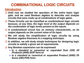
  • 1. COMBINATIONAL LOGIC CIRCUITS COMBINATIONAL LOGIC CIRCUITS Introduction ‰ Until now we studied the operation of the entire basic logic gate, and we used Boolean algebra to describe and analyze circuits that were made up of combinations of logic gates. ‰ These Circuits can be classified as combinational logic circuits because, at any time, the logic level at the output depends on the combination of logic levels present at the inputs. ‰ A combinational circuit has no memory characteristic, so its output depends on the current value of its input. ‰ We will study the simplification of logic circuits by using Boolean algebra theorems & a mapping technique. ‰ In addition, we will study simple techniques for designing logic circuits to satisfy a given set of requirements. ‰ Any Boolean expression can be expressed ¾ In a standard or canonical or expanded Sum (OR) Of Products (AND)-SOP form-or ¾ In a standard or canonical or expanded Product (AND) Of Sums (OR)-POS form.
  • 2. Sum Sum- - of of- - Products Form (Minterms) Products Form (Minterms) ‰ The methods of logic- circuit simplification and design that we will study require logic expression to be in a sum- of- products form (SOP SOP). ‰ Some examples of this form are: ‰ Each of this sum- of- product expression consists of two or more AND terms (products) that are ORed together. ‰ Each AND term consists of one or more variables appearing in either complemented or Uncomplemented form. ‰ Note that in a sum- of- products expression; one inversion sign can not cover more than one variable in a term. ‰ Example : we can not have C B A ABC + D D C C B A AB + + + GH EF D C B A + + + 1. 2. 3. T RS or ABC
  • 3. Product Product- - of of- - Sums (Maxterms Sums (Maxterms) ) ‰ There is another general form for logic expressions that is sometimes used in logic- circuit design. ‰ It is called the Product- of- sums form (POS POS), and it consists of two or more OR terms (sums) that are ANDed together. ‰ Each OR term contains one or more variables in complemented or Uncomplemented form. Here are some product- of- sums expressions; ‰ The methods of circuit simplification and design, which we will be using, are based on the sum- of- products form, so we will not be doing much with the products- of- sum form. ‰ It will, however, occur from time to time in some logic circuits, which have a particular structure. ) C A ( ) C B A ( + + + F ) D C ( ) B A ( + + 1. 2.
  • 4. CONVERSION FROM SOP to POS CONVERSION FROM SOP to POS and vice and vice- -versa versa ‰ A standard SOP form can always be converted to a standard POS form, by treating missing minterms of the SOP form as the maxterms of the POS form. ‰ Similarly, a standard POS form can always be converted to a standard SOP form, by treating the missing maxterms of the POS form as the minterms of the corresponding SOP form.
  • 5. EXPANSION OF A BOOLEAN EXPRESSION TO SOP FORM EXPANSION OF A BOOLEAN EXPRESSION TO SOP FORM ‰ The following steps are followed for the expansion of a Boolean expression in SOP form in standard SOP form: 1. Write down all the terms. 2. If one or more variables are missing in any term, expand that term by multiplying it with the sum of each one of the missing variable and its complement 3. Drop out the redundant terms ‰ Also, the given expression can be directly written in terms of its minterms by using the following procedure: 1. Write down all the terms. 2. Put Xs in terms where variables must be inserted to form a minterm. 3. Replace the non-complemented variables by 1s and the complemented variables by 0s, and use all combinations of Xs in terms of 0s and 1s to generate minterms. 4. Drop out all the redundant terms.
  • 6. Example#1 Expand to minterms and maxterms Solution ‰ The given expression is a two-variable function. ‰ In the first term , the variable B is missing; so, multiply it by . ‰ In the second term , the variable A is missing; so, multiply by . ‰ Therefore, ‰ The minterm m3 is missing in the SOP form. ‰ Therefore, the maxterm M3 will be present in the POS form. ‰ Hence the POS form is M3 i.e. . B A + B B + B ) A (A + ) A (A B ) B (B A B A + + + = + A B A + B A B A B A B A + + + = B A B A B A + + = 10 00 01 + + = 2 0 1 m m m + + = ∑ = m(0,1,2)
  • 8. Exercise 9 Expand to minterms and maxterms ABC C B A + +
  • 9. EXPANSION OF A BOOLEAN EXPRESSION TO POS FORM EXPANSION OF A BOOLEAN EXPRESSION TO POS FORM ‰ The expansion of a Boolean expression to the standard POS form is conducted as follows: 1. If one or more variables are missing in any sum term, expand that term by adding the products of each of the missing term and its complement. 2. Drop out the redundant terms. ‰ The given expression can also be written in terms of maxterms by using the following procedure: 1. Put Xs in terms wherever variables must be inserted to form a maxterm. 2. Replace the complemented variables by 1 s and the non-complemented variables by Os and use all combinations of Xs in terms of Os and 1 s to generate maxterms. 3. Drop out the redundant terms.
  • 10. Example#2 Expand to maxterms and minterms Solution ‰ The given expression is a two-variable function in the POS form. ‰ The variable B is missing In the first term A. so, add to it. ‰ The second term contains all the variables. So leave it as it is. ‰ The variable A is missing in the third term B. So, add to it. ‰ Therefore, or ‰ The maxterm M3 is missing in the POS form. So, the SOP form will contain only the minterm m3 i.e. AB A)B B A( + B B A A ) A A)(B (B A A B B ) B B)(A (A B B A A + + = + = + + = + = B) A B)( )(A B )(A B B)(A (A A)B B A( + + + + + = + B) A )( B B)(A (A + + + = (10) (01) (00) = 2 1 0 M M M ⋅ ⋅ = ∏ = M(0,1,2)
  • 12. Exercise 9 Expand to maxterms and minterms ) C B )(A C A A( + + + ) C B A )( C B A ( ) C B A )( C B A ( ) C C B A )( C C B A ( C C ) B A )( B A ( C C B B A A + + + + + + + + + = + + + + = + + + = + + = ) B C A )( B C A ( B B C A C A + + + + = + + = +
  • 13. SIMPLIFYING LOGIC CIRCUITS SIMPLIFYING LOGIC CIRCUITS Why simplification? Why simplification? ‰ Once the expression for a logic circuit has been obtained, we may be able to reduce it to a simpler form containing fewer terms of fewer variables in one or more terms. ‰ The new expression can then be used to implement a circuit that is equivalent to the original circuit but that contains fewer gates and connections. ‰ To illustrate, the circuit of fig (a) can be simplified to produce the circuit of fig (b). ‰ Since both circuits perform the same logic, it should be obvious that the simplest circuit is more desirable because it contains fewer gates and will therefore be smaller and cheaper than the original. ‰ Furthermore, the circuit reliability will improve because there are fewer interconnections that can be potential circuit faults. In subsequent sections we will study two methods for simplifying logic circuits: ¾ One method will utilize the Boolean algebra theorems (Algebraic Method Algebraic Method) and ¾ The other method will utilize Karnaugh mapping (K-map Method) ( ) ( ) B A C B A Y ⋅ ⋅ ⋅ + = C) (B A ⋅ + C B⋅ (a) unsimplified circuit A B A Y ⋅ = (b) Simplified circuit
  • 14. ALGEBRAIC SIMPLIFICATION ALGEBRAIC SIMPLIFICATION ‰ The Boolean algebra theorems that we studied earlier can be used to help us simplify the expression for logic circuit. ‰ Unfortunately, it is not always obvious which theorems should be applied in order to produce the simplest result. ‰ Furthermore, there is no easy way to tell whether the simplified expression is in its simplest form or whether it could have been simplified further. ‰ Thus, algebraic simplification often becomes a process of trial and error a process of trial and error. With experience, however, one can become adept at obtaining reasonably good results. ‰ The examples that follow will illustrate many of the ways in which the Boolean theorems can be applied in trying to simplify an expression. ‰ You should notice that these examples contain two essential steps; 1. The original expression is put in to the sum- of- products form by repeated application of De Morgan’s theorems and multiplication of terms. 2. Once it is in this form the product terms are checked for common factors, and factoring is performed wherever possible. Hopefully, the factoring results in the elimination of one or more terms.
  • 15. Example # 1 Example # 1 Simplify the expression 9 It is usually a good idea to break down all large inverter signs using De Morgan’s theorems and then multiply out all terms 9 With the expression now in sum-of-products form, we should look for common factors. ∴The first and third terms above have AC in common, which can be factored out: ) C A ( B A ABC Z + = ) C A ( B A ABC Z + + = C) (A B A ABC + + = C B A A B A ABC + + = C B A B A ABC + + = [multiply out] [theorem (19)] [cancel double inversions] [A.A=A] ] 1 B B [ = + B A ) B AC(B Z + + = B A AC(1) Z + = [factor out A] ) B A(C Z + = B A AC Z + =
  • 16. Example # 2 Example # 2 9 Simplify the expression Solution: 9 We will look at two different ways to arrive at the same result. Method 1 Method 1: : 9 The first two terms have the product AB in common. Thus, 9 We can factor the variable A from both terms 9 Invoking theorem (15), Method 2: 9 The first two terms have AB in common. 9 The first and the last terms have AC in common. 9 How do we know whether to factor AB from the first two terms or AC from the two-end terms? 9 Actually we can do both by using the ABC term twice. 9 In other words, we can rewrite the expression as 9 The extra term ABC is valid and will not change the value of the expression, Since ABC +ABC = ABC [Theorem(7)] 9 This is the same result as method 1. 9 In fact, the same term can be used more than twice if necessary. C B A C AB ABC Z + + = C B A ) C AB(C Z + + = C B A AB(1) + = C B A AB + = C) B A(B Z + = C) A(B Z + = ABC C B A C AB ABC Z + + + = B) B AC( C AB(C Z + + + = ) 1 AC 1 AB ⋅ + ⋅ = C) A(B + =
  • 17. Design procedures of combinational logic circuit using algebraic method STEP 1 :Set up the truth table STEP 2 :Write the AND term for each case where the output is a 1 STEP 3 :Write the SOP expression for the output STEP 4 :Simplify the output expression STEP 5 :Implement the circuit for the final expression
  • 18. Example #1. Design a logic circuit that has three inputs, A, B and C whose output will be high only when a majority of the inputs are high. Solution: Step 1 :Set up the truth table BC A C B A C AB ABC A B C X 0 0 0 0 0 0 1 0 0 1 0 0 0 1 1 1 1 0 0 0 1 0 1 1 1 1 0 1 1 1 1 1 STEP 2
  • 19. Step 3 Step 3. Write the Sum Write the Sum- -of of- -products expression for the output. products expression for the output. Step 4. ABC C AB C B A BC A X + + + = Step 4. Simplify the output expression. Simplify the output expression. 9 9 This expression can be simplified in several ways. This expression can be simplified in several ways. 9 9 Perhaps the quickest way is to realize that the last term ABC tw Perhaps the quickest way is to realize that the last term ABC two o variables in common with each of the other terms. variables in common with each of the other terms. 9 9 Factoring the appropriate pairs of terms , we have Factoring the appropriate pairs of terms , we have 9 9 Since each term in the parenthesis is equal to 1, we have ABC C AB ABC C B A ABC BC A X + + + + + = C) C AB( B) B AC( A) A BC( X + + + + + = Since each term in the parenthesis is equal to 1, we have AB AC BC X + + =
  • 20. Step 5. Step 5. Implement the circuit for the final expression. Implement the circuit for the final expression. 9 9 The The X= AB + BC + AC X= AB + BC + AC expression is implemented in fig. below. expression is implemented in fig. below. 9 9 Since the expression is in SOP, the circuit consists of a group Since the expression is in SOP, the circuit consists of a group of of AND gates working into a single OR gate. AND gates working into a single OR gate. AB AB BC BC AC AC X = AB+ BC + AC X = AB+ BC + AC
  • 21. Example # 2 Example # 2: 9 refer to fig (a), where four logic-signal lines A, B, C, D are being used to represent a 4-bit binary number with A as the MSB and D as the LSB. The binary inputs are fed to a logic circuit that produces a HIGH output only when the binary number is greater than 01102 = 610 . 9 Design this circuit Fig.(a)
  • 22. TRUTH TABLE A B C D Z 8 1 0 0 0 9 1 0 0 1 10 1 0 1 0 11 1 0 1 1 12 1 1 0 0 13 1 1 0 1 14 1 1 1 0 15 1 1 1 1 A B C D Z 0 0 0 0 0 1 0 0 0 1 2 0 0 1 0 3 0 0 1 1 4 0 1 0 0 5 0 1 0 1 6 0 1 1 0 7 0 1 1 1
  • 23. STEP:2 STEP:2 A B C D Z 8 1 0 0 0 1 9 1 0 0 1 1 10 1 0 1 0 1 11 1 0 1 1 1 12 1 1 0 0 1 13 1 1 0 1 1 14 1 1 1 0 1 15 1 1 1 1 1 A B C D Z 0 0 0 0 0 0 1 0 0 0 1 0 2 0 0 1 0 0 3 0 0 1 1 0 4 0 1 0 0 0 5 0 1 0 1 0 6 0 1 1 0 0 7 0 1 1 1 1 D C B A D C B A D C B A CD B A D C AB D C AB D ABC ABCD BCD A
  • 24. Step 3 Step 3. SOP expression SOP expression ABCD D ABC D C AB D C AB CD B A D C B A D C B A D C B A BCD + + + + + + + + = A Z Step:4 Step:4 Simplification Simplification ABCD D ABC D C AB D C AB CD B A D C B A D C B A D C B A BCD + + + + + + + + = A Z ) D D ( ABC ) D D ( C AB ) D D ( C B A ) D D ( C B A BCD A Z + + + + + + + + = ABC C AB C B A C B A BCD A + + + + = ) C C ( AB ) C C ( B A BCD A + + + + = AB B A BCD A + + = ) B B ( A BCD A + + = A BCD A + = A BCD Z + =
  • 25. AOI LOGIC CIRCUIT AOI LOGIC CIRCUIT (for example # 1) (for example # 1)
  • 26.
  • 28. NAND/NAND LOGIC CIRCUIT NAND/NAND LOGIC CIRCUIT AB BC AC AC BC AB X ⋅ ⋅ =
  • 29. AOI LOGIC CIRCUIT AOI LOGIC CIRCUIT (for example # 2) (for example # 2)
  • 30. 9 9 We can streamline the process of converting a sum We can streamline the process of converting a sum- -of of- - products circuit from AND/OR to NAND gates as follows: products circuit from AND/OR to NAND gates as follows: 1. 1. Replace each AND gate, OR gate, and Inverter by a single Replace each AND gate, OR gate, and Inverter by a single NAND gate. NAND gate. 2. 2. Use a NAND gate to invert any single variable that is feeding Use a NAND gate to invert any single variable that is feeding the final OR gate. the final OR gate. AOI LOGIC CIRCUIT AOI LOGIC CIRCUIT NAND/NAND LOGIC CIRCUIT NAND/NAND LOGIC CIRCUIT BCD A Y ⋅ = BCD A