ELECTRON MICROSCOPY (TEM & SEM)
•Download as PPTX, PDF•
11 likes•2,254 views

ELECTRON MICROSCOPY TRANSMISSION ELECTRON MICROSCOPY SCANING ELECTRON MICROSCOPY

Recommended
Recommended
More Related Content
What's hot
What's hot (20)
Similar to ELECTRON MICROSCOPY (TEM & SEM)
Similar to ELECTRON MICROSCOPY (TEM & SEM) (20)
More from ADITYA ARYA
More from ADITYA ARYA (20)
Recently uploaded
Recently uploaded (20)
ELECTRON MICROSCOPY (TEM & SEM)
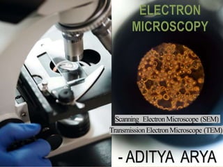
- 1. - ADITYA ARYA Scanning ElectronMicroscope (SEM) TransmissionElectronMicroscope (TEM)
- 2. Electron Microscopy • Electron microscopes are scientific instruments that use a beam of energetic to examine objects on a very fine scale. • Electron microscopes use beam of electron in place of light • Object cannot be perceived by our eyes directly. • The image produced by electron microscopes is perceived by CRT or X- ray plates. • Electron microscopes were developed due to the limitations of light microscopes which are limited by the physics of light. • In the early 1930’s this theoretical limit had been reached and there wasa scientific desire to see the fines details of the interior structure of organic cells (nucleus, mitochondria, etc.) • This required 10,000x plus magnification which wasnot possible using current optical microscopes.
- 3. Electron microscope constructed by Ernst Ruska in1933 Amodern transmission electron microscope
- 4. Summary of Electron Microscopes components 1. Electron optical column consist of: -Electron source to produce electrons -magnetic lenses to de-magnify the beam -magnetic coils to control and modify the beam - aperture to define the beam, prevent electron spray, etc. 2. Vaccum systems consists of: - Chamber which “holds” vaccum, pumps to produce vaccum - valves to control vaccum, gauges to moniter vaccum. 3. Signaldetection &displayconsists of: -Detectors which collect the signal -electronics which produce an image from the signal
- 5. Different types of Electron Microscopy 1. Scanning Electron Microscope (SEM) 2. Transmission Electron Microscope (TEM) 3. Scanning Transmission Electron Microscope (STEM) 4. Modern Methods of Atomic level microscopy – - Field Ion Microscope - Scanning Probe Microcopy
- 6. Scanning Electron Microscope (SEM) INTRODUCTION :- -It provides a valuable combination of high resolution imaging, elemental analysis, and recently, crystallographic analysis. -It is used for inspecting topographies of specimens at very high magnifications using a piece of equipment called the scanning electron microscope. -SEM magnifications can go to more than 300,000 X but most semiconductor manufacturing applications require magnifications of less than 3,000 X only. -It is often used in the analysis of die/package cracks and fracture surfaces, bond failures, and physical defects on the die or package surface. -Identifying crystalline compounds and determining crystallographic orientations of microstructural features as small as 1 µm (recently developed capability--not currently widely used, but likely to become so).
- 7. M. von Ardenne's first SEM Analog type SEM SEM opened sample chamber
- 8. Image of pollen grains taken on an SEM shows the characteristic depth of field of SEM micrographs.
- 9. Working of Scanning Electron Microscope
- 10. Working Principle •The main components of a typical SEM are electron column, scanning system, detector(s), display, vacuum system and electronics controls in figure. •The electron column consists of an electron gun and two or more Electromagnetic lenses operating in vacuum. •The electron gun generates free electrons & accelerates these electrons to energies in the range 1-40 keV in the SEM. • Purpose of the electron lenses is to create a small, focused electron probe on the Specimen. •Most SEMs can generate an electron beam at the specimen surface with spot Size less than 10 nm. •Max. size of specimen can used upto 2.5 X 10^-7 nm.
- 11. • In order to produce images the electron beam is focused into a fine probe. • Its scanned across the surface of the specimen with the help of scanning coils (Fig. on the previous slide). • With a higher accelerating voltage the electronbeam penetration is greater and the interaction volume is larger. • Therefore, the spatial resolution of micrographs created from those signals will be reduced. • So there will be a brighter image because the no. of backscattered electrons (BSEs) willincrease but the resolution willbeworse. • For secondary electron (SE) imaging at typical voltages (say 15 keV),BSEs can enter the secondary electron detector and degrade resolution because they come from deeper in the sample. • Complex interactions of the beam electrons with the atoms of the specimen produce wide variety of radiation. • In such case knowledge of electron optics, beam-specimen interactions, detection, and visualization processes is necessary for successful utilization of the power of the SEM.
- 12. Components of SEM 1. Electron Column: • The electron column is where the electron beam is generated under vacuum (Fig. 11). • Focused to a small diameter, and scanned across the surface of a specimen by electromagnetic deflection coils. • The lower portion of the column is called the specimen chamber. • The secondary electron detector is located above the sample stage inside the specimen chamber. • Specimens are mounted and secured onto the stage which is controlled by a goniometer. • The manual stage controls are found on specimen chamber and allow for x-y-zmovement, 360 rotation and 90 tilt (Fig. given below).
- 13. • It located at the top of the column. • Free electrons are generated by thermionic emission from a tungsten filament at ~2700K. • The filament is inside the Wehnelt which controls the number of electrons leaving the gun. • Electrons are primarily accelerated toward an anode that is adjustable from 200V to 30 kV(1kV=1000V) as shown in Fig. 12. A. Electron Gun :
- 15. MajorElectron Beam Parameters •Four electron beam parameters define the probe which determine resolution, contrast, and depth of focus of SEM images: Probe diameter – dp Probe current – Ip Probe convergence angle – αp Accelerating Voltage – Vo •These interdependent parameters must be balanced by the operator to optimize the probe conditions depending on needs: Resolution Depth of Focus Image Quality (S/N ratio) Analytical Performance Electron optical brightness, β, is a constant throughout the column, thus is a very important electron source parameter [13] -
- 16. Secondary Electron Yield :
- 18. •After the beam passes the anode it is influenced by two condenser lenses that cause the beam to converge and pass through a focal point (Fig. 13). •The electron beam is essentially focused down to 1000 times its original size. •It is responsible for determining the intensity of the electron beam when it strikes the specimen [10]. (1/u)+ (1/v)= (1/f) M =v/ u B. Condenser Lenses:
- 19. • Depending on microscope one or more apertures may be found. •The function of apertures is to reduce and exclude extraneous electrons in the lenses. •The final lens aperture located below the scanning coils determines the dia. or spot size of the beam at the specimen. •It willin partlydetermine the resolution and depth of field. • Decreasing the spot size will allow for an increase in resolution and depth of field with a loss of brightness [10]. C. Apertures: Aperture diffraction causes a fundamental limit to the achievable probe size
- 20. •Images are formed by rastering the electron beam across the specimen using deflection coils inside the objective lens. •The stigmatoror astigmatism corrector is located in the objective lens. • Uses of a magnetic field in order to reduce aberrationsof the electron beam. •Beam should have a circular cross section when it strikes the specimen [10,11]. •Contrast from predominately angular dependence of secondary electron yield and edge effects. D. ScanningSystem:
- 22. • At the lower portion of the column the specimen stage and controls are located. •The secondary electrons from the specimen are attracted to the detector by a positive charge. E. Specimen Chamber:
- 23. 2. Vaccum System : • To provide a controlled electron beam requires column be under vacuum at a pressure of at least 5x10^-5 Torr. • A high vacuum pressure is required for a variety of reasons. • First, the current that passes throughthe filament reach temperatures around 2700K [12]. • Afilament willoxidize and burnout in the presence of air at atmospheric pressure. • Secondly, the column optics to operate properly requires a fairly clean, dust-free environment. • Third, air particles and dust inside the column can interfere and block the electrons [10]. •In order to provide adequate vacuumpressure inside the column, a vacuum system consisting of two or more pumps is typically present.
- 24. 3. Electron Beam-Specimen Interactions •To achieve higher resolutions, an electron source is required instead of light as the illumination source. • Which allows for resolutions of about 25 Angstroms. •The use of electrons not only gives better resolution but, due to the nature electron beam specimen interactions there are a variety of signals •That can be used to provide information regarding characteristics at and near the surface of a specimen.
- 26. Some Common Errors & Images of SEM 1. Image Disturbances 2. Effect of Accelerating Voltage 3. Effect of Working Distance 4. Effect of Spot Size
- 27. a) ZnO Nano wires
- 29. Advantages & Disadvantages Advantages • High resolution &Depth of focus (1 X 10^-6 nm) • Elemental analysis attachments • Almost all kinds of samples, conducting and non-conducting (stain coating needed) • Based on surface interaction ---no requirement of electron-transparentsample • Imaging at all directions through x-y-z(3D) rotation of sample. Disadvantages * Cost * More knobs * Vacuum * Low resolution, usually above a fewtens of nanometers. * Usually required surface stain-coating with metals for electron conducting.
- 30. Transmission Electron Microscope (TEM) INTRODUCTION :- • In it a beam of highly focused electrons are directed toward a thinned sample (<200 nm). • Normally no scanning required ---helps the high resolution, compared to SEM. • These highly energetic incident electrons interact with the atoms in the sample producing characteristic radiation • And particles providing information for materials characterization. •Information is obtained from both deflected and non-deflected transmitted electrons, backscattered and secondary electrons, andemitted photons.
- 32. The first practical TEM, originally installed at IG Farben -Werke and now on display at the Deutsches Museum in Munich, Germany
- 33. A TEM image of a cluster of poliovirus. The polio virus is 30 nm in diameter.
- 34. • Lower resolution/large area techniques should be first performed to get a ‘broad picture’ about the sample. • This includes XRD and SEM. We can even start with optical microscopy. • Phase related information should be obtained via XRD. •Chemical information viaEDX in SEM should also be obtained (any chemical in homogeneity should be noted). • On ‘usual’ samples conventional TEM should be performed before trying out HRTEM. Sampling on aTEM?
- 35. • The wavelength of the electrons in a 10 kV SEM is 12.3 x10⁻¹² m (12.3 pm) • In a 200 kV TEM the wavelength is 2.5 pm • Wavelength of X-rays usually used in XRD is in the order of 100 pm (Cu kα: λ=154 pm). Operating conditions ofTEM Instrument Operating Voltage λX-rayor λElectron X-rays - 1.54 Å SEM 10 kV 0.12 Å TEM 200 kV 0.02 Å
- 36. • The sample is a thin 3mm disc. The central portion of the disc is thinned down further to make it electron transparent (<1000 Å in thickness). • The process of sample preparation usually leaves a hole(s) in the ‘middle’ with electron transparent region next it. • The thin regions in the sample can bend. • The standard image seen on the screen or captured in the camera isa projected image integrated through the thickness. The TEM sample & the projectedimage :
- 37. Atransmission Electron Microscope is anologous to a slide projector as indicated by Philips above. Introduction toTEM The first transmission electron microscope wasinvented in 1933 by Max Knoll and Ernst Ruska at the Technical College in Berlin.
- 38. Instrument components - Electron gun - Condenser system (lenses &apertures for controlling illumination on specimen) - Specimen chamberassembly. - Objective lens system A. image -forming lens -limits resolution; B.Aperture -controls imaging conditions -Projectorlens system (magnifies image or diffraction pattern onto final screen)
- 39. Working : 1.In a conventional transmissionelectron microscope, a thin specimen is irradiated with an electron beam of uniform current density. 2.Electrons are emitted from the electron gun and illuminate the specimen through a two or three stage condenser lenssystem. 3.Objective lens provides the formationof either image or diffraction pattern of the specimen. 4.The electron intensity distribution behind the specimen is magnified with a three or four stage lens system and viewed on a fluorescent screen. Working Principles
- 41. Examples :
- 42. • TEM provides information of: - Structural - Chemical • Modes -Imaging -Diffraction 1. In TEM wecan switch from an image (Real Space) to diffraction (reciprocal space) by the switch of a button. 2. We can get spectroscopic information and use it for forming an image or diffraction patterns. TEM Facility
- 43. TEM components 1. Electron gun : • At the top of the column, the electron gun delivers high-energy electrons to the instrument. • Thermionic guns (tungsten or LaB6) are the most common types. • The appropriate electron energy depends on the nature of the specimen and the kind of information required. • Higher electron energies allow thicker samples to be analysed and, due to their smaller wavelengths, increase the resolution possible; • however, it is rare now to see TEMs which operate at energies greater than 200 keV. • The introduction of field emission guns and improvements in lens design have largely made higher-energy microscopes unnecessary for high-resolution. • Additionally, higher energy electrons cause increasing amounts of damage to samples. Biological samples in particular require lower operating voltages.
- 44. •TEM images are simply magnified images of the electron intensity on the bottom surface of the specimen and contrast arises only if the intensity varies significantly from one region to another. 1. Absorption contrast • Examination of samples which are thicker, denser, or with higher atomic number allow fewer electrons to pass through • It applies to both amorphous and crystalline specimens and is used extensively by biologists who call it mass-thickness. • In crystalline samples, this contrast mechanism is usually swamped by others. 2. Diffraction Contrast • Diffraction contrast is simply a function of the diffraction conditions. • It is the method most commonly used to study crystal defects like dislocations, stacking faults, precipitates, etc. •It is the mechanism which explains extinction (bend) contours and thickness fringes. Image Contrast in the TEM:
- 48. • We see something if: (i) Light (visible part of the spectrum) enter our eyes, (ii)the light has sufficient intensity, (iii)There is sufficient contrast in the image. •Contrast is a dimensionless number as defined below. It is to be noted that contrast is not the difference in intensity between the light (I1) and dark (I2) regions, but the difference divided by the (say) higher of the two intensities (I2). • Acontrast value of 5-10%can be picked discerned by our eyes. • We have strong or weak contrast* (but not bright or dark contrast).
- 49. 1. Amplitude Contrast • Diffraction contrast (Coherent elastic scattering ) - Bright Field &Dark Field Images • Absorption contrast (In-coherent elastic scattering ) - Mass-thickness contrast → small effect in a thin specimen 2. Phase contrast • Thickness Fringes • Bend Contours • Fresnel Fringes • Moiré Patterns -Beats is the time analogue of Moiré patterns • Phase contrast • Lattice Fringes Contrast are of twotypes
- 54. Phase contrastand high - resolution imaging •Unlike absorption and diffraction contrast mechanisms, which rely on the amplitude of scattered waves, phase contrast results whenever electrons of a different phase pass through the objective aperture . • If spots along a systematic row are allowed through, a latticeimageis formed . •Such images can be used to show the extent of crystallisation of a grain -boundary film or the habit plane of planar defects . •If more diffracted beams are allowed to contribute, then a structureimagecan be formed .
- 55. Resolution • Resolution of human eyes ~ (0.1 –0.2) mm. • Highest useful magnification is governed by the resolution. • Raleigh criterion is used for the definition of resolution. • Optical Microscope; • δ= 0.61λ/μsinβ (Green light λ=550nm, δ=300nm, 1000 atomic diameter) • δ= λ/2, δ → Smallest distance that can be resolved, λ → Wavelength of radiation β → Semi-angle of collection & μ → Refractive index of viewing medium • TEM λ ~ 1.22/√E (Eλ100keV electrons → λ =4 pm ) • Aspects determining the resolution – 1.Wavelength of the radiation 2. Aberration of the lenses in the imaging system 3. Diffraction limit of the imaging system
- 56. Requirement of interpretableimages 1. Very thin (about 5nm) specimens. If they are too thick, inelastic scattering degrades the phase contrast information. 2. To be at a zone axis so that many beams are available and the crystallographic information is interpretable. 3. Only those diffracted beams which correspond to distances within the point resolution of the HREM willcontribute to the image. 4. Precise alignment of the electron beam down the optic axis.Also, any defects must lie along the beam direction. 5. Coherent illumination (i.e., LaB6 filament or FEG). 6.Aspecific value of objective defocus. In order to establish this value, the quantitative defocus associated with each “click” of the objective focus control must be calibrated 7. As the image obtained is a function of a number of variables, these must be defined and calibrated in order to interpret the image. a. Sample thickness b. Objective lens defocus c. Microscope parameters like kV, Cs, Cc, etc. d. Number and type of beams included in the objective aperture. e. Beam tilt
- 57. Advantages & Disadvantages Advantages • High resolution, as small as 0.2 nm. • Direct imaging of crystalline lattice. • Delineate the defects inside the sample. • No metallic stain-coating needed, thus convenient for structural imaging of organic materials, • Electron diffraction technique: phase identification, structure and symmetry determination, lattice parameter measurement, disorder and defect identification. Disadvantages • Low sampling volume and rather slow process of obtaining information. • High capital and running cost. • Special training required for the operation of the equipment. • Difficult sample preparation. Possibility of electron beam damage. • Samples which are not stable in vacuum are difficult to study. • Magnetic samples require special care. • Non-conducting samples require gold or carbon coating. • Difficulty in the interpretation of images. In usual mode of operation information is integrated along the beam direction.
- 58. References : 1. http://www.youtube.com/watch?annotation_id=annotation_100990&feat ure=iv&src_vid=L6d3zD2LtSI&v=ntPjuUMdXbg(I) 2.http://www.youtube.com/watch?v=VQtMHj3vaLg(II)Partsand Functionof aMicroscope(details) 3.Doug,Holly& Oleg,“SEM Microscope”. 4.All theremainingfiguresaretakenfromgoogle.comwebsite. 5.Scanning ElectronMicroscopy:Physics ofImageFormationandMicro analysis(SpringerSeries in OpticalSciences) byLudwigReimerand P.W.Hawkes (Hardcover-Oct16,1998). 6.A GuidetoX-Ray Microanalysis,OxfordMicroanalyticalInstruments. 7.A TransmissionElectronMicroscopeis anologoustoaslide projectoras indicatedbyPhilips. 8.ImageReferences: WIKIPEDIA