
Recommended
More Related Content
What's hot
What's hot (19)
Similar to Original Logic IC SN74LVC14A SN54LVC14A 74LVC14A 54LVC14A SOP-14 New Texas Instruments
Similar to Original Logic IC SN74LVC14A SN54LVC14A 74LVC14A 54LVC14A SOP-14 New Texas Instruments (20)
More from AUTHELECTRONIC
More from AUTHELECTRONIC (20)
Recently uploaded
Recently uploaded (20)
Original Logic IC SN74LVC14A SN54LVC14A 74LVC14A 54LVC14A SOP-14 New Texas Instruments
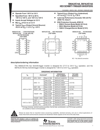
- 1. SN54LVC14A, SN74LVC14A HEX SCHMITTĆTRIGGER INVERTERS SCAS285W − MARCH 1993 − REVISED FEBRUARY 2004 1POST OFFICE BOX 655303 • DALLAS, TEXAS 75265 D Operate From 1.65 V to 3.6 V D Specified From −40°C to 85°C, −40°C to 125°C, and −55°C to 125°C D Inputs Accept Voltages to 5.5 V D Max tpd of 6.4 ns at 3.3 V D Typical VOLP (Output Ground Bounce) <0.8 V at VCC = 3.3 V, TA = 25°C D Typical VOHV (Output VOH Undershoot) >2 V at VCC = 3.3 V, TA = 25°C D Latch-Up Performance Exceeds 100 mA Per JESD 78, Class II D ESD Protection Exceeds JESD 22 − 2000-V Human-Body Model (A114-A) − 200-V Machine Model (A115-A) − 1000-V Charged-Device Model (C101) SN74LVC14A . . . RGY PACKAGE (TOP VIEW) 1 14 7 8 2 3 4 5 6 13 12 11 10 9 6A 6Y 5A 5Y 4A 1Y 2A 2Y 3A 3Y 1A 4YV GND CC 1 2 3 4 5 6 7 14 13 12 11 10 9 8 1A 1Y 2A 2Y 3A 3Y GND VCC 6A 6Y 5A 5Y 4A 4Y SN54LVC14A . . . J OR W PACKAGE SN74LVC14A . . . D, DB, DGV, NS, OR PW PACKAGE (TOP VIEW) 3 2 1 20 19 9 10 11 12 13 4 5 6 7 8 18 17 16 15 14 6Y NC 5A NC 5Y 2A NC 2Y NC 3A 1Y 1A NC 4Y 4A V 6A 3Y GND NC SN54LVC14A . . . FK PACKAGE (TOP VIEW) CC NC − No internal connection description/ordering information The SN54LVC14A hex Schmitt-trigger inverter is designed for 2.7-V to 3.6-V VCC operation, and the SN74LVC14A hex Schmitt-trigger inverter is designed for 1.65-V to 3.6-V VCC operation. ORDERING INFORMATION TA PACKAGE† ORDERABLE PART NUMBER TOP-SIDE MARKING −40°C to 85°C QFN − RGY Reel of 1000 SN74LVC14ARGYR LC14A Tube of 50 SN74LVC14AD SOIC − D Reel of 2500 SN74LVC14ADR LVC14ASOIC − D Reel of 250 SN74LVC14ADT LVC14A SOP − NS Reel of 2000 SN74LVC14ANSR LVC14A −40°C to 125°C SSOP − DB Reel of 2000 SN74LVC14ADBR LC14A−40 C to 125 C Tube of 90 SN74LVC14APW TSSOP − PW Reel of 2000 SN74LVC14APWR LC14ATSSOP − PW Reel of 250 SN74LVC14APWT LC14A TVSOP − DGV Reel of 2000 SN74LVC14ADGVR LC14A CDIP − J Tube of 25 SNJ54LVC14AJ SNJ54LVC14AJ −55°C to 125°C CFP − W Tube of 150 SNJ54LVC14AW SNJ54LVC14AW−55 C to 125 C LCCC − FK Tube of 55 SNJ54LVC14AFK SNJ54LVC14AFK † Package drawings, standard packing quantities, thermal data, symbolization, and PCB design guidelines are available at www.ti.com/sc/package. Copyright 2004, Texas Instruments IncorporatedPRODUCTION DATA information is current as of publication date. Products conform to specifications per the terms of Texas Instruments standard warranty. Production processing does not necessarily include testing of all parameters. Please be aware that an important notice concerning availability, standard warranty, and use in critical applications of Texas Instruments semiconductor products and disclaimers thereto appears at the end of this data sheet. On products compliant to MILĆPRFĆ38535, all parameters are tested unless otherwise noted. On all other products, production processing does not necessarily include testing of all parameters.
- 2. SN54LVC14A, SN74LVC14A HEX SCHMITTĆTRIGGER INVERTERS SCAS285W − MARCH 1993 − REVISED FEBRUARY 2004 2 POST OFFICE BOX 655303 • DALLAS, TEXAS 75265 description/ordering information (continued) The devices contain six independent inverters and perform the Boolean function Y = A. Inputs can be driven from either 3.3-V or 5-V devices. This feature allows the use of these devices as translators in a mixed 3.3-V/5-V system environment. FUNCTION TABLE (each inverter) INPUT A OUTPUT Y H L L H logic diagram, each inverter (positive logic) YA absolute maximum ratings over operating free-air temperature range (unless otherwise noted)† Supply voltage range, VCC −0.5 V to 6.5 V. . . . . . . . . . . . . . . . . . . . . . . . . . . . . . . . . . . . . . . . . . . . . . . . . . . . . . . . . Input voltage range, VI (see Note 1) −0.5 V to 6.5 V. . . . . . . . . . . . . . . . . . . . . . . . . . . . . . . . . . . . . . . . . . . . . . . . . Output voltage range, VO (see Notes 1 and 2) −0.5 V to VCC + 0.5 V. . . . . . . . . . . . . . . . . . . . . . . . . . . . . . . . . . Input clamp current, IIK (VI < 0) −50 mA. . . . . . . . . . . . . . . . . . . . . . . . . . . . . . . . . . . . . . . . . . . . . . . . . . . . . . . . . . . Output clamp current, IOK (VO < 0) −50 mA. . . . . . . . . . . . . . . . . . . . . . . . . . . . . . . . . . . . . . . . . . . . . . . . . . . . . . . . Continuous output current, IO ±50 mA. . . . . . . . . . . . . . . . . . . . . . . . . . . . . . . . . . . . . . . . . . . . . . . . . . . . . . . . . . . . . Continuous current through VCC or GND ±100 mA. . . . . . . . . . . . . . . . . . . . . . . . . . . . . . . . . . . . . . . . . . . . . . . . . . Package thermal impedance, θJA (see Note 3): D package 86°C/W. . . . . . . . . . . . . . . . . . . . . . . . . . . . . . . . . . . (see Note 3): DB package 96°C/W. . . . . . . . . . . . . . . . . . . . . . . . . . . . . . . . . (see Note 3): DGV package 127°C/W. . . . . . . . . . . . . . . . . . . . . . . . . . . . . . . (see Note 3): NS package 76°C/W. . . . . . . . . . . . . . . . . . . . . . . . . . . . . . . . . (see Note 3): PW package 113°C/W. . . . . . . . . . . . . . . . . . . . . . . . . . . . . . . . (see Note 4): RGY package 47°C/W. . . . . . . . . . . . . . . . . . . . . . . . . . . . . . . . Storage temperature range, Tstg −65°C to 150°C. . . . . . . . . . . . . . . . . . . . . . . . . . . . . . . . . . . . . . . . . . . . . . . . . . . Power dissipation, Ptot (TA = −40°C to 125°C) (see Notes 5 and 6) 500 mW. . . . . . . . . . . . . . . . . . . . . . . . . . . . † Stresses beyond those listed under “absolute maximum ratings” may cause permanent damage to the device. These are stress ratings only, and functional operation of the device at these or any other conditions beyond those indicated under “recommended operating conditions” is not implied. Exposure to absolute-maximum-rated conditions for extended periods may affect device reliability. NOTES: 1. The input negative-voltage and output voltage ratings may be exceeded if the input and output current ratings are observed. 2. The value of VCC is provided in the recommended operating conditions table. 3. The package thermal impedance is calculated in accordance with JESD 51-7. 4. The package thermal impedance is calculated in accordance with JESD 51-5. 5. For the D package: above 70°C, the value of Ptot derates linearly with 8 mW/K. 6. For the DB, DGV, NS, and PW packages: above 60°C, the value of Ptot derates linearly with 5.5 mW/K.
- 3. SN54LVC14A, SN74LVC14A HEX SCHMITTĆTRIGGER INVERTERS SCAS285W − MARCH 1993 − REVISED FEBRUARY 2004 3POST OFFICE BOX 655303 • DALLAS, TEXAS 75265 recommended operating conditions (see Note 7) SN54LVC14A −55 TO 125°C UNIT MIN MAX UNIT VCC Supply voltage Operating 2 3.6 VVCC Supply voltage Data retention only 1.5 V VI Input voltage 0 5.5 V VO Output voltage 0 VCC V IOH High-level output current VCC = 2.7 V −12 mAIOH High-level output current VCC = 3 V −24 mA IOL Low-level output current VCC = 2.7 V 12 mAIOL Low-level output current VCC = 3 V 24 mA NOTE 7: All unused inputs of the device must be held at VCC or GND to ensure proper device operation. Refer to the TI application report, Implications of Slow or Floating CMOS Inputs, literature number SCBA004. recommended operating conditions (see Note 7) SN74LVC14A TA = 25°C −40 TO 85°C −40 TO 125°C UNIT MIN MAX MIN MAX MIN MAX UNIT VCC Supply voltage Operating 1.65 3.6 1.65 3.6 1.65 3.6 VVCC Supply voltage Data retention only 1.5 1.5 1.5 V VI Input voltage 0 5.5 0 5.5 0 5.5 V VO Output voltage 0 VCC 0 VCC 0 VCC V VCC = 1.65 V −4 −4 −4 IOH High-level output current VCC = 2.3 V −8 −8 −8 mAIOH High-level output current VCC = 2.7 V −12 −12 −12 mA VCC = 3 V −24 −24 −24 VCC = 1.65 V 4 4 4 IOL Low-level output current VCC = 2.3 V 8 8 8 mAIOL Low-level output current VCC = 2.7 V 12 12 12 mA VCC = 3 V 24 24 24 NOTE 7: All unused inputs of the device must be held at VCC or GND to ensure proper device operation. Refer to the TI application report, Implications of Slow or Floating CMOS Inputs, literature number SCBA004.
- 4. SN54LVC14A, SN74LVC14A HEX SCHMITTĆTRIGGER INVERTERS SCAS285W − MARCH 1993 − REVISED FEBRUARY 2004 4 POST OFFICE BOX 655303 • DALLAS, TEXAS 75265 electrical characteristics over recommended operating free-air temperature range (unless otherwise noted) SN54LVC14A PARAMETER TEST CONDITIONS VCC −55 TO 125°C UNITPARAMETER TEST CONDITIONS VCC MIN TYP MAX UNIT VT+ 2.7 V 0.8 2VT+ Positive-going threshold 3 V 0.9 2 VPositive-going threshold 3.6 V 1.1 2 V VT− 2.7 V 0.4 1.4VT− Negative-going threshold 3 V 0.6 1.5 VNegative-going threshold 3.6 V 0.8 1.7 V ∆VT 2.7 V 0.3 1.1∆VT Hysteresis (V − V ) 3 V 0.3 1.2 VHysteresis (VT+ − VT−) 3.6 V 0.3 1.2 V IOH = −100 µA 2.7 V to 3.6 V VCC−0.2 VOH IOH = −12 mA 2.7 V 2.2 VVOH IOH = −12 mA 3 V 2.4 V IOH = −24 mA 3 V 2.2 IOL = 100 µA 2.7 V to 3.6 V 0.2 VOL IOL = 12 mA 2.7 V 0.4 VVOL IOL = 24 mA 3 V 0.55 V II VI = 5.5 V or GND 3.6 V ±5 µA ICC VI = VCC or GND, IO = 0 3.6 V 10 µA ∆ICC One input at VCC − 0.6 V, Other inputs at VCC or GND 2.7 V to 3.6 V 500 µA Ci VI = VCC or GND 3.3 V 5† pF † TA = 25°C
- 5. SN54LVC14A, SN74LVC14A HEX SCHMITTĆTRIGGER INVERTERS SCAS285W − MARCH 1993 − REVISED FEBRUARY 2004 5POST OFFICE BOX 655303 • DALLAS, TEXAS 75265 electrical characteristics over recommended operating free-air temperature range (unless otherwise noted) SN74LVC14A PARAMETER TEST CONDITIONS VCC TA = 25°C −40 TO 85°C −40 TO 125°C UNITPARAMETER TEST CONDITIONS VCC MIN TYP MAX MIN MAX MIN MAX UNIT 1.65 V 0.4 1.3 0.4 1.3 0.4 1.3 1.95 V 0.6 1.5 0.6 1.5 0.6 1.5 VT+ 2.3 V 0.8 1.7 0.8 1.7 0.8 1.7VT+ Positive-going threshold 2.5 V 0.8 1.7 0.8 1.7 0.8 1.7 VPositive-going threshold 2.7 V 0.8 2 0.8 2 0.8 2 V 3 V 0.9 2 0.9 2 0.9 2 3.6 V 1.1 2 1.1 2 1.1 2 1.65 V 0.15 0.85 0.15 0.85 0.15 0.85 1.95 V 0.25 0.95 0.25 0.95 0.25 0.95 VT− 2.3 V 0.4 1.2 0.4 1.2 0.4 1.2VT− Negative-going threshold 2.5 V 0.4 1.2 0.4 1.2 0.4 1.2 VNegative-going threshold 2.7 V 0.4 1.4 0.4 1.4 0.4 1.4 V 3 V 0.6 1.5 0.6 1.5 0.6 1.5 3.6 V 0.8 1.7 0.8 1.7 0.8 1.7 1.65 V 0.1 1.15 0.1 1.15 0.1 1.15 1.95 V 0.15 1.25 0.15 1.25 0.15 1.25 ∆VT 2.3 V 0.25 1.3 0.25 1.3 0.25 1.3∆VT Hysteresis (V − V ) 2.5 V 0.25 1.3 0.25 1.3 0.25 1.3 VHysteresis (VT+ − VT−) 2.7 V 0.3 1.1 0.3 1.1 0.3 1.1 V T+ T− 3 V 0.3 1.2 0.3 1.2 0.3 1.2 3.6 V 0.3 1.2 0.3 1.2 0.3 1.2 IOH = −100 µA 1.65 V to 3.6 V VCC−0.2 VCC−0.2 VCC−0.3 IOH = −4 mA 1.65 V 1.29 1.2 1.05 VOH IOH = −8 mA 2.3 V 1.9 1.7 1.65 VVOH IOH = −12 mA 2.7 V 2.2 2.2 2.05 V IOH = −12 mA 3 V 2.4 2.4 2.25 IOH = −24 mA 3 V 2.3 2.2 2 IOL = 100 µA 1.65 V to 3.6 V 0.1 0.2 0.3 IOL = 4 mA 1.65 V 0.24 0.45 0.6 VOL IOL = 8 mA 2.3 V 0.3 0.7 0.75 VVOL IOL = 12 mA 2.7 V 0.4 0.4 0.6 V IOL = 24 mA 3 V 0.55 0.55 0.8 II VI = 5.5 V or GND 3.6 V ±1 ±5 ±20 µA ICC VI = VCC or GND, IO = 0 3.6 V 1 10 40 µA ∆ICC One input at VCC − 0.6 V, Other inputs at VCC or GND 2.7 V to 3.6 V 500 500 5000 µA Ci VI = VCC or GND 3.3 V 5 pF
- 6. SN54LVC14A, SN74LVC14A HEX SCHMITTĆTRIGGER INVERTERS SCAS285W − MARCH 1993 − REVISED FEBRUARY 2004 6 POST OFFICE BOX 655303 • DALLAS, TEXAS 75265 switching characteristics over recommended operating free-air temperature range (unless otherwise noted) (see Figure 1) FROM TO SN54LVC14A PARAMETER FROM (INPUT) TO (OUTPUT) VCC −55 TO 125°C UNITPARAMETER (INPUT) (OUTPUT) VCC MIN MAX UNIT tpd A Y 2.7 V 7.5 nstpd A Y 3.3 V ± 0.3 V 1 6.4 ns switching characteristics over recommended operating free-air temperature range (unless otherwise noted) (see Figure 1) FROM TO SN74LVC14A PARAMETER FROM (INPUT) TO (OUTPUT) VCC TA = 25°C −40 TO 85°C −40 TO 125°C UNITPARAMETER (INPUT) (OUTPUT) VCC MIN TYP MAX MIN MAX MIN MAX UNIT 1.8 V ± 0.15 V 1 5 10.5 1 11 1 13 tpd A Y 2.5 V ± 0.2 V 1 3.4 7.3 1 7.8 1 10 nstpd A Y 2.7 V 1 3.6 7.3 1 7.5 1 9.5 ns 3.3 V ± 0.3 V 1 3.2 6.2 1 6.4 1 8 tsk(o) 3.3 V ± 0.3 V 1 1 1.5 ns operating characteristics, TA = 25°C PARAMETER TEST CONDITIONS VCC TYP UNIT 1.8 V 11 Cpd Power dissipation capacitance per inverter f = 10 MHz 2.5 V 12 pFCpd Power dissipation capacitance per inverter f = 10 MHz 3.3 V 15 pF
- 7. SN54LVC14A, SN74LVC14A HEX SCHMITTĆTRIGGER INVERTERS SCAS285W − MARCH 1993 − REVISED FEBRUARY 2004 7POST OFFICE BOX 655303 • DALLAS, TEXAS 75265 PARAMETER MEASUREMENT INFORMATION VM thtsu From Output Under Test CL (see Note A) LOAD CIRCUIT S1 VLOAD Open GND RL RL Data Input Timing Input VI 0 V VI 0 V0 V tw Input VOLTAGE WAVEFORMS SETUP AND HOLD TIMES VOLTAGE WAVEFORMS PROPAGATION DELAY TIMES INVERTING AND NONINVERTING OUTPUTS VOLTAGE WAVEFORMS PULSE DURATION tPLH tPHL tPHL tPLH VOH VOH VOL VOL VI 0 V Input Output Waveform 1 S1 at VLOAD (see Note B) Output Waveform 2 S1 at GND (see Note B) VOL VOH tPZL tPZH tPLZ tPHZ VLOAD/2 0 V VOL + V∆ VOH − V∆ ≈0 V VI VOLTAGE WAVEFORMS ENABLE AND DISABLE TIMES LOW- AND HIGH-LEVEL ENABLING Output Output tPLH/tPHL tPLZ/tPZL tPHZ/tPZH Open VLOAD GND TEST S1 NOTES: A. CL includes probe and jig capacitance. B. Waveform 1 is for an output with internal conditions such that the output is low, except when disabled by the output control. Waveform 2 is for an output with internal conditions such that the output is high, except when disabled by the output control. C. All input pulses are supplied by generators having the following characteristics: PRR ≤ 10 MHz, ZO = 50 Ω. D. The outputs are measured one at a time, with one transition per measurement. E. tPLZ and tPHZ are the same as tdis. F. tPZL and tPZH are the same as ten. G. tPLH and tPHL are the same as tpd. H. All parameters and waveforms are not applicable to all devices. Output Control VM VM VM VM VM VM VM VM VM VM VM VM VI VM VM 1.8 V ± 0.15 V 2.5 V ± 0.2 V 2.7 V 3.3 V ± 0.3 V 1 kΩ 500 Ω 500 Ω 500 Ω VCC RL 2 × VCC 2 × VCC 6 V 6 V VLOAD CL 30 pF 30 pF 50 pF 50 pF 0.15 V 0.15 V 0.3 V 0.3 V V∆ VCC VCC 2.7 V 2.7 V VI VCC/2 VCC/2 1.5 V 1.5 V VMtr/tf ≤2 ns ≤2 ns ≤2.5 ns ≤2.5 ns INPUTS Figure 1. Load Circuit and Voltage Waveforms
- 9. MECHANICAL DATA MCFP002A – JANUARY 1995 – REVISED FEBRUARY 2002 POST OFFICE BOX 655303 • DALLAS, TEXAS 75265 W (R-GDFP-F14) CERAMIC DUAL FLATPACK 0.360 (9,14) 0.250 (6,35) 87 141 0.235 (5,97) 0.004 (0,10) 0.026 (0,66) 4 Places 0.015 (0,38) 0.045 (1,14) 0.335 (8,51) 0.008 (0,20) 0.045 (1,14) Base and Seating Plane 0.005 (0,13) MIN 0.019 (0,48) 0.390 (9,91) 0.260 (6,60) 0.080 (2,03) 4040180-2/C 02/02 0.360 (9,14) 0.250 (6,35) 0.280 (7,11) MAX 0.050 (1,27) NOTES: A. All linear dimensions are in inches (millimeters). B. This drawing is subject to change without notice. C. This package can be hermetically sealed with a ceramic lid using glass frit. D. Index point is provided on cap for terminal identification only. E. Falls within MIL STD 1835 GDFP1-F14 and JEDEC MO-092AB
- 10. MECHANICAL DATA MLCC006B – OCTOBER 1996 POST OFFICE BOX 655303 • DALLAS, TEXAS 75265 FK (S-CQCC-N**) LEADLESS CERAMIC CHIP CARRIER 4040140/D 10/96 28 TERMINAL SHOWN B 0.358 (9,09) MAX (11,63) 0.560 (14,22) 0.560 0.458 0.858 (21,8) 1.063 (27,0) (14,22) ANO. OF MINMAX 0.358 0.660 0.761 0.458 0.342 (8,69) MIN (11,23) (16,26) 0.640 0.739 0.442 (9,09) (11,63) (16,76) 0.962 1.165 (23,83) 0.938 (28,99) 1.141 (24,43) (29,59) (19,32)(18,78) ** 20 28 52 44 68 84 0.020 (0,51) TERMINALS 0.080 (2,03) 0.064 (1,63) (7,80) 0.307 (10,31) 0.406 (12,58) 0.495 (12,58) 0.495 (21,6) 0.850 (26,6) 1.047 0.045 (1,14) 0.045 (1,14) 0.035 (0,89) 0.035 (0,89) 0.010 (0,25) 121314151618 17 11 10 8 9 7 5 432 0.020 (0,51) 0.010 (0,25) 6 12826 27 19 21 B SQ A SQ 22 23 24 25 20 0.055 (1,40) 0.045 (1,14) 0.028 (0,71) 0.022 (0,54) 0.050 (1,27) NOTES: A. All linear dimensions are in inches (millimeters). B. This drawing is subject to change without notice. C. This package can be hermetically sealed with a metal lid. D. The terminals are gold plated. E. Falls within JEDEC MS-004
- 11. MECHANICAL DATA MPDS006C – FEBRUARY 1996 – REVISED AUGUST 2000 POST OFFICE BOX 655303 • DALLAS, TEXAS 75265 DGV (R-PDSO-G**) PLASTIC SMALL-OUTLINE 24 PINS SHOWN 14 3,70 3,50 4,90 5,10 20 DIM PINS ** 4073251/E 08/00 1,20 MAX Seating Plane 0,05 0,15 0,25 0,50 0,75 0,23 0,13 1 12 24 13 4,30 4,50 0,16 NOM Gage Plane A 7,90 7,70 382416 4,90 5,103,70 3,50 A MAX A MIN 6,60 6,20 11,20 11,40 56 9,60 9,80 48 0,08 M0,070,40 0°–ā8° NOTES: A. All linear dimensions are in millimeters. B. This drawing is subject to change without notice. C. Body dimensions do not include mold flash or protrusion, not to exceed 0,15 per side. D. Falls within JEDEC: 24/48 Pins – MO-153 14/16/20/56 Pins – MO-194
- 15. MECHANICAL DATA MSSO002E – JANUARY 1995 – REVISED DECEMBER 2001 POST OFFICE BOX 655303 • DALLAS, TEXAS 75265 DB (R-PDSO-G**) PLASTIC SMALL-OUTLINE 4040065 /E 12/01 28 PINS SHOWN Gage Plane 8,20 7,40 0,55 0,95 0,25 38 12,90 12,30 28 10,50 24 8,50 Seating Plane 9,907,90 30 10,50 9,90 0,38 5,60 5,00 15 0,22 14 A 28 1 2016 6,506,50 14 0,05 MIN 5,905,90 DIM A MAX A MIN PINS ** 2,00 MAX 6,90 7,50 0,65 M0,15 0°–ā8° 0,10 0,09 0,25 NOTES: A. All linear dimensions are in millimeters. B. This drawing is subject to change without notice. C. Body dimensions do not include mold flash or protrusion not to exceed 0,15. D. Falls within JEDEC MO-150
- 16. MECHANICAL DATA MTSS001C – JANUARY 1995 – REVISED FEBRUARY 1999 POST OFFICE BOX 655303 • DALLAS, TEXAS 75265 PW (R-PDSO-G**) PLASTIC SMALL-OUTLINE PACKAGE 14 PINS SHOWN 0,65 M0,10 0,10 0,25 0,50 0,75 0,15 NOM Gage Plane 28 9,80 9,60 24 7,90 7,70 2016 6,60 6,40 4040064/F 01/97 0,30 6,60 6,20 8 0,19 4,30 4,50 7 0,15 14 A 1 1,20 MAX 14 5,10 4,90 8 3,10 2,90 A MAX A MIN DIM PINS ** 0,05 4,90 5,10 Seating Plane 0°–8° NOTES: A. All linear dimensions are in millimeters. B. This drawing is subject to change without notice. C. Body dimensions do not include mold flash or protrusion not to exceed 0,15. D. Falls within JEDEC MO-153
- 17. IMPORTANT NOTICE Texas Instruments Incorporated and its subsidiaries (TI) reserve the right to make corrections, modifications, enhancements, improvements, and other changes to its products and services at any time and to discontinue any product or service without notice. Customers should obtain the latest relevant information before placing orders and should verify that such information is current and complete. All products are sold subject to TI’s terms and conditions of sale supplied at the time of order acknowledgment. TI warrants performance of its hardware products to the specifications applicable at the time of sale in accordance with TI’s standard warranty. Testing and other quality control techniques are used to the extent TI deems necessary to support this warranty. Except where mandated by government requirements, testing of all parameters of each product is not necessarily performed. TI assumes no liability for applications assistance or customer product design. Customers are responsible for their products and applications using TI components. To minimize the risks associated with customer products and applications, customers should provide adequate design and operating safeguards. TI does not warrant or represent that any license, either express or implied, is granted under any TI patent right, copyright, mask work right, or other TI intellectual property right relating to any combination, machine, or process in which TI products or services are used. Information published by TI regarding third-party products or services does not constitute a license from TI to use such products or services or a warranty or endorsement thereof. Use of such information may require a license from a third party under the patents or other intellectual property of the third party, or a license from TI under the patents or other intellectual property of TI. Reproduction of information in TI data books or data sheets is permissible only if reproduction is without alteration and is accompanied by all associated warranties, conditions, limitations, and notices. Reproduction of this information with alteration is an unfair and deceptive business practice. TI is not responsible or liable for such altered documentation. Resale of TI products or services with statements different from or beyond the parameters stated by TI for that product or service voids all express and any implied warranties for the associated TI product or service and is an unfair and deceptive business practice. TI is not responsible or liable for any such statements. Following are URLs where you can obtain information on other Texas Instruments products and application solutions: Products Applications Amplifiers amplifier.ti.com Audio www.ti.com/audio Data Converters dataconverter.ti.com Automotive www.ti.com/automotive DSP dsp.ti.com Broadband www.ti.com/broadband Interface interface.ti.com Digital Control www.ti.com/digitalcontrol Logic logic.ti.com Military www.ti.com/military Power Mgmt power.ti.com Optical Networking www.ti.com/opticalnetwork Microcontrollers microcontroller.ti.com Security www.ti.com/security Telephony www.ti.com/telephony Video & Imaging www.ti.com/video Wireless www.ti.com/wireless Mailing Address: Texas Instruments Post Office Box 655303 Dallas, Texas 75265 Copyright 2004, Texas Instruments Incorporated