
Recommended
Recommended
More Related Content
Similar to Original Mosfet AOD5B60D D5B60D 600V 5A TO-252 New
Similar to Original Mosfet AOD5B60D D5B60D 600V 5A TO-252 New (20)
More from AUTHELECTRONIC
More from AUTHELECTRONIC (20)
Recently uploaded
Recently uploaded (20)
Original Mosfet AOD5B60D D5B60D 600V 5A TO-252 New
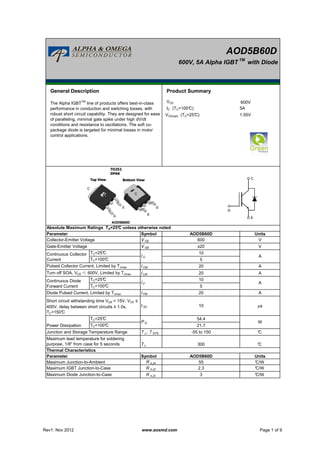
- 1. AOD5B60D 600V, 5A Alpha IGBT TM with Diode General Description Product Summary VCE IC (TC=100°C) 5A VCE(sat) (TC=25°C) 1.55V Symbol V CE The Alpha IGBTTM line of products offers best-in-class performance in conduction and switching losses, with robust short circuit capability. They are designed for ease of paralleling, minimal gate spike under high dV/dt conditions and resistance to oscillations. The soft co- package diode is targeted for minimal losses in motor control applications. V UnitsParameter Absolute Maximum Ratings TA=25°C unless otherwise noted AOD5B60D 600V Collector-Emitter Voltage 600 G C E AOD5B60D Top View TO252 DPAK Bottom View C G G E C E CE V GE I CM I LM Diode Pulsed Current, Limited by TJmax I FM t SC T J , T STG T L Symbol R θ JA R θ JC R θ JC °C/W3Maximum Diode Junction-to-Case °C/W2.3Maximum IGBT Junction-to-Case Maximum Junction-to-Ambient 10 µs TC=100°C Maximum lead temperature for soldering purpose, 1/8" from case for 5 seconds °C Power Dissipation P D Short circuit withstanding time VGE = 15V, VCE ≤ 400V, delay between short circuits ≥ 1.0s, TC=150°C Junction and Storage Temperature Range TC=25°C Thermal Characteristics 300 -55 to 150 54.4 20 °C/W55 21.7 °C 20 AOD5B60D Pulsed Collector Current, Limited by TJmax Gate-Emitter Voltage TC=100°C W Units A A Parameter ±20 V 20 A A Continuous Diode Forward Current TC=25°C I F 10 A TC=100°C Continuous Collector Current TC=25°C 5 10 5 I C Turn off SOA, VCE ≤ 600V, Limited by TJmax G C E AOD5B60D Top View TO252 DPAK Bottom View C G G E C E Rev1: Nov 2012 www.aosmd.com Page 1 of 9
- 2. AOD5B60D Symbol Min Typ Max Units BV CES Collector-Emitter Breakdown Voltage 600 - - V TJ=25°C - 1.55 1.8 TJ=125°C - 1.78 - TJ=150°C - 1.85 - TJ=25°C - 1.46 1.75 TJ=125°C - 1.36 - TJ=150°C - 1.3 - V GE(th) Gate-Emitter Threshold Voltage - 6 - V TJ=25°C - - 10 TJ=125°C - - 100 TJ=150°C - - 500 I GES Gate-Emitter Leakage Current - - ±100 nA g FS - 2.3 - S C ies - 367 - pF C oes - 34 - pF C res - 1.47 - pF Q g - 9.4 - nC Q ge - 3.15 - nC Q gc - 6.25 - nC I C(SC) - 21 - A R g - 3 - Ω t D(on) - 12 - ns t r - 15 - ns Collector-Emitter Saturation Voltage Output Capacitance Input Capacitance I CES Zero Gate Voltage Collector Current V F Diode Forward Voltage DYNAMIC PARAMETERS µA VCE=VGE, IC=1mA Electrical Characteristics (TJ=25°C unless otherwise noted) STATIC PARAMETERS Parameter Conditions Reverse Transfer Capacitance VGE=0V, VCE=25V, f=1MHz VCE=20V, IC=5A VCE=0V, VGE=±20V Forward Transconductance V CE(sat) IC=1mA, VGE=0V, TJ=25°C VGE=15V, IC=5A V VCE=600V, VGE=0V VGE=0V, IC=5A V Gate to Collector Charge Gate to Emitter Charge VGE=15V, VCE=480V, IC=5A SWITCHING PARAMETERS, (Load Inductive, TJ=25°C) Short circuit collector current, Max. 1000 short circuits, Delay between short circuits ≥ 1.0s VGE=15V, VCE=400V, RG=60Ω Total Gate Charge Gate Resistance VGE=0V, VCE=0V, f=1MHz Turn-On Rise Time Turn-On Delay Time TJ=25°Ct r - 15 - ns t D(off) - 82 - ns t f - 10 - ns E on - 0.14 - mJ E off - 0.04 - mJ E total - 0.18 - mJ t rr - 98 - ns Q rr - 0.23 - µC I rm - 4.4 - A t D(on) - 11 - ns t r - 16 - ns t D(off) - 110 - ns t f - 14 - ns E on - 0.18 - mJ E off - 0.08 - mJ E total - 0.26 - mJ t rr - 166 - ns Q rr - 0.4 - µC I rm - 5.2 - A THIS PRODUCT HAS BEEN DESIGNED AND QUALIFIED FOR THE CONSUMER MARKET. APPLICATIONS OR USES AS CRITICAL COMPONENTS IN LIFE SUPPORT DEVICES OR SYSTEMS ARE NOT AUTHORIZED. AOS DOES NOT ASSUME ANY LIABILITY ARISING OUT OF SUCH APPLICATIONS OR USES OF ITS PRODUCTS. AOS RESERVES THE RIGHT TO IMPROVE PRODUCT DESIGN, FUNCTIONS AND RELIABILITY WITHOUT NOTICE. Turn-Off Energy Turn-On Rise Time SWITCHING PARAMETERS, (Load Inductive, TJ=150°C) Diode Reverse Recovery Time Diode Reverse Recovery Charge Diode Peak Reverse Recovery Current TJ=25°C IF=5A,dI/dt=200A/µs,VCE=400V Turn-Off Delay Time TJ=25°C VGE=15V, VCE=400V, IC=5A, RG=60Ω, Parasitic Ιnductance=75nH Total Switching Energy Turn-Off Fall Time Turn-On Energy TJ=150°C IF=5A,dI/dt=200A/µs,VCE=400VDiode Reverse Recovery Charge Diode Peak Reverse Recovery Current Turn-On DelayTime TJ=150°C VGE=15V, VCE=400V, IC=5A, RG=60Ω, Parasitic Inductance=75nH Turn-On Rise Time Turn-Off Delay Time Turn-Off Fall Time Turn-On Energy Diode Reverse Recovery Time Turn-Off Energy Total Switching Energy Rev1: Nov 2012 www.aosmd.com Page 2 of 9
- 3. AOD5B60D □ TYPICAL ELECTRICAL AND THERMAL CHARACTERISTICS 0 5 10 15 20 25 30 35 40 0.0 0.5 1.0 1.5 2.0 2.5 3.0 IF(A) VF (V) Fig 4: Diode Characteristic 25°C 150°C -40°C 0 5 10 15 20 25 30 35 0 1 2 3 4 5 6 7 IC(A) VCE(V) Fig 1: Output Characteristic (Tj=25°C ) 9V 20V 17V 15V 11V VGE= 7V 13V 0 5 10 15 20 4 7 10 13 16 IC(A) VGE(V) Fig 3: Transfer Characteristic 150°C 25°C -40°CVCE=20V 0 5 10 15 20 25 30 0 1 2 3 4 5 6 7 IC(A) VCE(V) Fig 2: Output Characteristic (Tj=150°C ) VGE=7V 9V 20V 17V 15V 11V 13V 0 5 10 15 20 25 30 35 40 0.0 0.5 1.0 1.5 2.0 2.5 3.0 IF(A) VF (V) Fig 4: Diode Characteristic 25°C 150°C -40°C 0 5 10 15 20 25 30 35 0 1 2 3 4 5 6 7 IC(A) VCE(V) Fig 1: Output Characteristic (Tj=25°C ) 9V 20V 17V 15V 11V VGE= 7V 13V 0 5 10 15 20 4 7 10 13 16 IC(A) VGE(V) Fig 3: Transfer Characteristic 150°C 25°C -40°C 0 1 2 3 4 0 25 50 75 100 125 150 VCE(sat)(V) Temperature (°C) Fig 5: Collector-Emitter Saturation Voltage vs. Junction Temperature IC=10A IC=2.5A IC=5A 0 5 10 15 20 25 30 0 10 20 30 40 50 60 5 8 11 14 17 20 Current(A) Time(µµµµS) VGE (V) Fig 6: VGE vs. Short Circuit Time (VCE=400V,TC=25°C ) VCE=20V 0 5 10 15 20 25 30 0 1 2 3 4 5 6 7 IC(A) VCE(V) Fig 2: Output Characteristic (Tj=150°C ) VGE=7V 9V 20V 17V 15V 11V 13V Rev1: Nov 2012 www.aosmd.com Page 3 of 9
- 4. AOD5B60D □ TYPICAL ELECTRICAL AND THERMAL CHARACTERISTICS 1 10 100 10 100 1,000 Ic(A) VCE (V) Fig 10: Reverse Bias SOA (Tj=150°C,V GE=15V) 0 3 6 9 12 15 0 2 4 6 8 10 IC(A) Qg(nC) Fig 7: Gate-Charge Characteristics VCE=480V IC=5A 1 10 100 1000 0 5 10 15 20 25 30 35 40 Capacitance(pF) VCE(V) Fig 8: Capacitance Characteristic Cies Cres Coes 1 10 100 10 100 1,000 Ic(A) VCE (V) Fig 10: Reverse Bias SOA (Tj=150°C,V GE=15V) 0 3 6 9 12 15 0 2 4 6 8 10 IC(A) Qg(nC) Fig 7: Gate-Charge Characteristics VCE=480V IC=5A 0 10 20 30 40 50 60 25 50 75 100 125 150 PowerDisspation(W) TCASE(°C) Fig 11: Power Disspation as a Function of Case 1 10 100 1000 0 5 10 15 20 25 30 35 40 Capacitance(pF) VCE(V) Fig 8: Capacitance Characteristic Cies Cres Coes 0 2 4 6 8 10 25 50 75 100 125 150 CurrentratingIC(A) TCASE(°C) Fig 12: Current De-rating Rev1: Nov 2012 www.aosmd.com Page 4 of 9
- 5. AOD5B60D ≤ TYPICAL ELECTRICAL AND THERMAL CHARACTERISTICS 1 10 100 1000 0 3 6 9 12 SwitchingTime(nS) IC (A) Figure 13: Switching Time vs. IC (Tj=150°C,V GE=15V,VCE=400V,Rg=60ΩΩΩΩ) Td(off) Tf Td(on) Tr 1 10 100 1,000 10,000 0 100 200 300 400 500 600 SwitchingTime(nS) Rg (ΩΩΩΩ) Figure 14: Switching Time vs. Rg (Tj=150°C,V GE=15V,VCE=400V,IC=5A) Td(off) Tf Td(on) Tr 1 10 100 1000 0 50 100 150 200 SwitchingTime(nS) TJ (°C) Figure 15: Switching Time vs.Tj ( VGE=15V,VCE=400V,IC=5A,Rg=60ΩΩΩΩ) Td(off) Tf Td(on) Tr 0 2 4 6 8 10 0 30 60 90 120 150 VGE(TH)(V) TJ (°C) Figure 16: VGE(TH) vs. Tj 1 10 100 1000 0 3 6 9 12 SwitchingTime(nS) IC (A) Figure 13: Switching Time vs. IC (Tj=150°C,V GE=15V,VCE=400V,Rg=60ΩΩΩΩ) Td(off) Tf Td(on) Tr 1 10 100 1,000 10,000 0 100 200 300 400 500 600 SwitchingTime(nS) Rg (ΩΩΩΩ) Figure 14: Switching Time vs. Rg (Tj=150°C,V GE=15V,VCE=400V,IC=5A) Td(off) Tf Td(on) Tr 1 10 100 1000 0 50 100 150 200 SwitchingTime(nS) TJ (°C) Figure 15: Switching Time vs.Tj ( VGE=15V,VCE=400V,IC=5A,Rg=60ΩΩΩΩ) Td(off) Tf Td(on) Tr 0 2 4 6 8 10 0 30 60 90 120 150 VGE(TH)(V) TJ (°C) Figure 16: VGE(TH) vs. Tj Rev1: Nov 2012 www.aosmd.com Page 5 of 9
- 6. AOD5B60D ≤ TYPICAL ELECTRICAL AND THERMAL CHARACTERISTICS 0 0.1 0.2 0.3 0.4 0.5 0.6 0 3 6 9 12 E,SwitchIngEnergy(mJ) IC (A) Figure 17: Switching Loss vs. IC (Tj=150°C,V GE=15V,VCE=400V,Rg=60ΩΩΩΩ) Eoff Eon Etotal 0.0 0.1 0.2 0.3 0.4 0.5 0.6 0 100 200 300 400 500 600 SwitchingEnergy(mJ) Rg (ΩΩΩΩ) Figure 18: Switching Loss vs. Rg (Tj=150°C,V GE=15V,VCE=400V,IC=5A) Eoff Eon Etotal 0 0.1 0.2 0.3 0.4 0 25 50 75 100 125 150 175 SwitchingEnergy(mJ) TJ (°C) Eoff Eon Etotal 0.0 0.1 0.2 0.3 0.4 200 250 300 350 400 450 500 SwitchingEnergy(mJ) V (V) Eoff Eon Etotal 0 0.1 0.2 0.3 0.4 0.5 0.6 0 3 6 9 12 E,SwitchIngEnergy(mJ) IC (A) Figure 17: Switching Loss vs. IC (Tj=150°C,V GE=15V,VCE=400V,Rg=60ΩΩΩΩ) Eoff Eon Etotal 0.0 0.1 0.2 0.3 0.4 0.5 0.6 0 100 200 300 400 500 600 SwitchingEnergy(mJ) Rg (ΩΩΩΩ) Figure 18: Switching Loss vs. Rg (Tj=150°C,V GE=15V,VCE=400V,IC=5A) Eoff Eon Etotal 0 0.1 0.2 0.3 0.4 0 25 50 75 100 125 150 175 SwitchingEnergy(mJ) TJ (°C) Figure 19: Switching Loss vs. Tj (VGE=15V,VCE=400V,IC=5A,Rg=60ΩΩΩΩ) Eoff Eon Etotal 0.0 0.1 0.2 0.3 0.4 200 250 300 350 400 450 500 SwitchingEnergy(mJ) VCE (V) Figure 20: Switching Loss vs. VCE (Tj=150°C,V GE=15V,IC=5A,Rg=60ΩΩΩΩ) Eoff Eon Etotal Rev1: Nov 2012 www.aosmd.com Page 6 of 9
- 7. AOD5B60D □ TYPICAL ELECTRICAL AND THERMAL CHARACTERISTICS 0 3 6 9 12 15 18 0 50 100 150 200 250 300 0 3 6 9 12 S Trr(nS) IS (A) Fig 24: Diode Reverse Recovery Time and Softness Factor vs. Conduction Current (VGE=15V,VCE=400V, di/dt=200A/µµµµs) 150°C 25°C 150°C 25°C Trr S 0 5 10 15 20 25 30 35 40 0 100 200 300 400 500 600 700 800 0 3 6 9 12 Irm(A) Qrr(nC) IF(A) Fig 23: Diode Reverse Recovery Charge and Peak Current vs. Conduction Current (VGE=15V,VCE=400V, di/dt=200A/µµµµs) 25°C 150°C 150°C 25°C Qrr Irm 13V 1.E-08 1.E-07 1.E-06 1.E-05 1.E-04 1.E-03 0 25 50 75 100 125 150 175 ICE(S)(A) Temperature (°C ) Fig 21: Reverse Leakage Current vs. Junction Temperature VCE=600V VCE=400V 0.2 0.7 1.2 1.7 2.2 0 25 50 75 100 125 150 175 VSD(V) Temperature (°C ) Fig 22: Diode Forward Voltage vs. Junction Temperature 15A 10A 5A IF=1A 0 3 6 9 12 15 18 0 50 100 150 200 250 300 0 3 6 9 12 S Trr(nS) IS (A) Fig 24: Diode Reverse Recovery Time and Softness Factor vs. Conduction Current (VGE=15V,VCE=400V, di/dt=200A/µµµµs) 150°C 25°C 150°C 25°C Trr S 0 5 10 15 20 25 30 35 40 0 100 200 300 400 500 600 700 800 0 3 6 9 12 Irm(A) Qrr(nC) IF(A) Fig 23: Diode Reverse Recovery Charge and Peak Current vs. Conduction Current (VGE=15V,VCE=400V, di/dt=200A/µµµµs) 25°C 150°C 150°C 25°C Qrr Irm 13V 1.E-08 1.E-07 1.E-06 1.E-05 1.E-04 1.E-03 0 25 50 75 100 125 150 175 ICE(S)(A) Temperature (°C ) Fig 21: Reverse Leakage Current vs. Junction Temperature VCE=600V VCE=400V 0.2 0.7 1.2 1.7 2.2 0 25 50 75 100 125 150 175 VSD(V) Temperature (°C ) Fig 22: Diode Forward Voltage vs. Junction Temperature 15A 10A 5A IF=1A 0 4 8 12 16 20 0 40 80 120 160 200 100 200 300 400 500 600 700 800 900 S Trr(nS) di/dt (A/µµµµS) Fig 26: Diode Reverse Recovery Time and Softness Factor vs. di/dt (VGE=15V,VCE=400V,IF=5A) 25°C 150°C 25°C 150°C Trr S 0 10 20 30 40 50 60 0 100 200 300 400 500 600 100 200 300 400 500 600 700 800 900 Irm(A) Qrr(nC) di/dt (A/µµµµS) Fig 25: Diode Reverse Recovery Charge and Peak Current vs. di/dt (VGE=15V,VCE=400V,IF=5A) 150°C 25°C 150°C 25°C Qrr Irm Rev1: Nov 2012 www.aosmd.com Page 7 of 9
- 8. AOD5B60D □ TYPICAL ELECTRICAL AND THERMAL CHARACTERISTICS 0.001 0.01 0.1 1 10 1E-06 1E-05 0.0001 0.001 0.01 0.1 1 10 ZθθθθJCNormalizedTransient ThermalResistance Pulse Width (s) Figure 27: Normalized Maximum Transient Thermal Impedance for IGBT D=Ton/T TJ,PK=TC+PDM.ZθJC.RθJC RθJC=2.3°C/W In descending order D=0.5, 0.3, 0.1, 0.05, 0.02, 0.01, single pulse Single Pulse Ton T PD 0.001 0.01 0.1 1 10 1E-05 0.0001 0.001 0.01 0.1 1 10 ZθθθθJCNormalizedTransient ThermalResistance Pulse Width (s) Figure 28: Normalized Maximum Transient Thermal Impedance for Diode D=Ton/T TJ,PK=TC+PDM.ZθJC.RθJC RθJC=3°C/W In descending order D=0.5, 0.3, 0.1, 0.05, 0.02, 0.01, single pulse Single Pulse Ton T PD 0.001 0.01 0.1 1 10 1E-06 1E-05 0.0001 0.001 0.01 0.1 1 10 ZθθθθJCNormalizedTransient ThermalResistance Pulse Width (s) Figure 27: Normalized Maximum Transient Thermal Impedance for IGBT D=Ton/T TJ,PK=TC+PDM.ZθJC.RθJC RθJC=2.3°C/W In descending order D=0.5, 0.3, 0.1, 0.05, 0.02, 0.01, single pulse Single Pulse Ton T PD 0.001 0.01 0.1 1 10 1E-05 0.0001 0.001 0.01 0.1 1 10 ZθθθθJCNormalizedTransient ThermalResistance Pulse Width (s) Figure 28: Normalized Maximum Transient Thermal Impedance for Diode D=Ton/T TJ,PK=TC+PDM.ZθJC.RθJC RθJC=3°C/W In descending order D=0.5, 0.3, 0.1, 0.05, 0.02, 0.01, single pulse Single Pulse Ton T PD Rev1: Nov 2012 www.aosmd.com Page 8 of 9
- 9. AOD5B60D Rev1: Nov 2012 www.aosmd.com Page 9 of 9