
Recommended
More Related Content
What's hot
What's hot (19)
Similar to Operating system
Similar to Operating system (20)
Recently uploaded
Recently uploaded (20)
Operating system
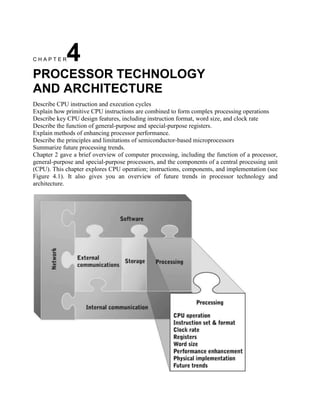
- 1. CHAPTER 4 PROCESSOR TECHNOLOGY AND ARCHITECTURE Describe CPU instruction and execution cycles Explain how primitive CPU instructions are combined to form complex processing operations Describe key CPU design features, including instruction format, word size, and clock rate Describe the function of general-purpose and special-purpose registers. Explain methods of enhancing processor performance. Describe the principles and limitations of semiconductor-based microprocessors Summarize future processing trends. Chapter 2 gave a brief overview of computer processing, including the function of a processor, general-purpose and special-purpose processors, and the components of a central processing unit (CPU). This chapter explores CPU operation; instructions, components, and implementation (see Figure 4.1). It also gives you an overview of future trends in processor technology and architecture.
- 2. CPU OPERATION: Recall from Chapter 2 that a CPU has three primary components: the control unit, the arithmetic logic unit (ALU), and a set of registers (see Figure 4.2). The control unit moves data and instructions between main memory and registers, and the ALU performs all computation and comparison operations. Registers are storage locations that hold inputs and outputs for the ALU. A complex chain of events occurs when the CPU executes a program. To start, the control unit reads the first instruction from primary storage. It then stores the instruction in a register and, if necessary, reads data inputs from primary storage and stores them in registers. If the instruction is a computation or comparison instruction, the control unit signals the ALU what function to perform, where the input data is located, and where to store the output data. The control unit handles executing instructions to move data to memory, I/O devices, or secondary storage. When the first instruction has been executed, the next instruction is read and executed. This process continues until the program s final instruction has been executed. FIGURE 4.1 106 The actions the CPU performs can be divided into two groups the fetch cycle (or instruction cycle) and the execution cycle. During the fetch cycle, data inputs are prepared for
- 3. transformation into data outputs. During the execution cycle, the transformation takes place and data output is stored. The CPU alternates constantly between fetch and execution cycles. Figure 4.3 shows the flow between fetch and execution cycles (denoted by solid arrows) and data and instruction movement (denoted by dashed arrows). During the fetch cycle, the control unit does the following: Fetches an instruction from primary storage Increments a pointer to the location of the next instruction Separates the instruction into components the instruction code (or number) and the data inputs to the instruction Stores each component in a separate register During the execution cycle, the ALU does the following: Retrieves the instruction code from a register Retrieves data inputs from registers Passes data inputs through internal circuits to perform the addition, subtraction, or other data transformation Stores the result in a register http://www.scribd.com/doc/78728814/Operating-System
- 4. FIGURE 4.2 CPU components: At the conclusion of the execution cycle, a new fetch cycle is started. The control unit keeps track of the next program instruction location by incrementing a pointer after each fetch. The second program instruction is retrieved during the second fetch cycle, the third instruction is retrieved during the third fetch cycle, and so forth.
- 5. CPU REGISTERS: Registers play two primary roles in CPU operation. First, they provide a temporary storage area for data the currently executing program needs quickly or frequently. Second, they store information about the currently executing program and CPU status for example, the address of the next program instruction, error messages, and signals from external devices. General-Purpose Registers: General-purpose registers are used only by the currently executing program. They typically hold intermediate results or frequently used data values, such as loop counters or array indexes. Register accesses are fast because registers are implemented in the CPU. In contrast, storing and retrieving from primary storage is much slower. Using registers to store data needed immediately or frequently increases program execution speed by avoiding wait states. Adding general-purpose registers increases execution speed but only up to a point. Any process or program has a limited number of intermediate results or frequently used data items, so CPU designers try to find the optimal balance among the number of general purpose registers, the extent to which a typical process will use these registers, and the cost of implementing these registers. As the cost of producing registers has decreased, their number has increased. Current CPUs typically provide several dozen general-purpose registers. Special-Purpose Registers Every processor has special-purpose registers used by the CPU for specific purposes. Some of the more important special-purpose registers are as follows: Instruction register Instruction pointer Program status word When the control unit fetches an instruction from memory, it stores it in the instruction register. The control unit then extracts the op code and operands from the instruction and performs any additional data movement operations needed to prepare for execution. The process of extracting the op code and operands, loading data inputs, and signaling the ALU is called instruction decoding. The instruction pointer (IP) can also be called the program counter. Recall that the CPU alternates between the instruction (fetch and decode) and execution (data movement or transformation) cycles. At the end of each execution cycle, the control unit starts the next fetch cycle by retrieving the next instruction from memory. This instruction saddress is stored in the instruction pointer, and the control unit increments the instruction pointer during or immediately after each fetch cycle. The CPU deviates from sequential execution only if a BRANCH instruction is executed. A BRANCH is implemented by overwriting the instruction pointer s value with the address of the instruction to which the BRANCH is directed. An unconditional BRANCH instruction is actually a MOVE from the branch operand, which contains the branch address, to the instruction pointer.
- 6. The program status word (PSW) contains data describing the CPU status and the currently executing program. Each bit in the PSW is a separate Boolean variable, sometimes called a flag, representing one data item. The content and meaning of flags vary widely from one CPU to another. In general, PSW flags have three main uses: Store the result of a comparison operation. Control conditional BRANCH execution. Indicate actual or potential error conditions. The sample program shown previously in Figure 4.8 performed comparison by using the XOR, ADD, and SHIFT instructions. The result was stored in a general-purpose register and interpreted as a Boolean value. This method was used because the instruction set was limited. Most CPUs provide one or more COMPARE instructions. COMPARE takes two operands and determines whether the first is less than, equal to, or greater than the second. Because there are three possible conditions, the result can’t be stored in a single Boolean variable. Most CPUs use two PSW flags to store a COMPARE s result. One flag is set to true if the operands are equal, and the other flag indicates whether the first operand is greater than or less than the second. If the first flag is true, the second flag is ignored. To implement program branches based on a COMPARE result, two additional conditional BRANCH instructions are provided: one based on the equality flag and the other based on the less-than or greater-than flag. Using COMPARE with related conditional BRANCH instructions simplifies machine-language programs, which speeds up their execution. Other PSW flags represent status conditions resulting from the ALU executing instructions. Conditions such as overflow, underflow, or an attempt to perform an undefined operation (dividing by zero, for example) are represented by PSW flags. After each execution cycle, the control unit tests PSW flags to determine whether an error has occurred. They can also be tested by an OS or an application program to determine appropriate error messages and corrective actions.
- 7. BIOS updates CD or DVD drive drivers and firmware Controllers Display drivers Keyboard drivers Mouse drivers Modem drivers Motherboard drivers and updates Network card drivers Printer drivers Removable media drivers Scanner drivers Sound card drivers Video drivers Audio & Sound Drivers Bluetooth Drivers Digital Camera Drivers Fax Driver
- 8. Graphics and Video Card Keyboard / Mouse Drivers Modem Driver Monitor Drivers MP3 Player Driver Printer Drivers Scanner Drivers Webcam Drivers Wireless & Network Drivers USB Drivers A typical computer system has a variety of primary and secondary storage devices. The CPU and a small amount of high-speed RAM usually occupy the same chip. Slower RAM on separate chips composes the bulk of primary storage. One or more magnetic disk drives are usually complemented by an optical disc drive and at least one form of removable magnetic storage. The range of storage devices in a single computer system forms a memory-storage hierarchy, as shown in Figure 5.3. Cost and access speed generally decrease as you move down the hierarchy. Because of lower cost, capacity tends to increase as you move down the hierarchy. A computer designer or purchaser attempts to find an optimal mix of cost and performance for a particular purpose.
- 9. As discussed, the critical performance characteristics of primary storage devices are access speed and data transfer unit size. Primary storage devices must closely match CPU speed and word size to avoid wait states. CPU and primary storage technologies have evolved in tandem in other wor ds, CPU technology improvements are applied to the construction of primary storage devices. Storing Electrical Signals: Data is represented in the CPU as digital electrical signals, which are also the basis of data transmission for all devices attached to the system bus. Any storage device or controller must accept electrical signals as input and generate electrical signals as output. Electrical power can be stored directly by various devices, including batteries and capacitors. Unfortunately, there s a tradeoff between access speed and volatility. Batteries are quite slow to accept and regenerate electrical current. With repeated use, they also lose their capability to accept a charge. Capacitors can charge and discharge much faster than batteries. However, small capacitors lose their charge fairly rapidly and require a fresh injection of electrical current at regular intervals (hundreds or thousands of times per second). An electrical signal can be stored indirectly by using its energy to alter the state of a device, such as a mechanical switch, or a substance, such as a metal. An inverse process regenerates an equivalent electrical signal. For example, electrical current can generate a magnetic field. The magnetic field s strength can induce a permanent magnetic charge in a nearby metallic compound, thus writing the bit value to the metallic compound. To read the stored value, the
- 10. stored magnetic charge is used to generate an electrical signal equivalent to the one used to create the original magnetic charge. Magnetic polarity, which is positive or negative, can represent the values 0 and 1. Early computers implemented primary storage as rings of ferrous material (iron and iron compounds), a technology called core memory. These rings, or cores, are embedded in a two- dimensional wire mesh. Electricity sent through two wires induces a magnetic charge in one metallic ring. The charge s polarity depends on the direction of electrical flow through the wires. Modern computers use memory implemented with semiconductors. Basic types of semi conduc tor memory include random access memory and nonvolatile memory. There are many variations of each memory type, described in the following sections. Random Access Memory: Random access memory (RAM) is a generic term describing primary storage devices with the following characteristics: Microchip implementation with semiconductors Capability to read and write with equal speed Random access to stored bytes, words, or larger data units RAM is fabricated in the same manner as microprocessors. You might assume that microprocessor clock rates are well matched to RAM access speeds. Unfortunately, this isn’t the case for many reasons, including the following: Reading and writing many bits in parallel requires additional circuitry. When RAM and micro processors are on separate chips, there are delays when moving data from one chip to another. There are two basic RAM types and several variations of each type. Static RAM (SRAM) is implemented entirely with transistors. The basic storage unit is a flip-flop circuit. (See Figure 5.4). Each flip-flop circuit uses two transistors to store 1 bit. Additional transistors (typically two or four) perform read and write operations. A flip-flop circuit is an electrical switch that remembers its last position; one position represents 0 and the other represents 1. These circuits require a continuous supply of electrical power to maintain their positions. Therefore, SRAM is volatile unless a continuous supply of power can be guaranteed. mildly destructive, resulting in storage cell destruction after 100,000 or more write operations. Because of its slower write speed and limited number of write cycles, flash RAM currently has limited applications. It s used to store firmware programs, such as the system BIOS, that aren t changed frequently and are loaded into memory when a computer powers up. Flash RAM is also used in portable secondary storage devices, such as compact flash cards in digital cameras and USB flash drives. These storage devices typically mimic the behavior of a portable magnetic disk drive when connected to a computer system. Flash RAM is also beginning to challenge magnetic disk drives as the dominant secondary storage technology (see Technology Focus: Solid-State Drives later in this chapter). Other NVM
- 11. technologies under development could overcome some shortcomings of flash RAM. Two promising candidates are magnetoresistive RAM and phase-change memory. Magnetoresistive RAM (MRAM) stores bit values by using two magnetic elements, one with fixed polarity and the other with polarity that changes when a bit is written. The second magnetic element s polarity determines whether a current passing between the elements encounters low (a 0 bit) or high (a 1 bit) resistance. The latest MRAM generations have read and write speeds comparable with SRAM and densities comparable with DRAM, which make MRAM a potential replacement for both these RAM types. In addition, MRAM doesn’t t degrade with repeated writes, which gives it better longevity than conventional flash RAM. Phase-change memory (PCM), also known as phase-change RAM (PRAM or PCRAM), uses a glasslike compound of germanium, antimony, and tellurium (GST). When heated to the correct temperatures, GST can switch between amorphous and crystalline states. The amorphous state exhibits low reflectivity (useful in rewritable optical storage media) and high electrical resistance. The crystalline state exhibits high reflectivity and low electrical resistance. PCM has lower storage density and slower read times than conventional flash RAM, but its write time is much faster, and it doesn t wear out as quickly. Memory Packaging Memory packaging is similar to microprocessor packaging. Memory circuits are embedded in microchips, and groups of chips are packed on a small circuit board that can be installed or removed easily from a computer system. Early RAM and ROM circuits were packaged in dual inline packages (DIPs). Installing a DIP on a printed circuit board is a tedious and precise operation. Also, single DIPs mounted on the board surface occupy a large portion of the total surface area. In the late 1980s, memory manufacturers adopted the single inline memory module (SIMM) as a standard RAM package. Each SIMM incorporates multiple DIPs on a tiny printed circuit board. The edge of the circuit board has a row of electrical contacts, and the entire package is designed to lock into a SIMM slot on a motherboard. The double inline memory module (DIMM), a newer packaging standard, is essentially a SIMM with independent electrical contacts on both sides of the module, as shown in Figure 5.5.
- 12. Current microprocessors include a small amount of on-chip memory (described in Chapter 6). As fabrication techniques improve, the amount of memory that can be packaged with the CPU on a single chip will grow. The logical extension of this trend is placing a CPU and all its primary storage on a single chip, which would minimize or eliminate the current gap between microprocessor clock rates and memory access speeds. NOTE Although main memory isn t currently implemented as part of the CPU, the CPU s need to load instructions and data from memory and store processing results requires close coordination between both devices. Specifically, the physical organization of memory, the organization of programs and data in memory, and the methods of referencing specific memory locations are critical design issues for both primary storage devices and processors. These topics are discussed in Chapter 11.