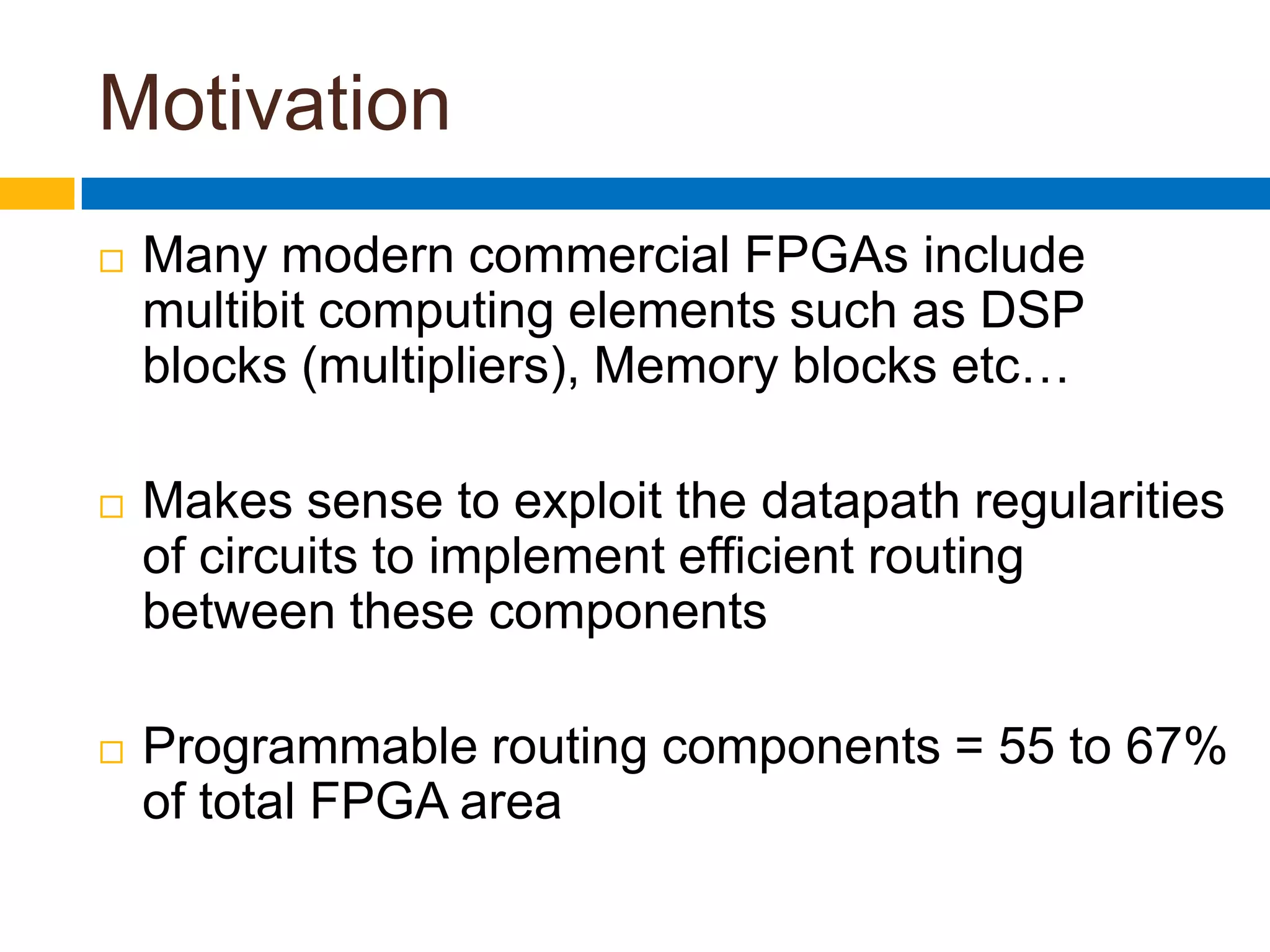
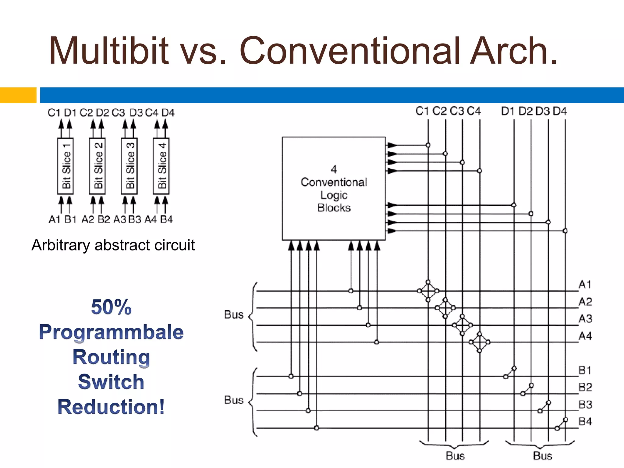
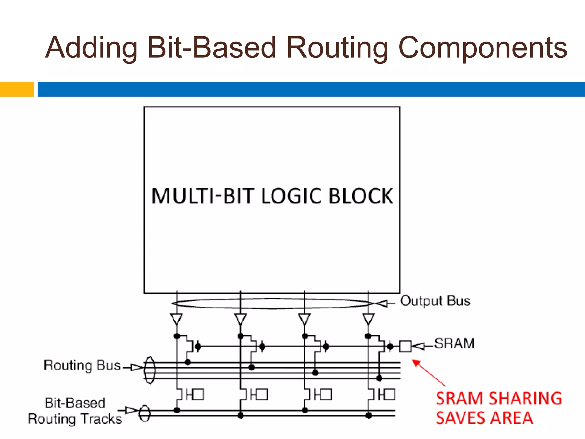
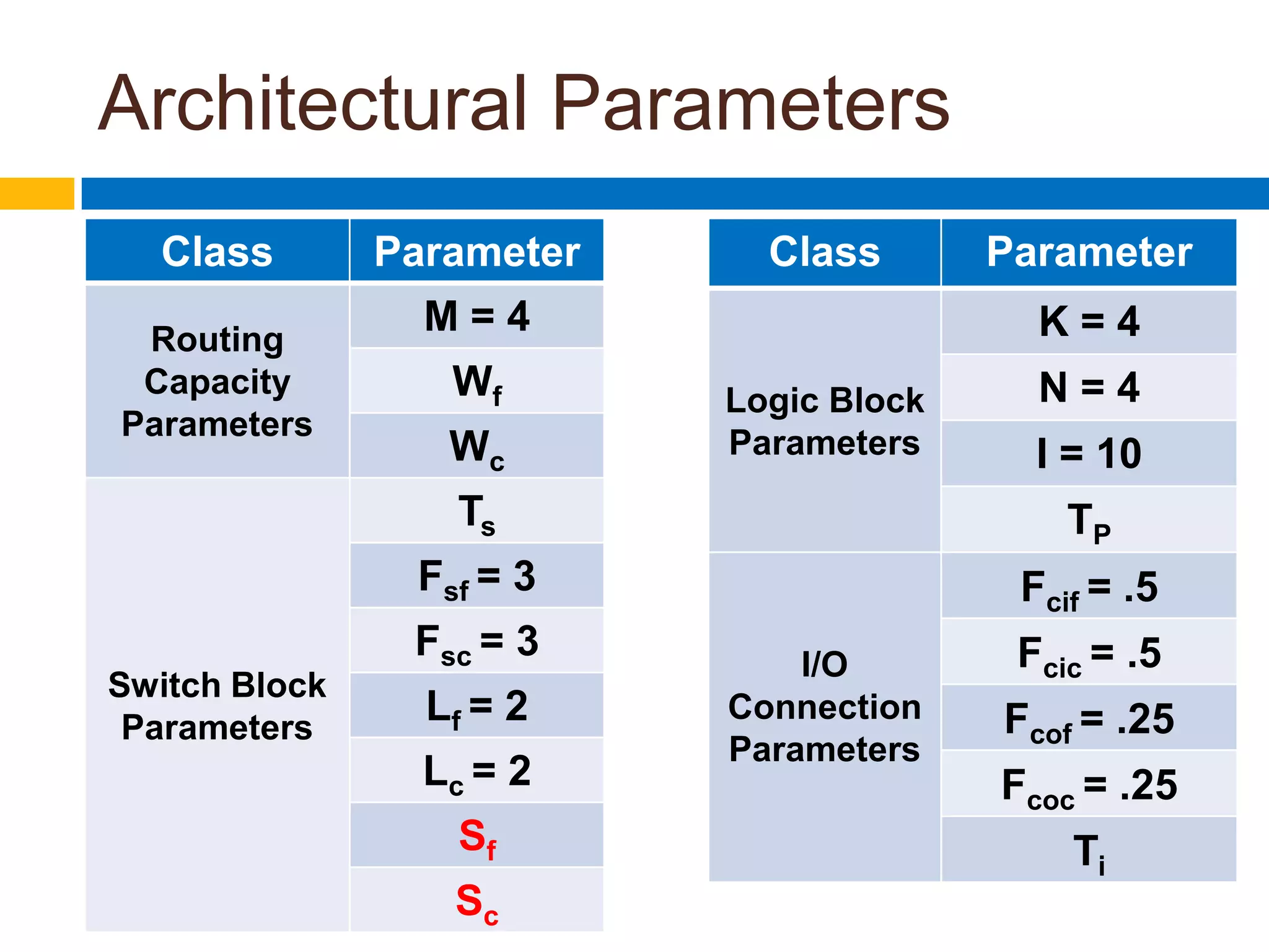
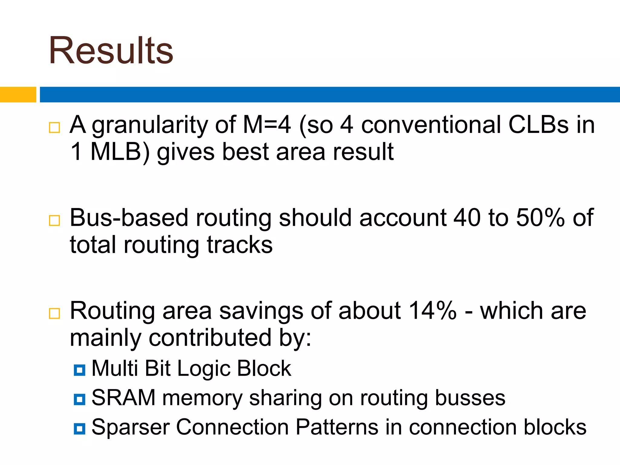
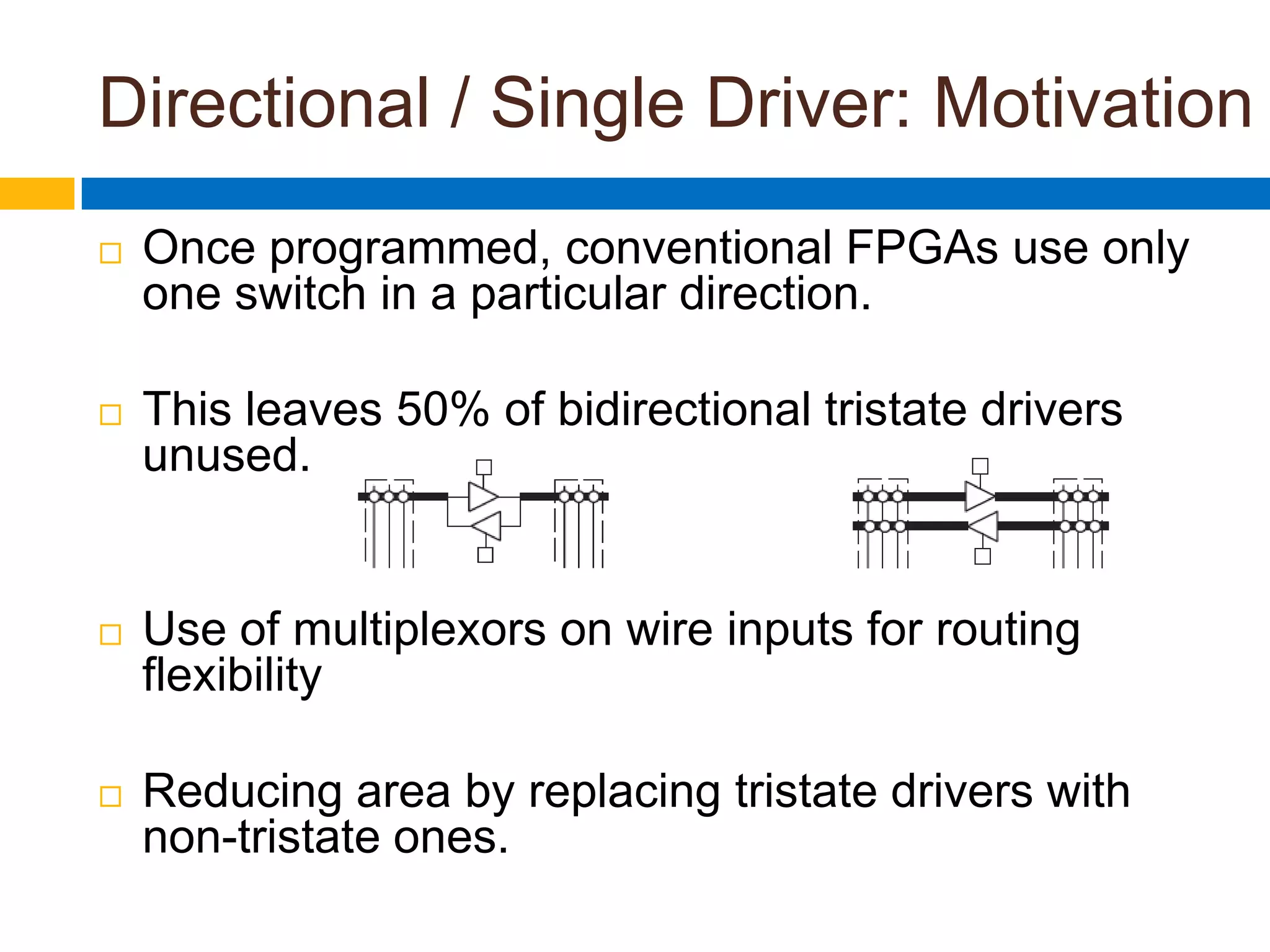
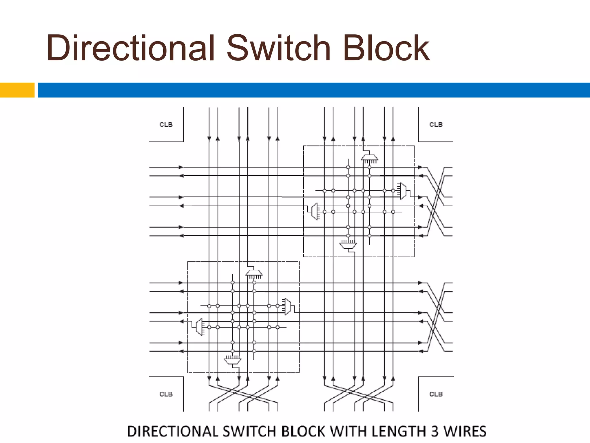
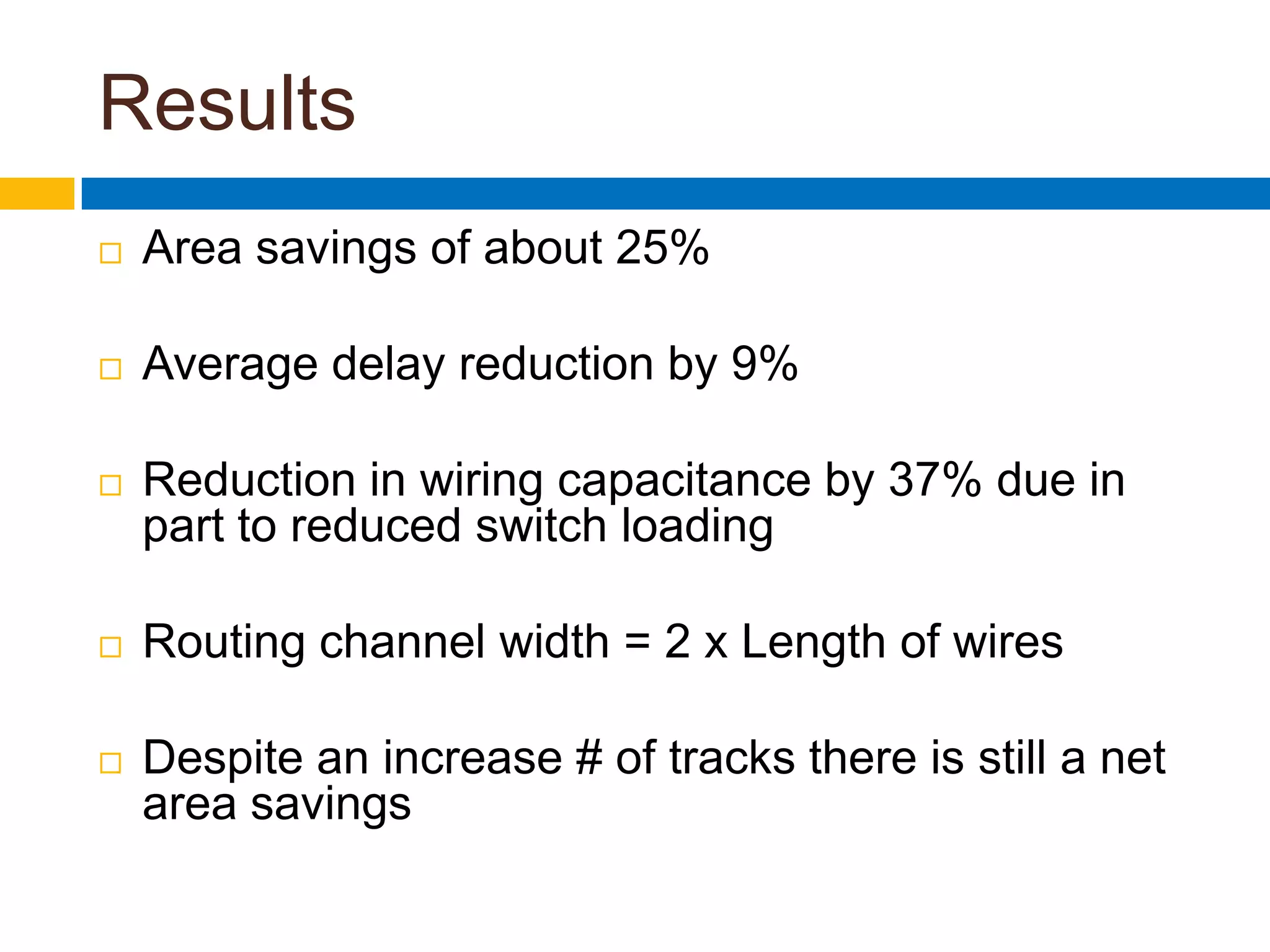
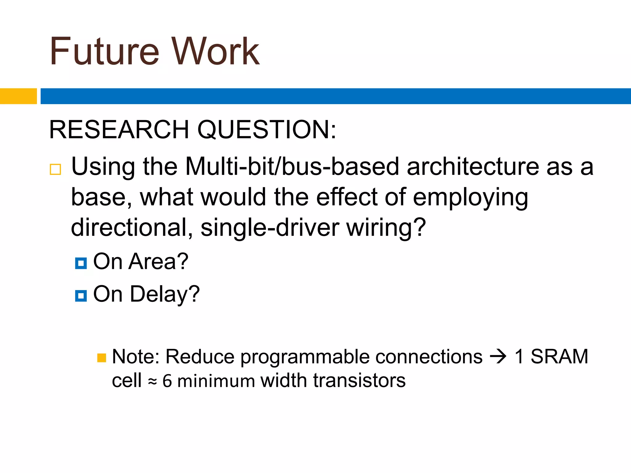
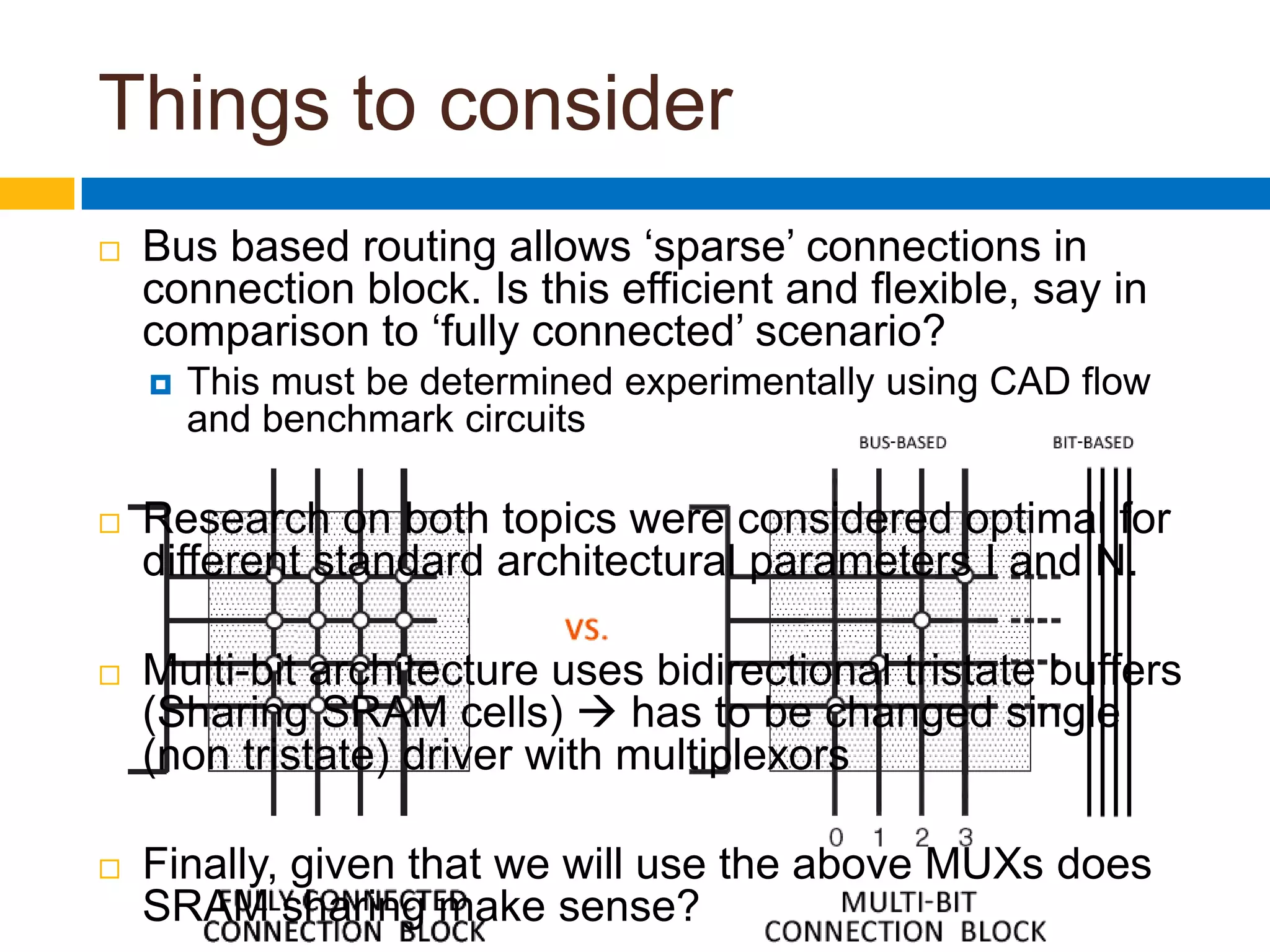
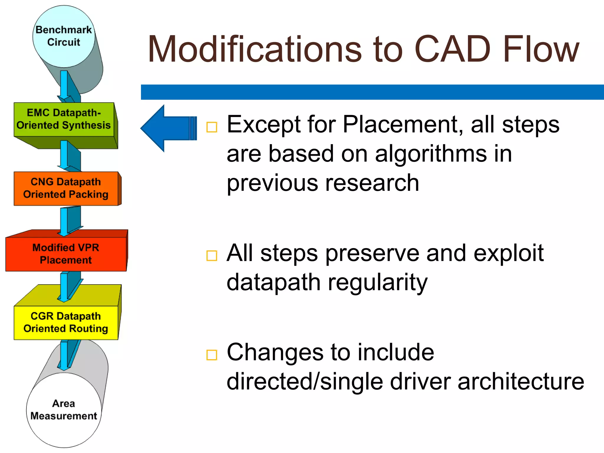
Area Efficient FPGA Architecture for Datapath CircuitsOmesh Mutukuda (MASc. candidate)Supervised by Dr. Andy Ye  &  co-supervised by Dr. Gul Khan
FPGA  Architectural Overview
“Island Style”FPGA Basics“FULLY CONNECTED”
Multibit / Bus-based Architecture
MotivationMany modern commercial FPGAs include multibit computing elements such as DSP blocks (multipliers), Memory blocks etc…Makes sense to exploit the datapath regularities of circuits to implement efficient routing between these componentsProgrammable routing components = 55 to 67% of total FPGA area
Multibit vs. Conventional Arch.Arbitrary abstract circuit50% Programmbale RoutingSwitch Reduction!
Adding Bit-Based Routing ComponentsPure bus based connections force the router in a CAD tool to use busses for irregular bit based signalsThis causes loss of area efficiencyWhat about a combination of bus-based and bit-based routing?
Architectural Parameters
ResultsA granularity of M=4 (so 4 conventional CLBs in 1 MLB) gives best area resultBus-based routing should account 40 to 50% of total routing tracksRouting area savings of about 14% - which are mainly contributed by:Multi Bit Logic BlockSRAM memory sharing on routing bussesSparser Connection Patterns in connection blocks
Directional / Single-Driver Wires
Directional / Single Driver: MotivationOnce programmed, conventional FPGAs use only one switch in a particular direction.This leaves 50% of bidirectional tristate drivers unused.Use of multiplexors on wire inputs for routing flexibility Reducing area by replacing tristate drivers with non-tristate ones.
Directional Switch BlockBIDIRECTIONAL              DIRECTIONAL
ResultsArea savings of about 25%Average delay reduction by 9%Reduction in wiring capacitance by 37% due in part to reduced switch loadingRouting channel width = 2 x Length of wiresDespite an increase # of tracks there is still a net area savings
Future Work
Future WorkRESEARCH QUESTION:Using the Multi-bit/bus-based architecture as a base, what would the effect of employing directional, single-driver wiring?On Area?On Delay?Note: Reduce programmable connections  1 SRAM cell ≈ 6 minimum width transistors
Things to considerBus based routing allows ‘sparse’ connections in connection block. Is this efficient and flexible, say in comparison to ‘fully connected’ scenario?This must be determined experimentally using CAD flow and benchmark circuitsResearch on both topics were considered optimal for different standard architectural parameters I and N.Multi-bit architecture uses bidirectional tristate buffers (Sharing SRAM cells)  has to be changed single (non tristate) driver with multiplexorsFinally, given that we will use the above MUXs does SRAM sharing make sense?
Modifications to CAD FlowExcept for Placement, all steps are based on algorithms in previous researchAll steps preserve and exploit datapath regularityChanges to include directed/single driver architecture
References[1]	Ye, A.; Rose, J., "Using bus-based connections to improve field-programmable gate-array 	density for implementing datapath circuits," Very Large Scale Integration (VLSI) Systems, 	IEEE Transactions on , vol.14, no.5, pp. 462-473, May 2006[2]	Lemieux, G.; Lee, E.; Tom, M.; Yu, A., "Directional and single-driver wires in FPGA 	interconnect," Field-Programmable Technology, 2004. Proceedings. 2004 IEEE 	International Conference on , vol., no., pp. 41-48, 6-8 Dec. 2004[3]	A. Ye, J. Rose, and D. Lewis, “Synthesizing datapath circuits for FPGAs with emphasis on 	area minimization,” in Proc. Int. Conf. Field-Programmable Technol., 2002, pp. 219–227.[4]	 A.Ye and J. Rose, “Using multi-bit logic blocks and automated packing to improve field-	programmable gate array density for implementing datapath circuits,” in Proc. Int. Conf. 	Field-Programmable Technol., 2004, pp. 129–136.[5]	A. Marquardt, V. Betz and J. Rose, “Using Cluster-Based Logic Blocks and Timing-Driven 	Packing to Improve FPGA Speed and Density”, ACM/SIGDA FPGA 99, 1999, pp. 37-46.[6]	A. Ye, “Field-Programmable Gate Array Architectures and Algorithms Optimized for 	Implementing Datapath Circuits,” Ph.D. thesis, Univ. Toronto, Dept. Elect. Comput. Eng., 	Univ. Toronto, ON, Canada, 2004 [Online]. Available: 	(http://www.eecg.toronto.edu/~jayar/pubs/theses/Ye/ AndyYe.pdf)
Questions?...The End

FPGA Architecture Presentation

  • 1.
    Area Efficient FPGAArchitecture for Datapath CircuitsOmesh Mutukuda (MASc. candidate)Supervised by Dr. Andy Ye & co-supervised by Dr. Gul Khan
  • 2.
  • 3.
  • 4.
  • 5.
    MotivationMany modern commercialFPGAs include multibit computing elements such as DSP blocks (multipliers), Memory blocks etc…Makes sense to exploit the datapath regularities of circuits to implement efficient routing between these componentsProgrammable routing components = 55 to 67% of total FPGA area
  • 6.
    Multibit vs. ConventionalArch.Arbitrary abstract circuit50% Programmbale RoutingSwitch Reduction!
  • 7.
    Adding Bit-Based RoutingComponentsPure bus based connections force the router in a CAD tool to use busses for irregular bit based signalsThis causes loss of area efficiencyWhat about a combination of bus-based and bit-based routing?
  • 8.
  • 9.
    ResultsA granularity ofM=4 (so 4 conventional CLBs in 1 MLB) gives best area resultBus-based routing should account 40 to 50% of total routing tracksRouting area savings of about 14% - which are mainly contributed by:Multi Bit Logic BlockSRAM memory sharing on routing bussesSparser Connection Patterns in connection blocks
  • 10.
  • 11.
    Directional / SingleDriver: MotivationOnce programmed, conventional FPGAs use only one switch in a particular direction.This leaves 50% of bidirectional tristate drivers unused.Use of multiplexors on wire inputs for routing flexibility Reducing area by replacing tristate drivers with non-tristate ones.
  • 12.
  • 13.
    ResultsArea savings ofabout 25%Average delay reduction by 9%Reduction in wiring capacitance by 37% due in part to reduced switch loadingRouting channel width = 2 x Length of wiresDespite an increase # of tracks there is still a net area savings
  • 14.
  • 15.
    Future WorkRESEARCH QUESTION:Usingthe Multi-bit/bus-based architecture as a base, what would the effect of employing directional, single-driver wiring?On Area?On Delay?Note: Reduce programmable connections  1 SRAM cell ≈ 6 minimum width transistors
  • 16.
    Things to considerBusbased routing allows ‘sparse’ connections in connection block. Is this efficient and flexible, say in comparison to ‘fully connected’ scenario?This must be determined experimentally using CAD flow and benchmark circuitsResearch on both topics were considered optimal for different standard architectural parameters I and N.Multi-bit architecture uses bidirectional tristate buffers (Sharing SRAM cells)  has to be changed single (non tristate) driver with multiplexorsFinally, given that we will use the above MUXs does SRAM sharing make sense?
  • 17.
    Modifications to CADFlowExcept for Placement, all steps are based on algorithms in previous researchAll steps preserve and exploit datapath regularityChanges to include directed/single driver architecture
  • 18.
    References[1] Ye, A.; Rose,J., "Using bus-based connections to improve field-programmable gate-array density for implementing datapath circuits," Very Large Scale Integration (VLSI) Systems, IEEE Transactions on , vol.14, no.5, pp. 462-473, May 2006[2] Lemieux, G.; Lee, E.; Tom, M.; Yu, A., "Directional and single-driver wires in FPGA interconnect," Field-Programmable Technology, 2004. Proceedings. 2004 IEEE International Conference on , vol., no., pp. 41-48, 6-8 Dec. 2004[3] A. Ye, J. Rose, and D. Lewis, “Synthesizing datapath circuits for FPGAs with emphasis on area minimization,” in Proc. Int. Conf. Field-Programmable Technol., 2002, pp. 219–227.[4] A.Ye and J. Rose, “Using multi-bit logic blocks and automated packing to improve field- programmable gate array density for implementing datapath circuits,” in Proc. Int. Conf. Field-Programmable Technol., 2004, pp. 129–136.[5] A. Marquardt, V. Betz and J. Rose, “Using Cluster-Based Logic Blocks and Timing-Driven Packing to Improve FPGA Speed and Density”, ACM/SIGDA FPGA 99, 1999, pp. 37-46.[6] A. Ye, “Field-Programmable Gate Array Architectures and Algorithms Optimized for Implementing Datapath Circuits,” Ph.D. thesis, Univ. Toronto, Dept. Elect. Comput. Eng., Univ. Toronto, ON, Canada, 2004 [Online]. Available: (http://www.eecg.toronto.edu/~jayar/pubs/theses/Ye/ AndyYe.pdf)
  • 19.