A Critique of the Proposed National Education Policy Reform
Larrabee
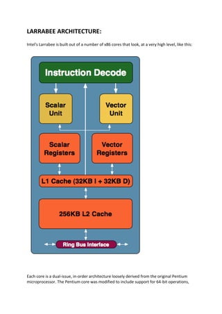
1. LARRABEE ARCHITECTURE:
Intel's Larrabee is built out of a number of x86 cores that look, at a very high level, like this:
Each core is a dual-issue, in-order architecture loosely derived from the original Pentium
microprocessor. The Pentium core was modified to include support for 64-bit operations,
2. the updates to the x86 instruction set, larger caches, 4-way SMT/Hyper Threading and a 16-
wide vector ALU.
While the team that ended up working on Atom may have originally worked on the Larrabee
cores, there are some significant differences between Larrabee and Atom. Atom is geared
towards much higher single threaded performance, with a deeper pipeline, a larger L2 cache
and additional microarchitectural tweaks to improve general desktop performance.
Intel Larrabee
Core
Intel Pentium
Core (P54C)
Intel Atom Core
Manufacturing
Process
45nm 0.60µm 45nm
Simultaneous Multi-
Threading
4-way 1-way 2-way
Issue Width dual-issue dual-issue dual-issue
Pipeline Depth 5-stages (?) 5-stages 16-stages
Scalar Execution
Resources
2 x Integer ALUs
(?)
1 x FPU (?)
2 x Integer
ALUs
1 x FPU
2 x Integer ALUs
1 x FPU
Vector Execution
Resources
16-wide Vector
ALU
None 1 x SIMD SSE
L1 Cache (I/D) 32KB/32KB 8KB/8KB 32KB/24KB
L2 Cache 256KB None (External) 512KB
ISA
64-bit x86
SSEn support?
Parallel/Graphics?
32-bit x86
64-bit x86
Full Merom ISA
compatibility
Larrabee on the other hand is more Pentium-like to begin with; Intel states that Larrabee's
execution pipeline is "short" and followed up with us by saying that it's closer to the 5-stage
pipeline of the original Pentium than the 16-stage pipeline of Atom. While both Atom and
Larrabee support SMT (Simultaneous Multi-Threading), Larrabee can work on four threads
concurrently compared to two on Atom and one on the original Pentium.
L1 cache sizes are similar between Larrabee and Atom, but Larrabee gets a full 32KB data
cache compared to 24KB on Atom. If you remember back to our architectural discussion of
Atom, the smaller L1 D-cache was a side effect of going to a register file instead of a small
signal array for the cache. Die size increased but operating voltage decreased, forcing Atom
3. to have a smaller L1 D-cache but enabling it to reach lower power targets. Larrabee is a little
less constrained and thus we have conventional balanced L1 caches, at 4x the size of that in
the original Pentium.
The Pentium had no on-die L2 cache, it relied on external SRAM to be installed on the
motherboard. In order to maintain good desktop performance Atom came equipped with a
512KB L2 cache, while each Larrabee core will feature a 256KB L2 cache. Larrabee's
architecture does stress the importance of large, fast caches as you'll soon see, but 256KB is
the right size for Intel's architecture at this point. Larrabee's default OpenGL/DirectX
renderer is tile based and it turns out that most 64x64 or 128x128 tiles with 32-bit color/32-
bit Z can fit in a 128KB space, leaving an additional 128KB left over for caching additional
data. And remember, this is just on one Larrabee core - the whole GPU will be built out of
many more.
The big difference between Larrabee, Pentium and Atom is in the vector execution side. The
original Pentium had no SIMD units, Atom added support for SSE and Larrabee takes a giant
leap with a massive 16-wide vector ALU. This unit is able to work on up to 16 32-bit floating
point operations simultaneously, making it far wider than any of the aforementioned cores.
Given the nature of the applications that Larrabee will be targeting, such a wide vector unit
makes total sense.
Other changes to the Pentium core that made it into Larrabee are things like 64-bit x86
support and hardware prefetchers, although it is unknown as to how these compare to
Atom's prefetchers. It is a fair guess to say that prefetching will include optimizations for
data parallel situations, but whether this is in addition to other prefetch technology or a
replacement for it is something we'll have to wait to find out.
4. The vector unit is key and within that unit you've got a ton of registers and a very wide
vector ALU, which leads us to the fundamental building block of Larrabee. NVIDIA's GT200 is
built out of Streaming Processors, AMD's RV770 out of Stream Processing Units and
Larrabee's performance comes from these 16-wide vector ALUs:
5. The vector ALU can behave as a 16-wide single precision ALU or an 8-wide double precision,
although that doesn't necessarily translate into equivalent throughput (which Intel would
not at this point clarify). Compared to ATI and NVIDIA, here's how Larrabee looks at a basic
execution unit level:
6. NVIDIA's SPs work on a single operation, AMD's can work on five, and Larrabee's vector unit
can work on sixteen. NVIDIA has a couple hundred of these SPs in its high end GPUs, AMD
has 160 and Intel is expected to have anywhere from 16 - 32 of these cores in Larrabee. If
NVIDIA is on the tons-of-simple-hardware end of the spectrum, Intel is on the exact
opposite end of the scale.
We've already shown that AMD's architecture requires a lot of help from the compiler to
properly schedule and maximize the utilization of its execution resources within one of its 5-
wide SPs, with Larrabee the importance of the compiler is tremendous. Luckily for Larrabee,
some of the best (if not the best) compilers are made by Intel. If anyone could get away with
this sort of an architecture, it's Intel.
At the same time, while we don't have a full understanding of the details yet, we get the
idea that Larrabee's vector unit is sort of a chameleon. From the information we have, these
vector units could exectue atomic 16-wide ops for a single thread of a running program and
7. can handle register swizzling across all 16 exectution units. This implies something very AMD
like and wide. But it also looks like each of the 16 vector execution units, using the mask
registers can branch independently (looking very much more like NVIDIA's solution).
We've already seen how AMD and NVIDIA architectural differences show distinct
advantages and disadvantages against eachother in different games. If Intel is able to adapt
the way the vector unit is used to suit specific situations, they could have something huge
on their hands. Again, we don't have enough detail to tell what's going to happen, but things
do look very interesting.
Intel is keeping two important details of Larrabee very quiet: the details of the instruction
set and the configuration of the finished product. Remember that Larrabee won't ship until
sometime in 2009 or 2010, the first chips aren't even back from the fab yet, so not wanting
to discuss how many cores Intel will be able to fit on a single Larrabee GPU makes sense.
The final product will be some assembly of a multiple of 8 Larrabee cores, we originally
expected to see something in the 24-to-32 core range but that largely depends on targeted
die size as we'll soon explain:
Intel's own block diagrams indicated two memory controller partitions, but it's unclear
whether or not we should read into this. AMD and NVIDIA both use 64-bit memory
controllers and simply group multiples of them on a single chip. Given that Intel's Larrabee
will be more memory bandwidth efficient than what AMD and NVIDIA have put out, it's
quite possible that Larrabee could have a 128-bit memory interface, although we do believe
that'd be a very conservative move (we'd expect a 256-bit interface). Coupled with GDDR5
(which should be both cheaper and highy available by the Larrabee timeframe)
however, anything is possible.
8. All of the cores are connected via a bi-directional ring bus (512-bits in each direction),
presumably running at core speed. Given that Larrabee is expected to run at 2GHz+, this is
going to be one very high-bandwidth bus. This is half the bit-width of AMD's R600/RV670
ring bus, but the higher speed should more than make up the difference.
AMD recently abandoned their ring bus memory architecture citing a savings in die area and
a lack of need for such a robust solution as the reason. A ring bus, as memory busses go, is
fairly straight forward and less complex than other options. The disadvantage is that it is a
lot of wires and it delivers high bandwidth to all the clients on the bus whether they need it
or not. Of course, if all your memory clients need or can easily use high bandwidth then
that's a win for the ring bus.
Intel may have a better use for going with the ring bus than AMD: cache coherency and
inter-core communication. Partitioning the L2 and using the ring bus to maintain coherency
and facilitate communication could make good use of this massive amount of data moving
power. While Cell also allows for internal communication, Intel's solution of providing direct
access to low latency, coherent L1 and L2 partitions while enabling massive bandwidth
behind the L2 cache could result in a much faster and easier to program architecture when
data sharing is required.
How Many Cores in a Larrabee?
Initial estimates put Larrabee at somewhere in the 16 to 32-core range, we figured 32-cores
would be a sweetspot (not in the least because Intel's charts and graphs showed diminishing
returns over 32 cores) but 24-cores would be more likely for an initial product. Intel
however shared some data that made us question all of that.
9. Remember the design experiment? Intel was able to fit a 10-core Larrabee into the space of
a Core 2 Duo die. Given the specs of the Core 2 Duo Intel used (4MB L2 cache), it appears to
be a 65nm Conroe/Merom based Core 2 Duo - with a 143 mm^2 die size.
At 143 mm^2, Intel could fit 10 Larrabee-like cores so let's double that. Now we're at
286mm^2 (still smaller than GT200 and about the size of AMD's RV770) and 20-cores.
Double that once more and we've got 40-cores and have a 572mm^2 die, virtually the same
size as NVIDIA's GT200 but on a 65nm process.
The move to 45nm could scale as well as 50%, but chances are we'll see something closer to
60 - 70% of the die size simply by moving to 45nm (which is the node that Larrabee will be
built on). Our 40-core Larrabee is now at ~370mm^2 on 45nm. If Intel wanted to push for a
NVIDIA-like die size we could easily see a 64-core Larrabee at launch for the high end, with
24 or 32-core versions aiming at the mainstream.Update: One thing we did not consider
here is power limitations. So while Intel may be able to produce a 64-core Larrabee with a
GT200-like die-size, such a chip may exceed physical power limitations. It's far more likely
that we'll see something in the 16 - 32 core range at 45nm due to power constraints rather
than die size constraints.
Cache and Memory Hierarchy: Architected for Low Latency Operation
Intel has had a lot of experience building very high performance caches. Intel's caches are
more dense than what AMD has been able to produce on the x86 microprocessor front, and
as we saw in our Nehalem preview - Intel is also able to deliver significantly lower latency
caches than the competition as well. Thus it should come as no surprise to anyone that
Larrabee's strengths come from being built on fully programmable x86 cores, and from
having very large, very fast coherent caches.
Each Larrabee core features 4x the L1 caches of the original Pentium. The Pentium had an
8KB L1 data cache and an 8KB L1 instruction cache, each Larrabee core has a 32KB/32KB L1
D/I cache. The reasoning is that each Larrabee core can work on 4x the threads of the
original Pentium and thus with a 4x as large L1 the architecture remains balanced. The
original Pentium didn't have an integrated L2 cache, but each Larrabee core has access to its
own L2 cache partition - 256KB in size.
Larrabee's L2 pool increases with each core. An 8-core Larrabee would have 2MB of total L2
cache (256KB per core x 8 cores), a 32-core Larrabee would have an 8MB L2 cache. Each
core only has access to its L2 cache partition, it can read/write to its 256KB portion of the
pool and that's it. Communication with other Larrabee cores happens over the ring bus; a
single core will look for data in its L2 cache, if it doesn't find it there it will place the request
on the ring bus and will eventualy find the data in its L2.
Intel doesn't attempt to hide latency nearly as much as NVIDIA does, instead relying on its
high speed, low latency caches. The ratio of compute resources to cache size is much lower
with Larrabee than either AMD or NVIDIA's architectures.
10. AMD RV770 NVIDIA GT200 Intel Larrabee
Scalar ops per L1 Cache 80 24 16
L1 Cache Size 16KB unknown 32KB
Scalar ops per L2 Cache 100 30 16
L2 Cache Size unknown unknown 256KB
While both AMD and NVIDIA are very shy on giving out cache sizes, we do know that RV670
had a 256KB L2 for the entire chip cache and can expect that RV770 to have something
larger, but not large enough to come close to what Intel has with Larrabee. NVIDIA is much
closer in the compute-to-cache ratio than AMD, which makes sense given its approach to
designing much larger GPUs, but we have no reason to believe that NVIDIA has larger caches
on the GT200 die than Intel with Larrabee.
The caches are fully coherent, just like they are on a multi-core desktop CPU. The fully
coherent caches makes for some interesting cases when looking at multi-GPU
configurations. While Intel wouldn't get specific with multi-GPU Larrabee plans, it did state
that with a multi-GPU Larrabee setup Intel doesn't "expect to have quite as much pain as
they [AMD/NVIDIA] do".
We asked whether there was any limitation to maintaining cache coherence across multiple
chips and the anwswer was that it could be possible with enough bandwidth between the
two chips. While NVIDIA and AMD are still adding bits and pieces to refine multi-GPU
rendering, Intel could have a very robust solution right out of the gate if desired (think
shared framebuffer and much more efficient work load division for a single frame).
Programming for Larrabee
The Larrabee programming model is what sets it apart from the competition. While
competing GPU architectures have become increasingly programmable over the years,
Larrabee starts from a position of being fully programmable. To the developer, it appears as
exactly what it is - an arrangement of fully cache coherent x86 microprocessors. The first
iteration of Larrabee will hide this fact from the OS through its graphics driver, but future
versions of the chip could conceivably populate task manager just like your desktop x86
cores do today.
You have two options for harnessing the power of Larrabee: writing standard
DirectX/OpenGL code, or writing directly to the hardware using Larrabee C/C++, which as it
turns out is standard C (you can use compilers from MS, Intel, GCC, etc...). In a sense, this is
no different than what NVIDIA offers with its GPUs - they will run DirectX/OpenGL code, or
they can also run C-code thanks to CUDA. The difference here is that writing directly to
Larrabee gives you some additional programming flexibility thanks to the GPU being an
11. array of fully functional x86 GPUs. Programming for x86 architectures is a paradigm that the
software community as a whole is used to, there's no learning curve, no new hardware
limitations to worry about and no waiting on additional iterations of CUDA to enable new
features. You treat Larrabee like you treat your host CPU.
Game developers aren't big on learning new tricks however, especially on an unproven,
unreleased hardware platform such as Larrabee. Larrabee must run DirectX/OpenGL code
out of the box, and to do this Intel has written its own Larrabee native software renderer to
interface between DX/OGL and the Larrabee hardware.
In AMD/NVIDIA GPUs, DirectX/OpenGL instructions map to an internal GPU instruction set
at runtime. With Larrabee Intel does this mapping in software, taking DX/OGL instructions,
mapping them to its software renderer, and then running its software renderer on the
Larrabee hardware.
This intermediate stage should incur a performance penalty, as writing directly to Larrabee
is always going to be faster. However Intel has apparently produced a highly optimized
software renderer for Larrabee, once that's efficient enough so that any performance
penalty introduced by the intermediate stage is made up for by the reduction of memory
bandwidth enabled by the software renderer (we'll get to how this is possible in a moment).
Developers can also use a hybrid approach to Larrabee development. Larrabee can run
standard DX/OGL code but if there are features developers want to implement that aren't
enabled in the current DirectX version, they can simply write those features that they want
in Larrabee C/C++.
Without hardware it's difficult to tell exactly how well Larrabee will run DirectX/OpenGL
code, but Intel knows it must succeed on running current games very well in order to make
this GPU a success.