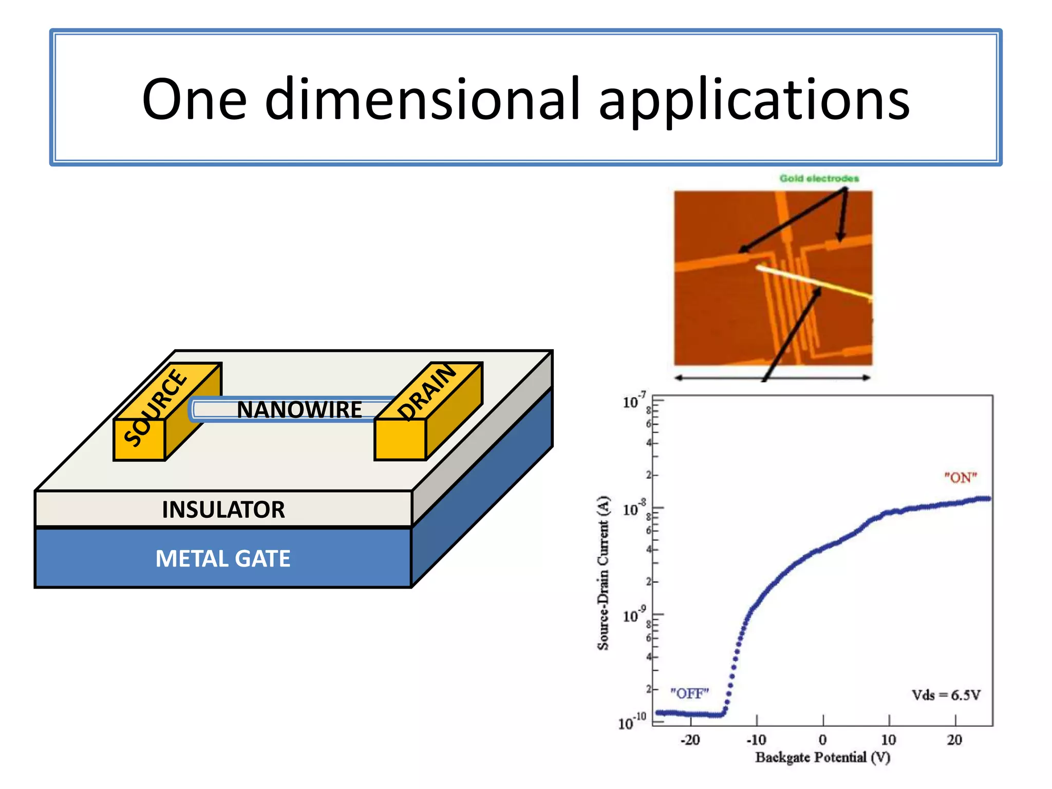
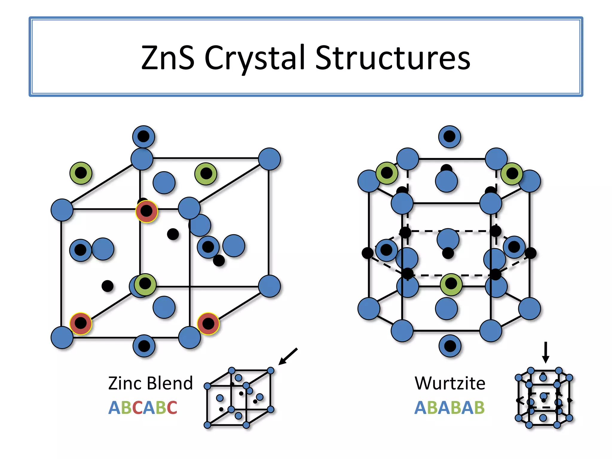
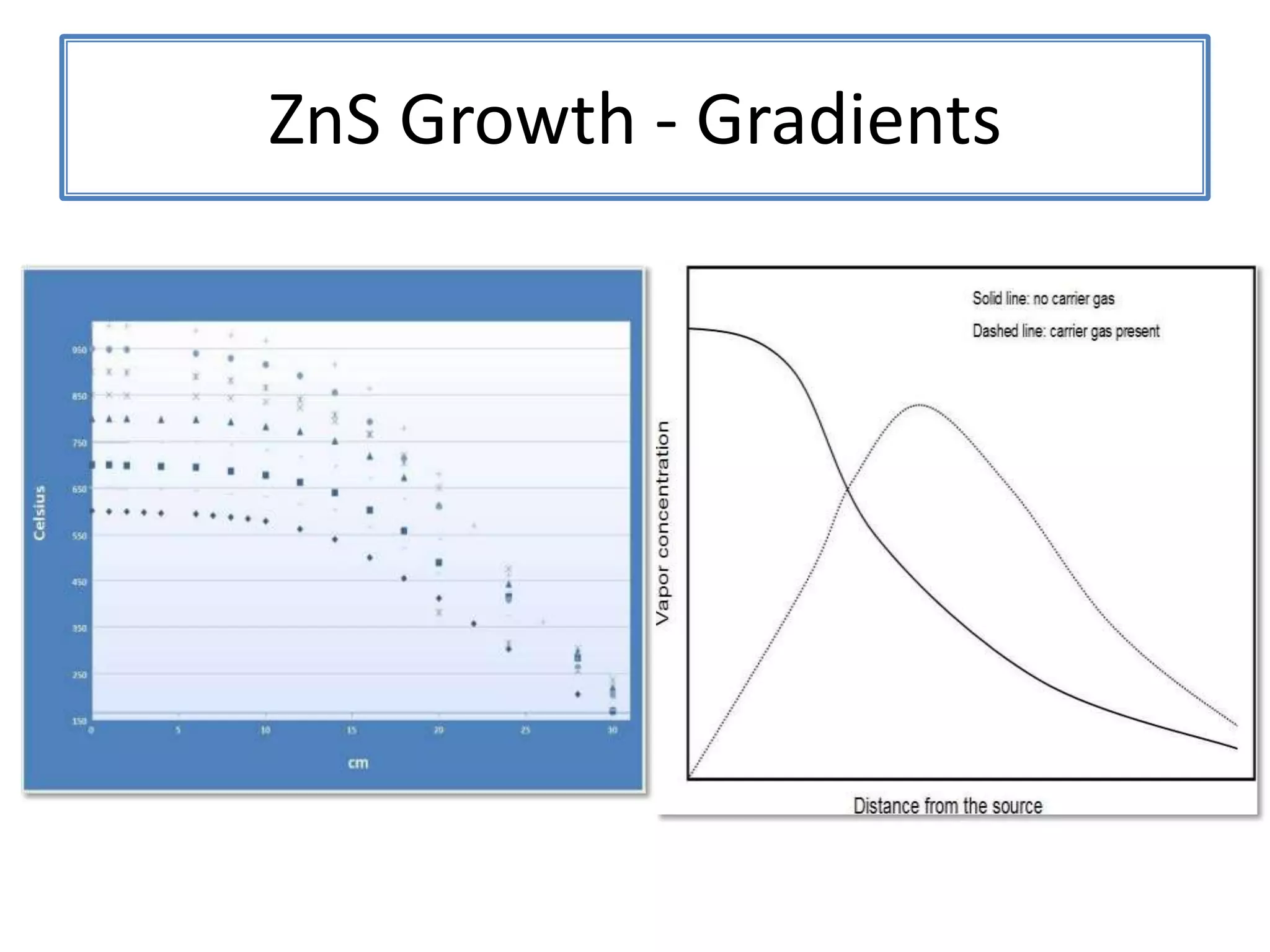
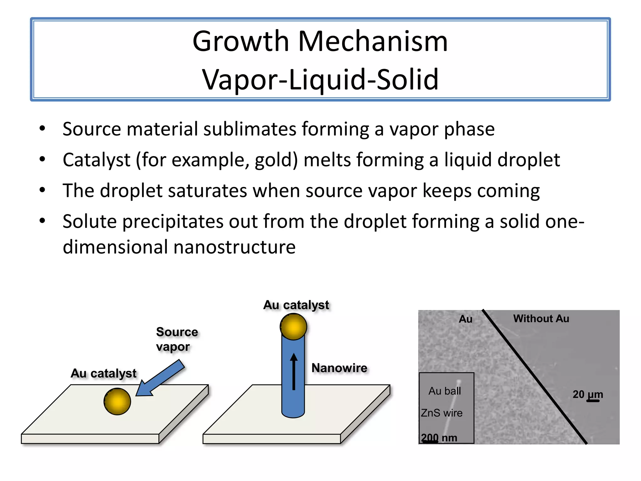
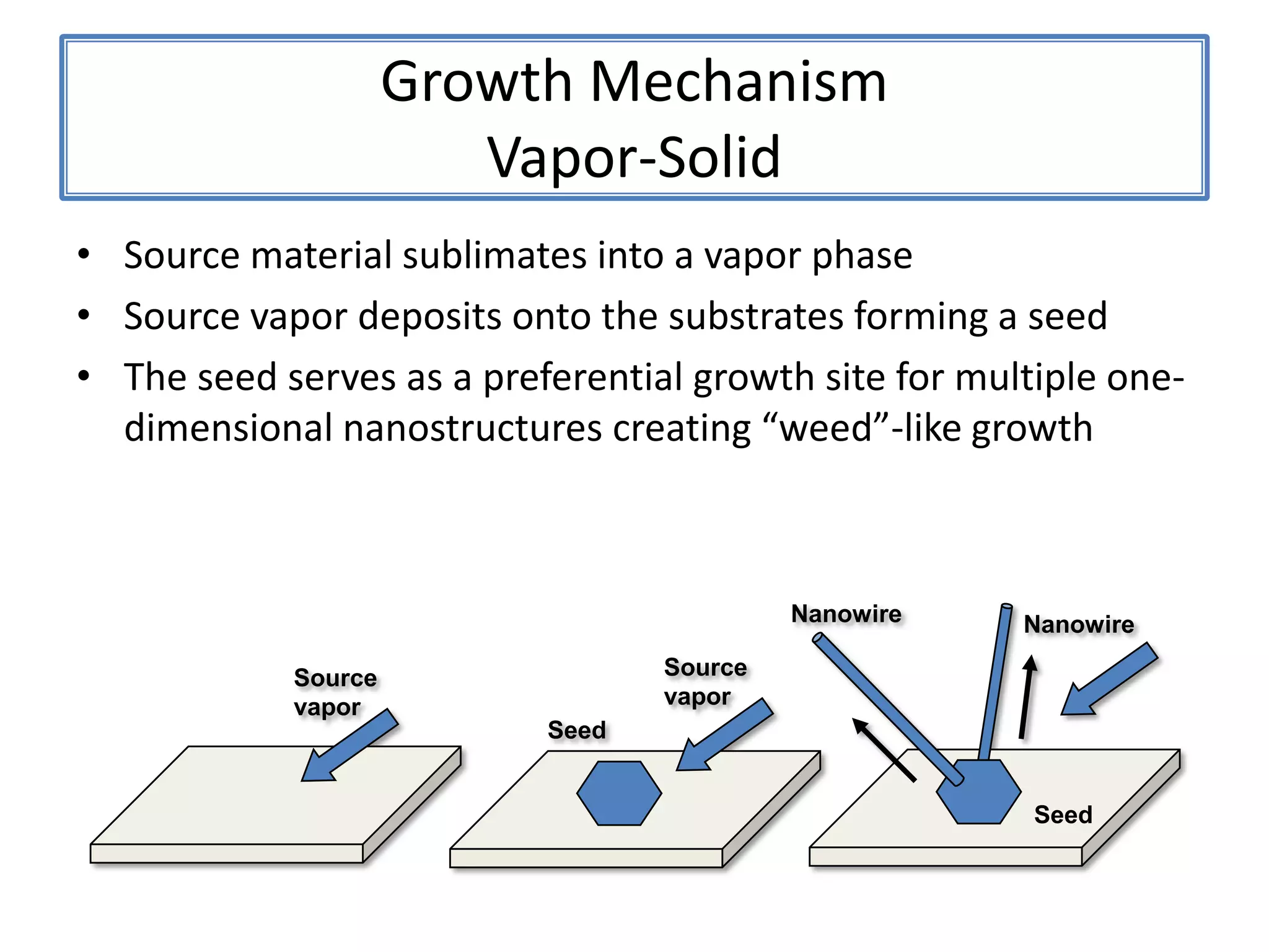
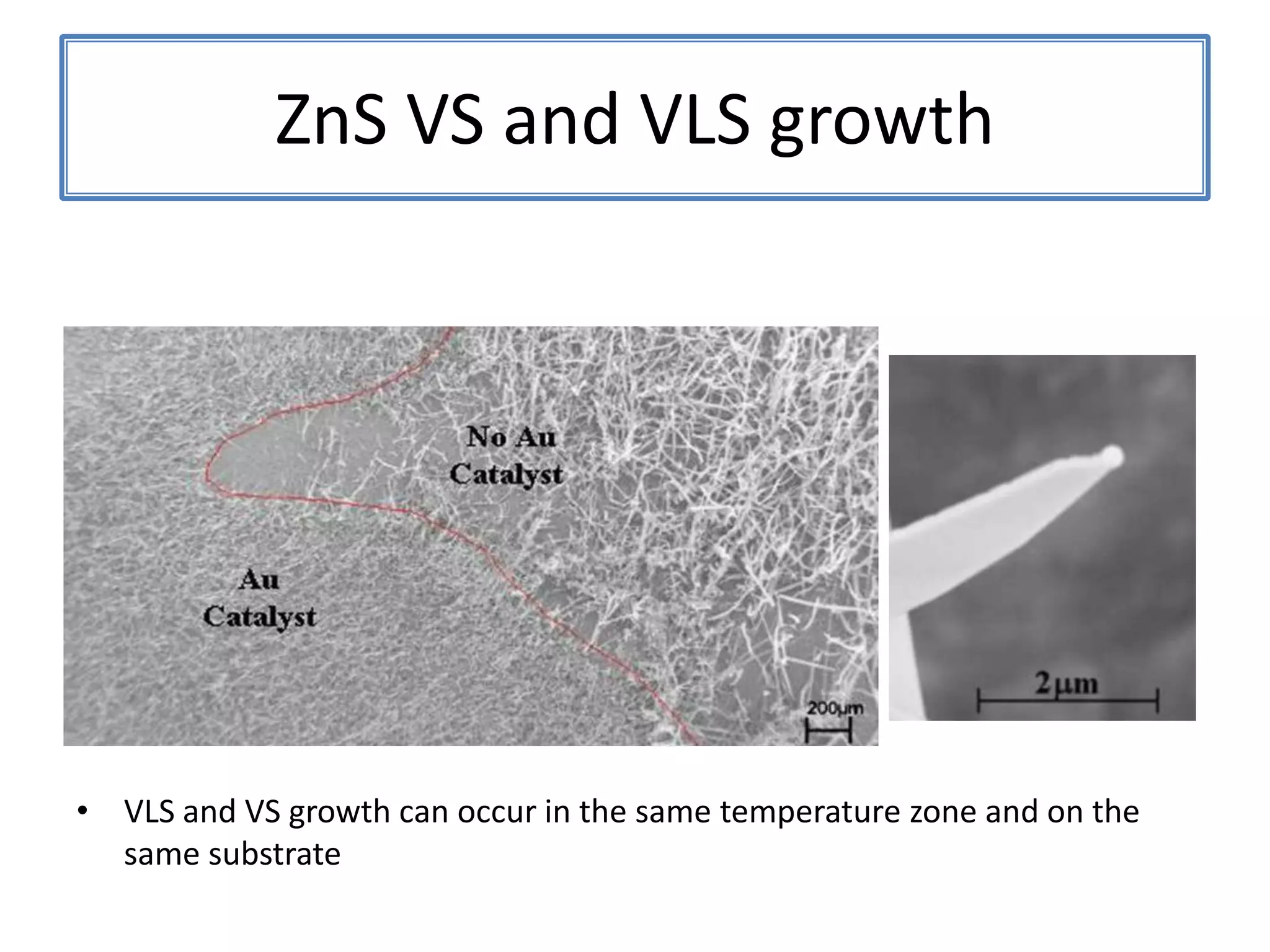
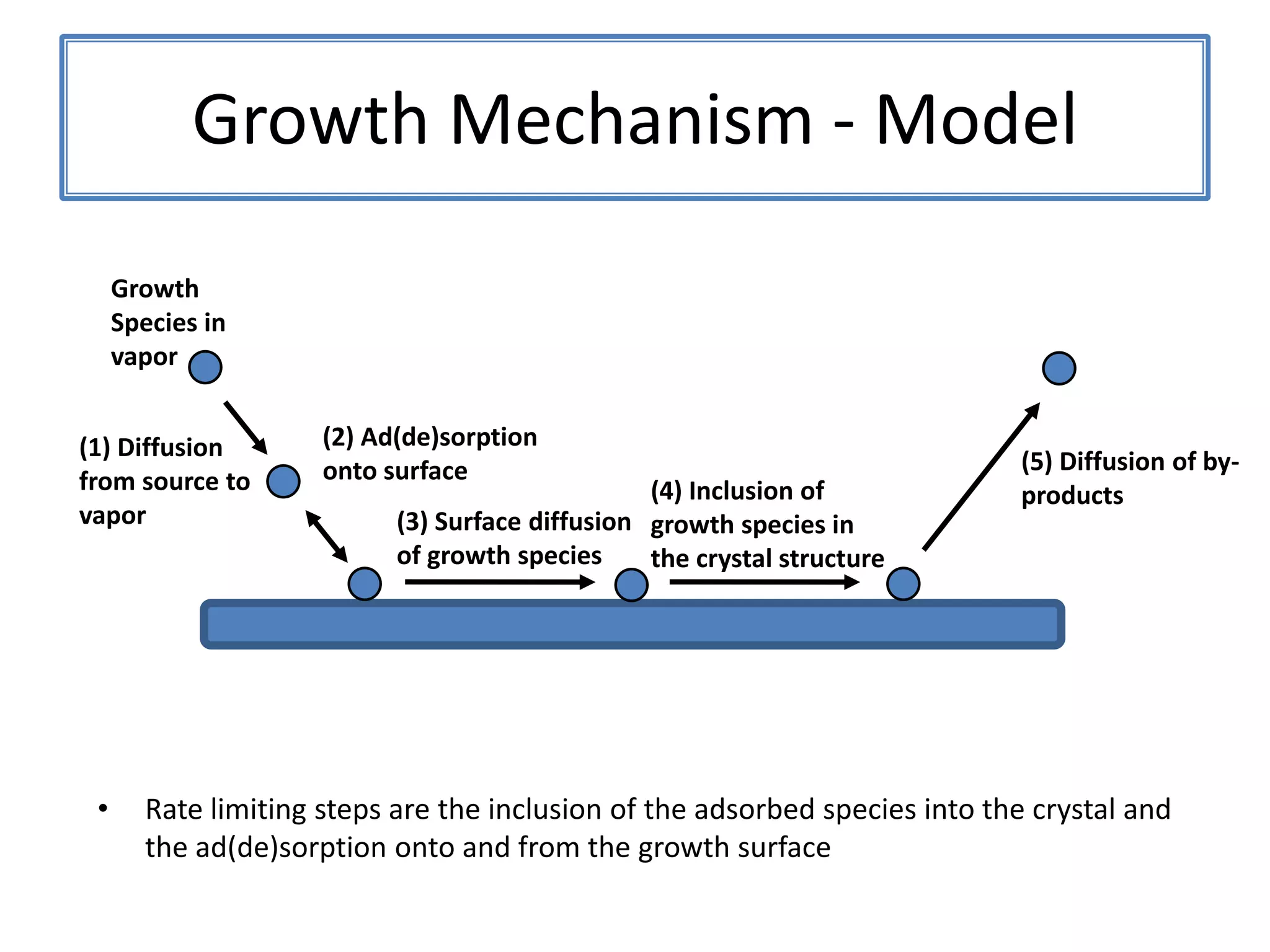
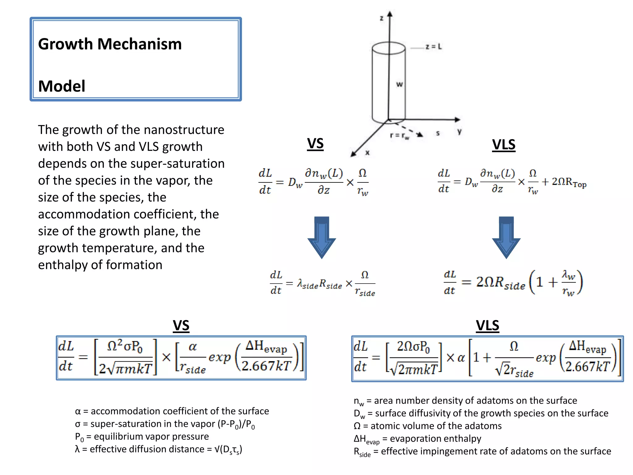
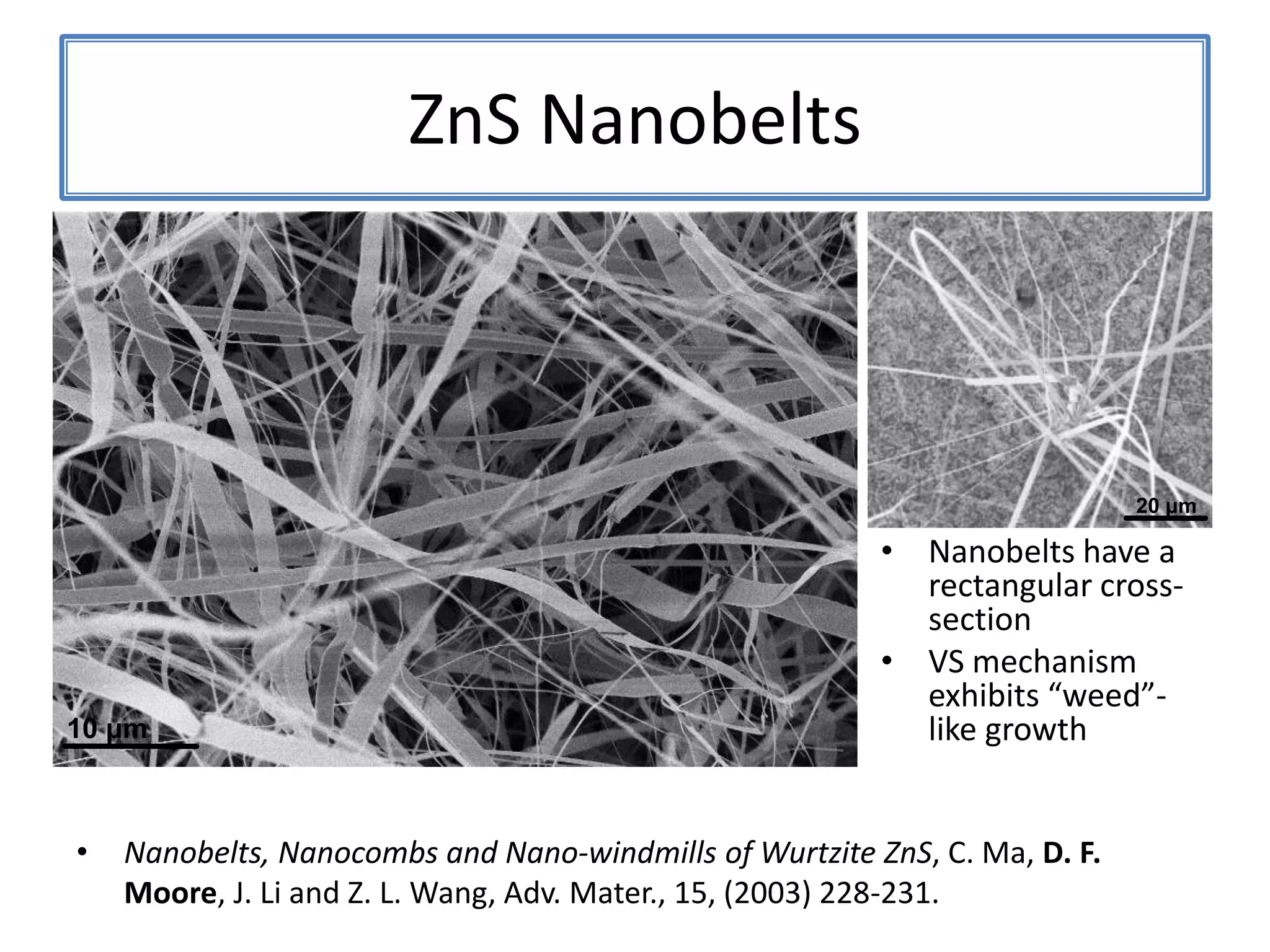
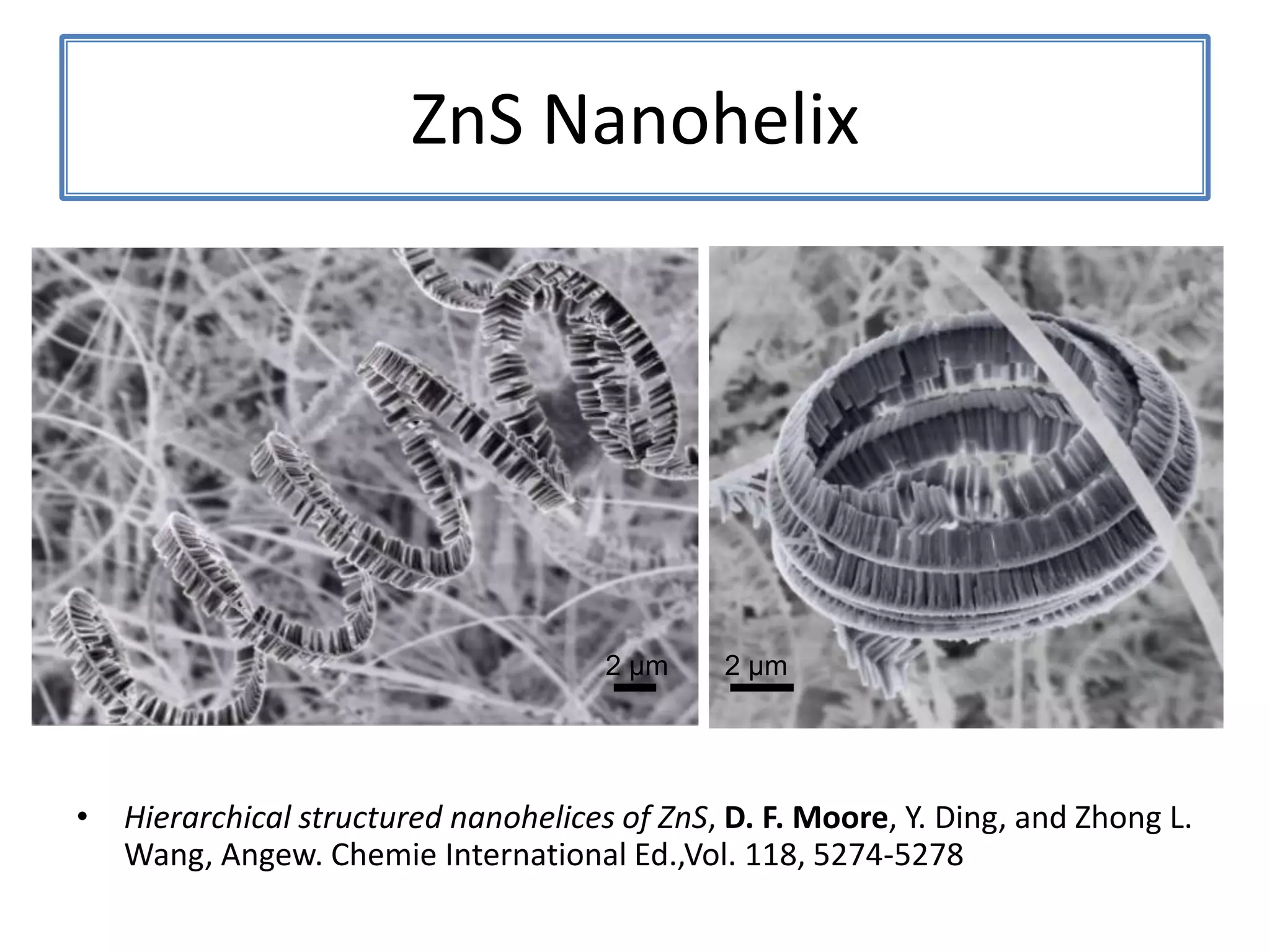
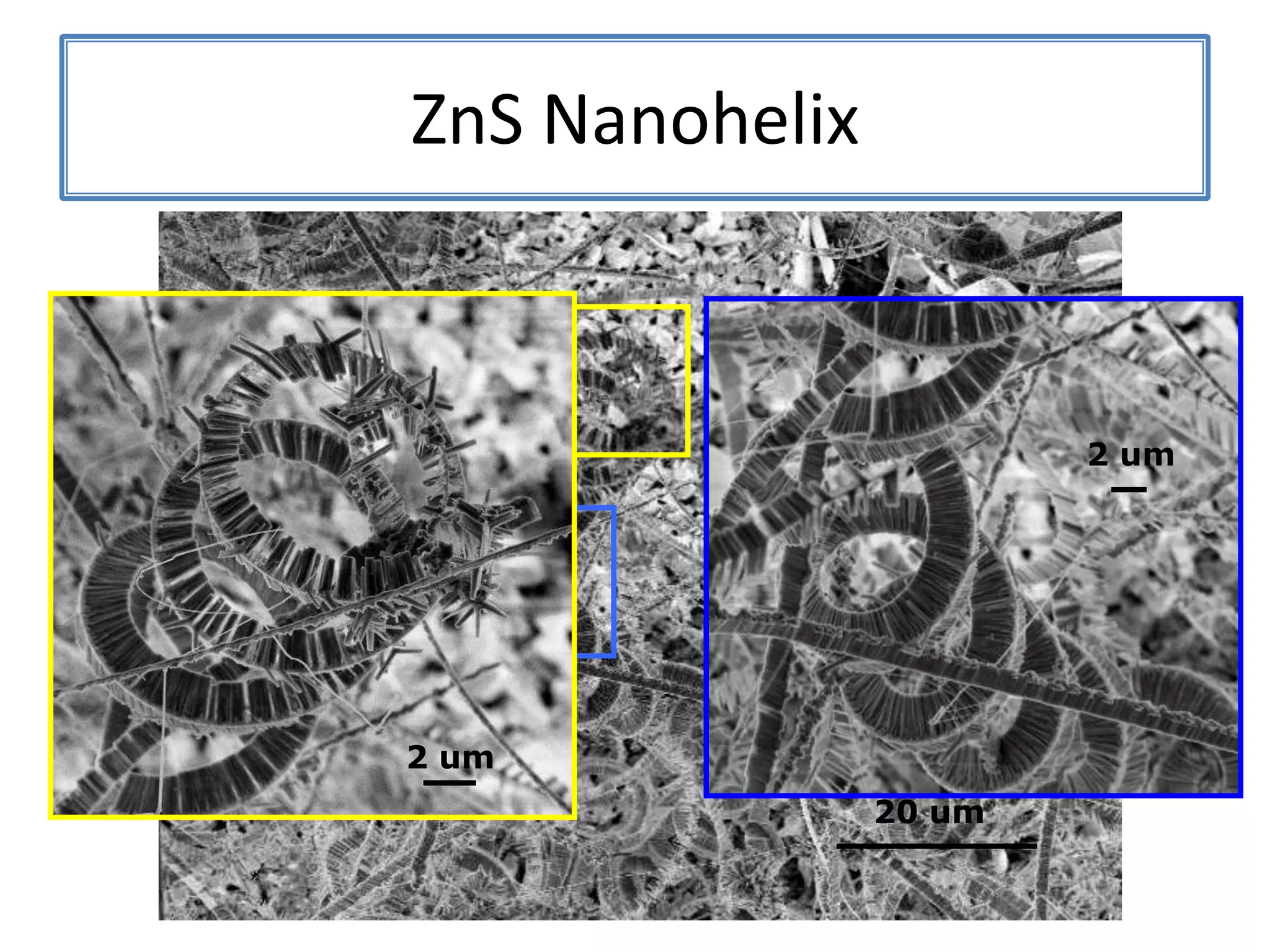
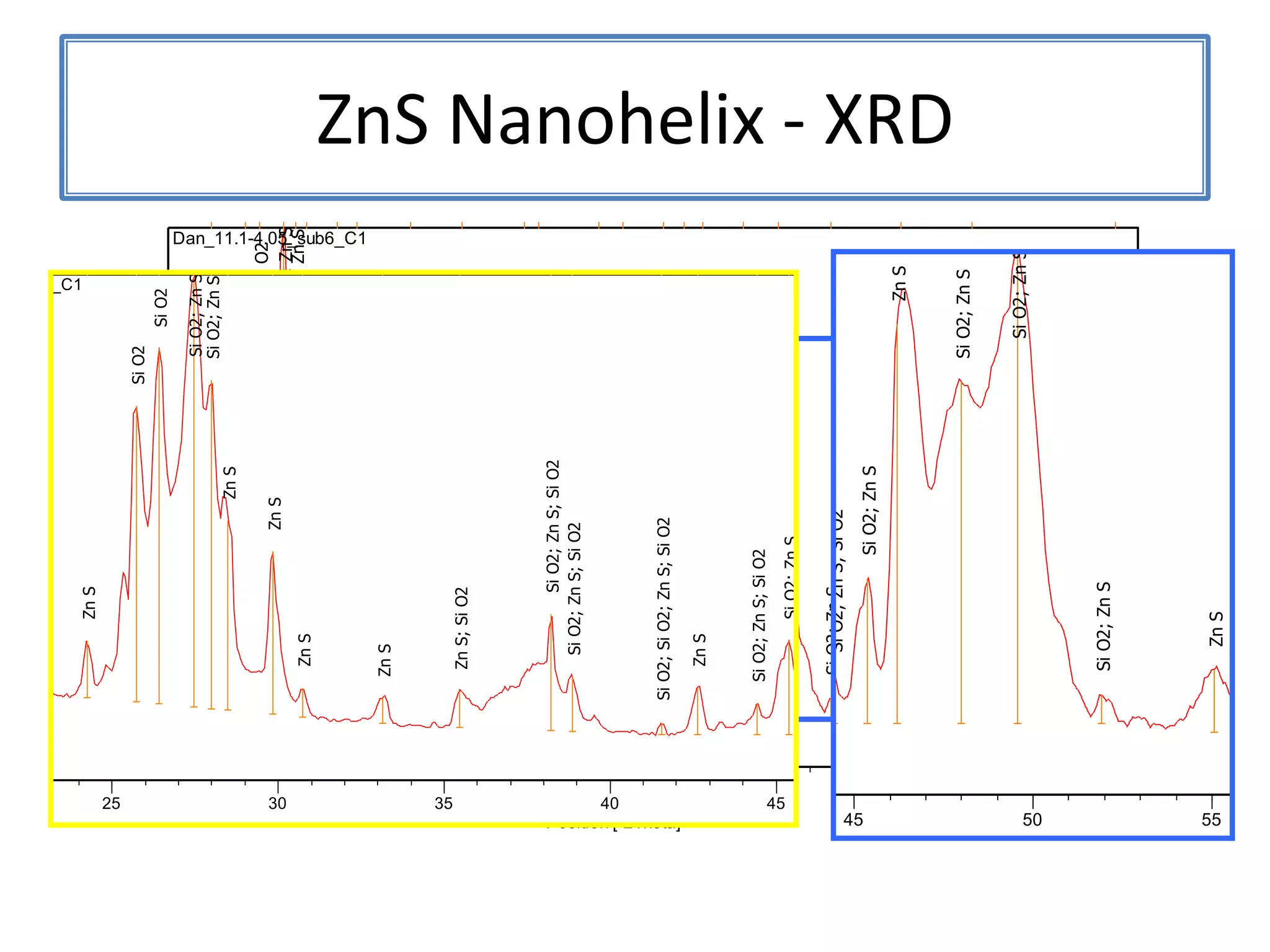
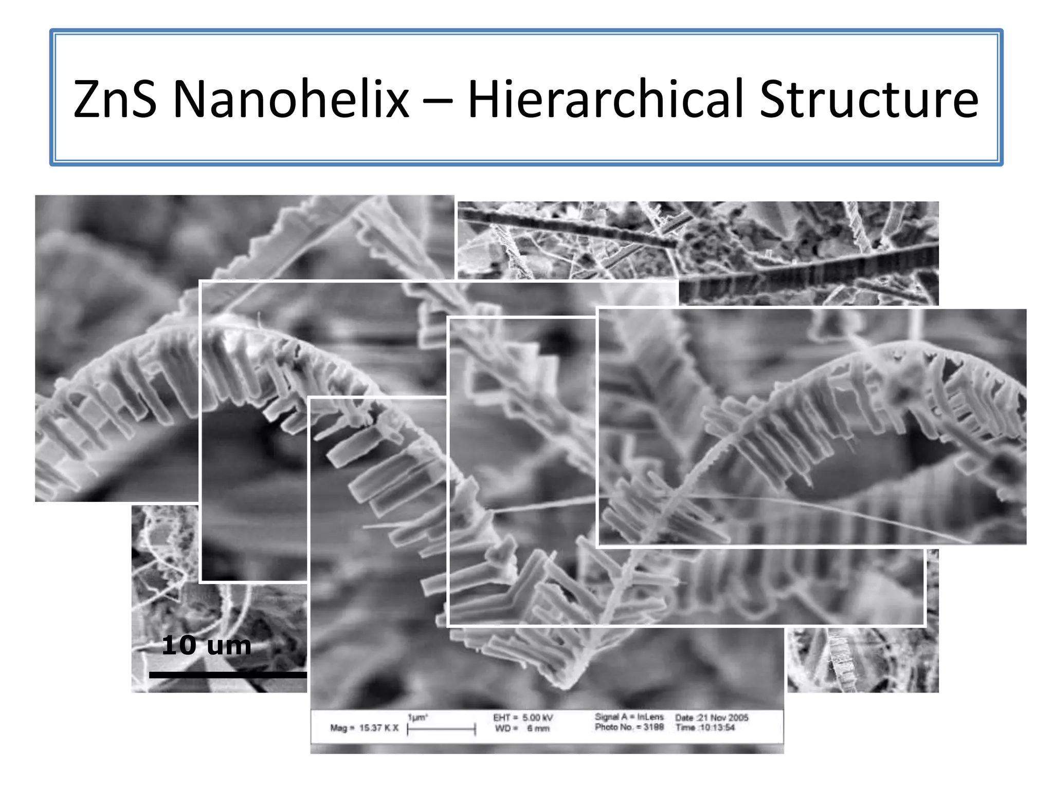
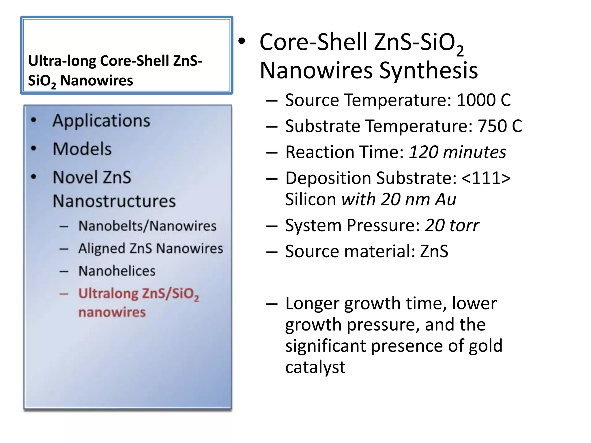
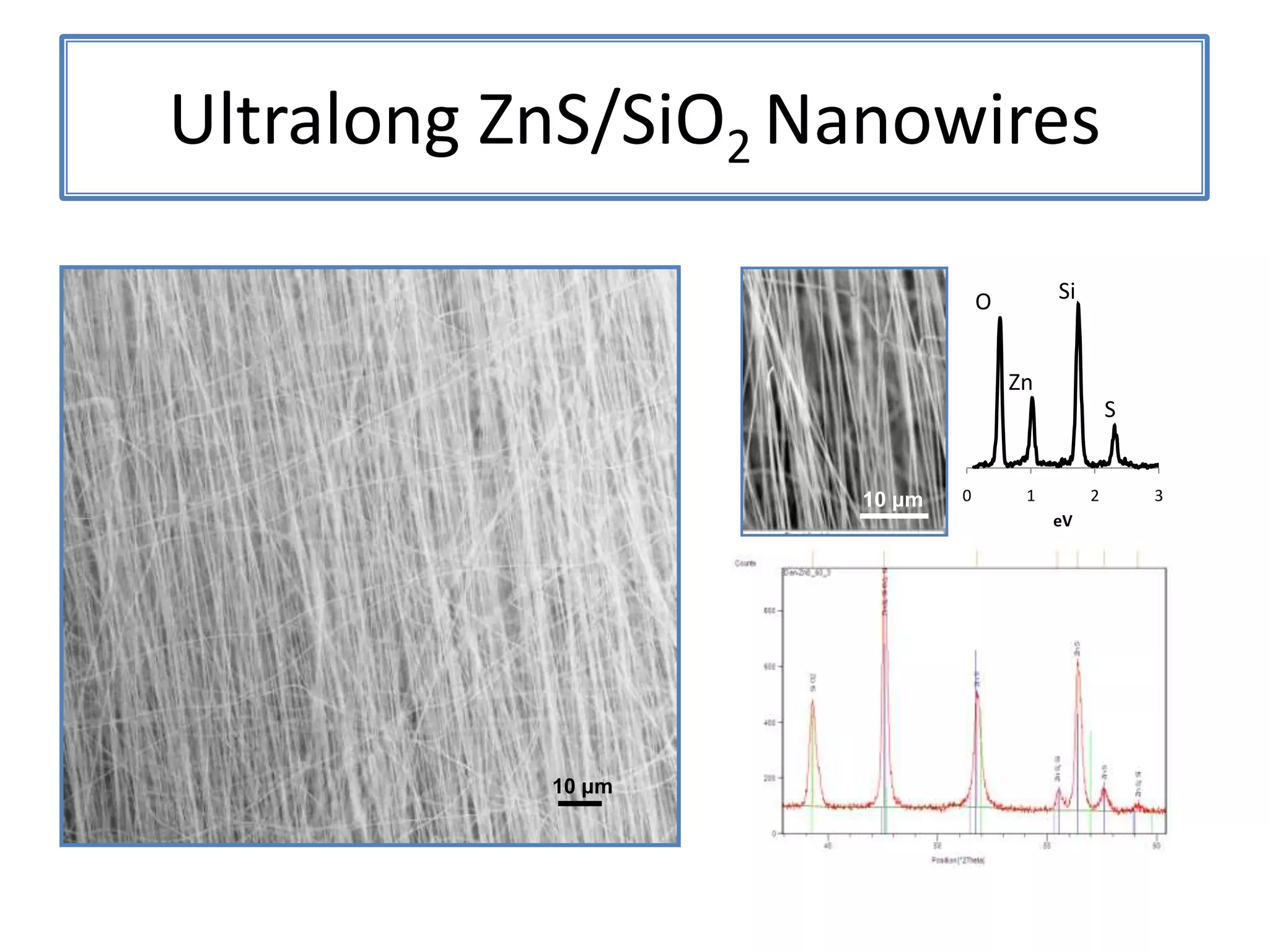
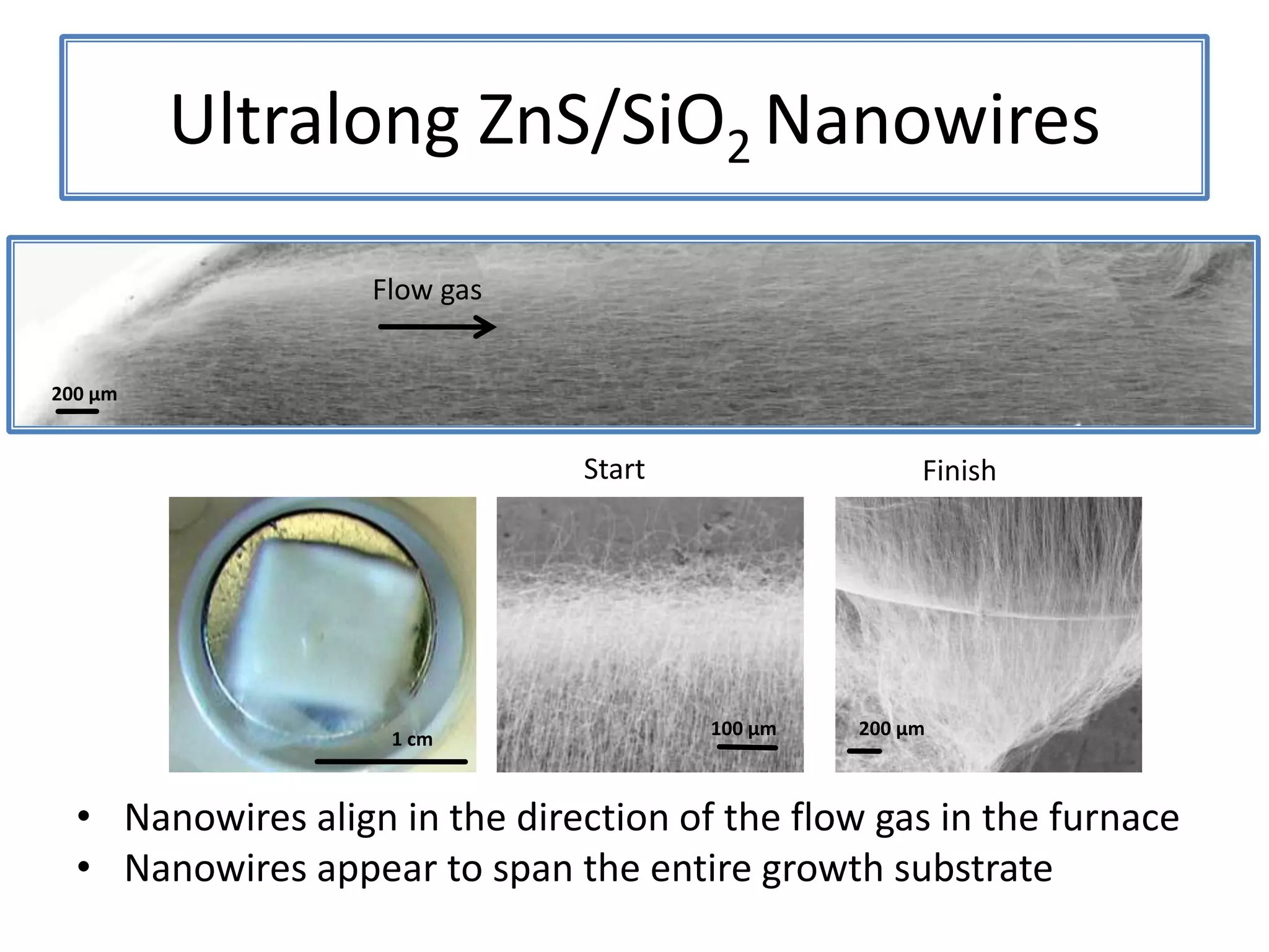
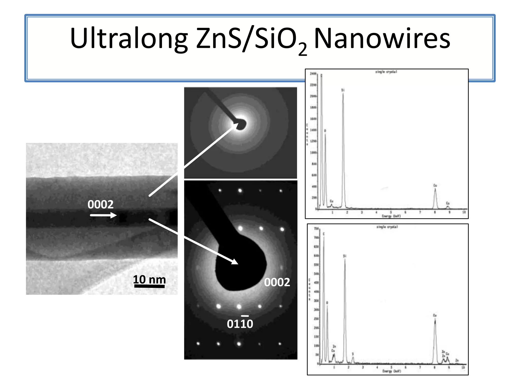
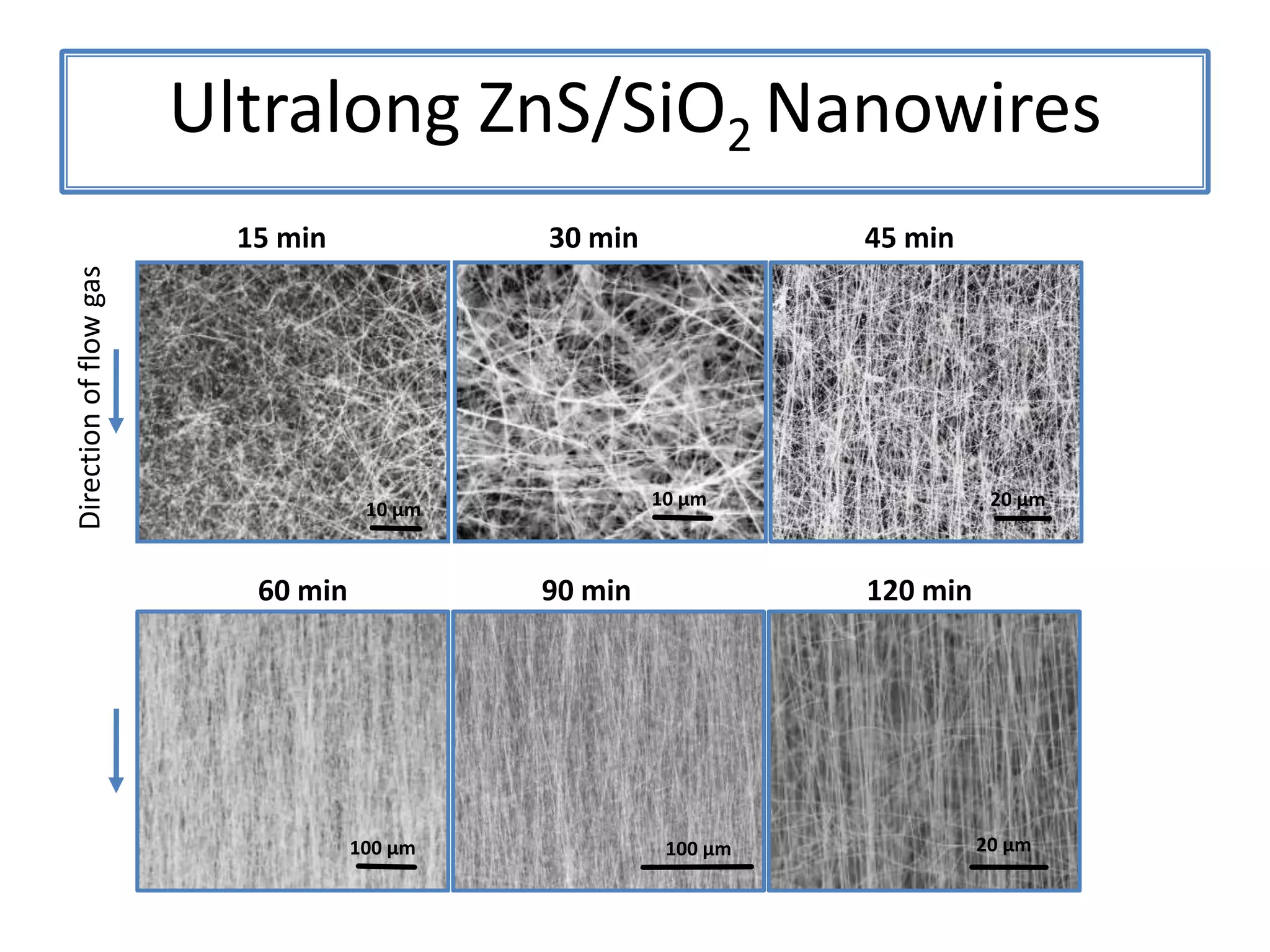
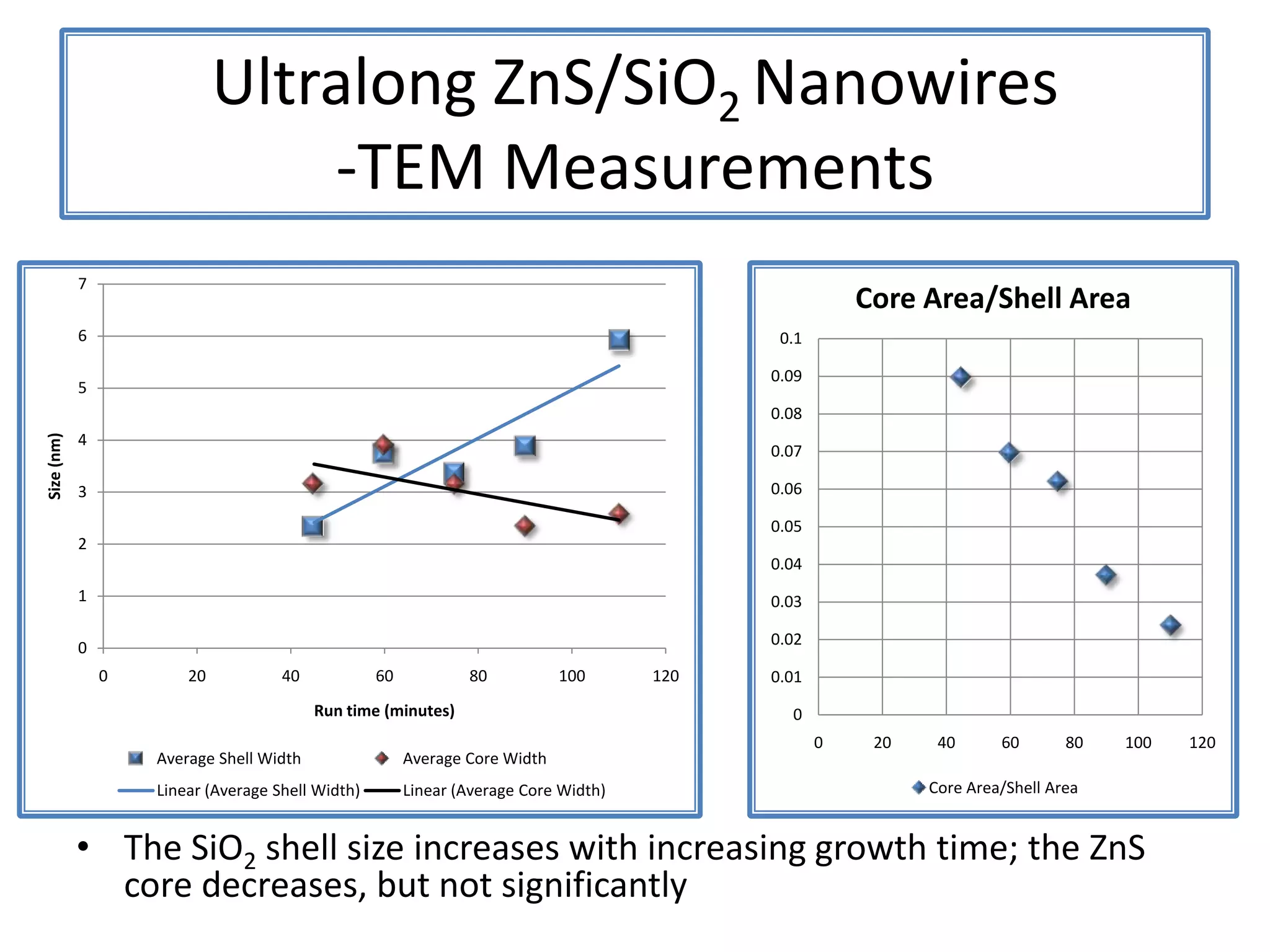
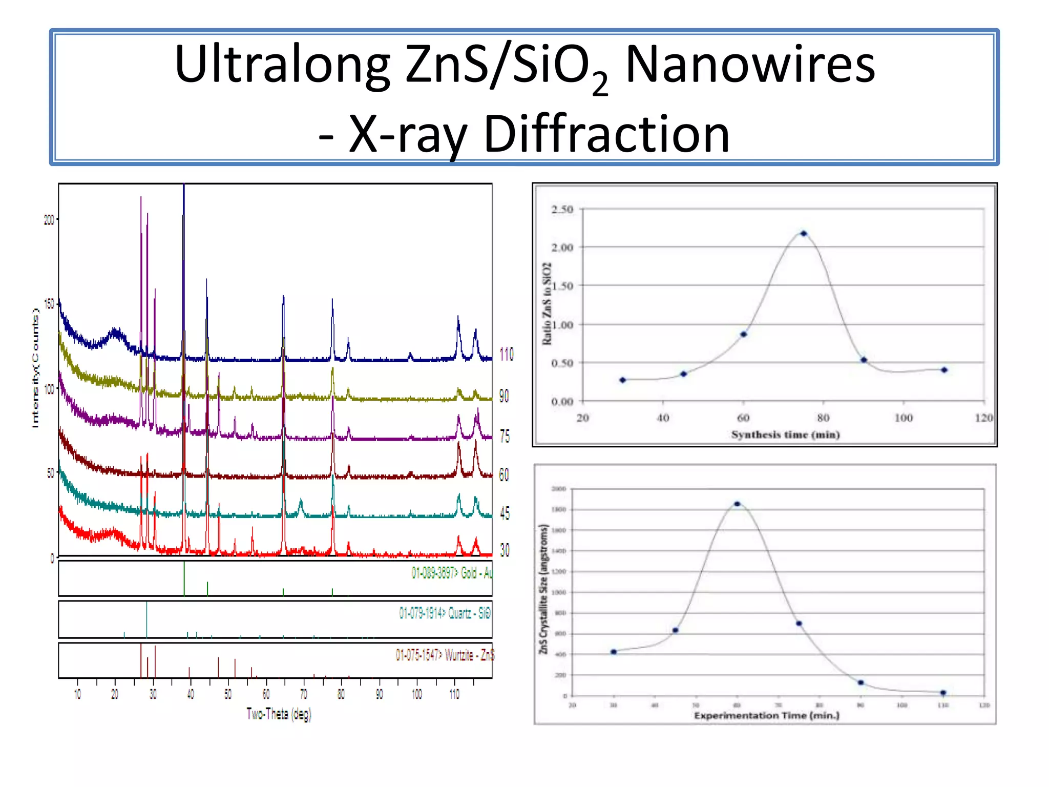
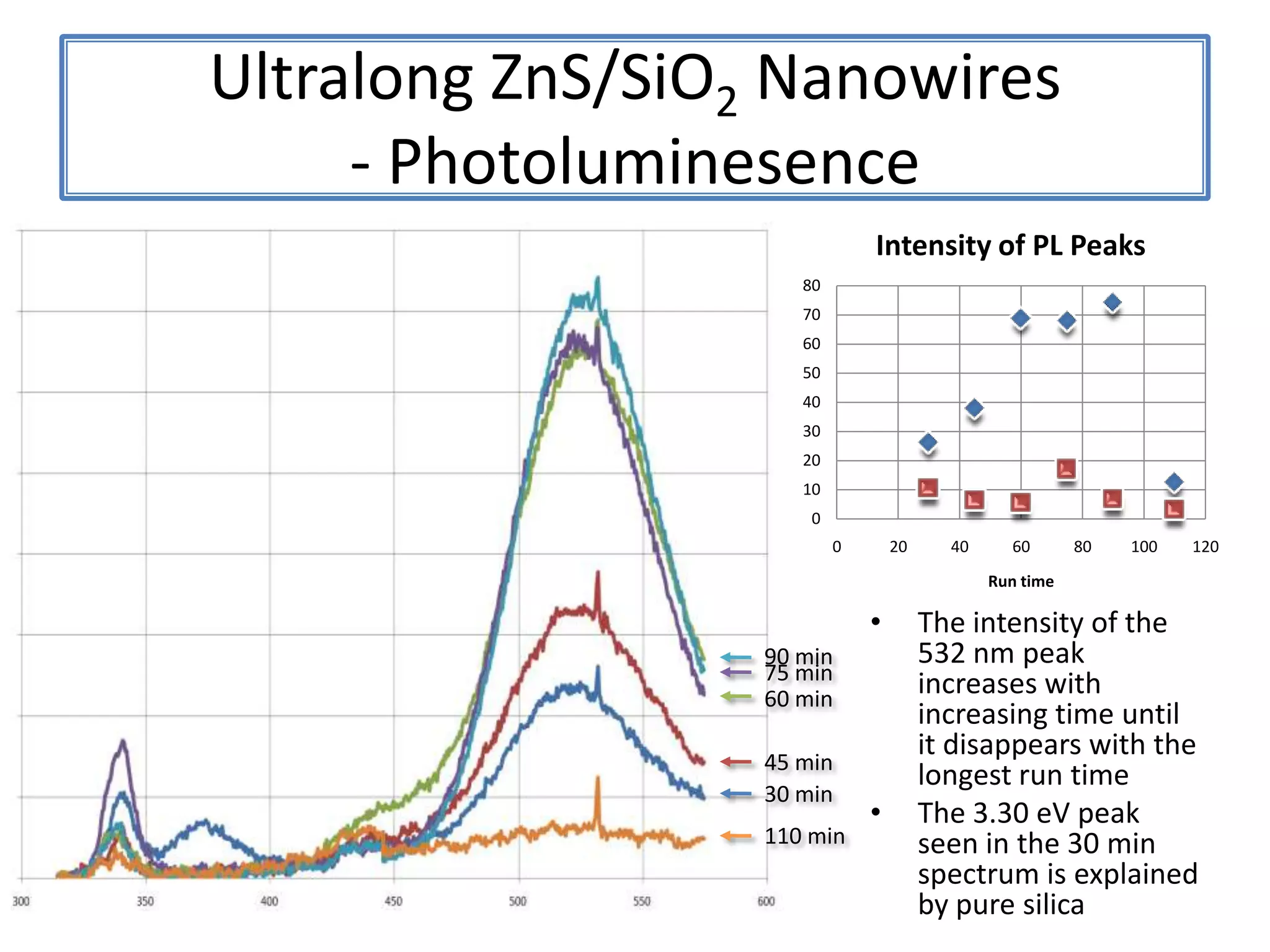
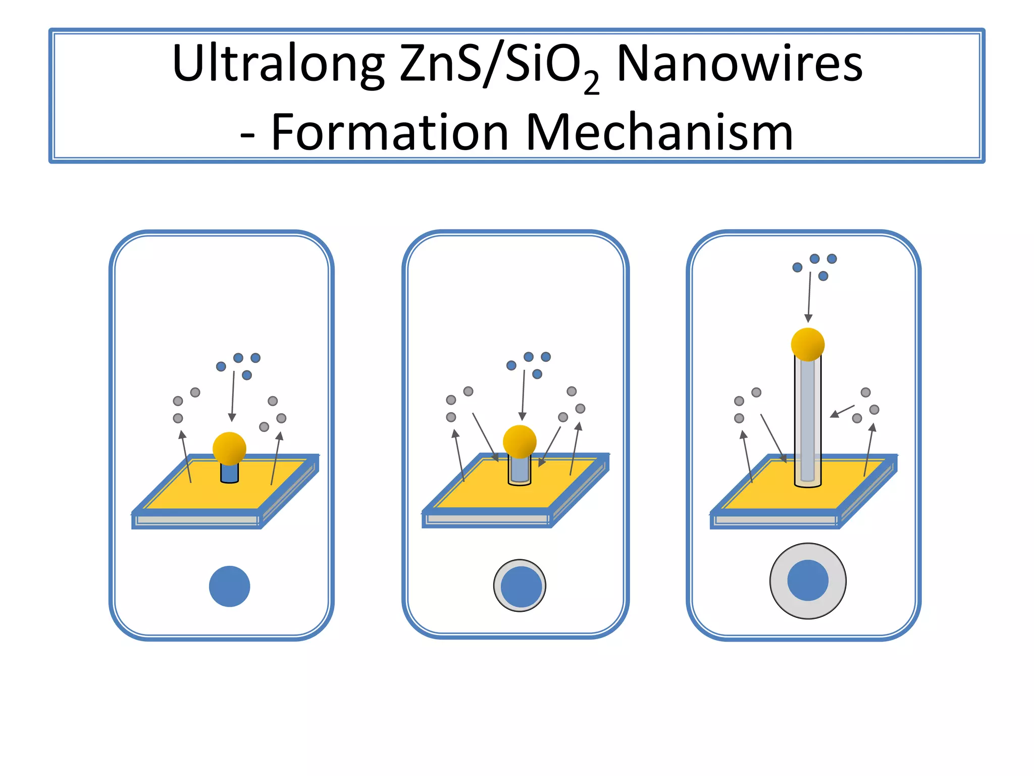
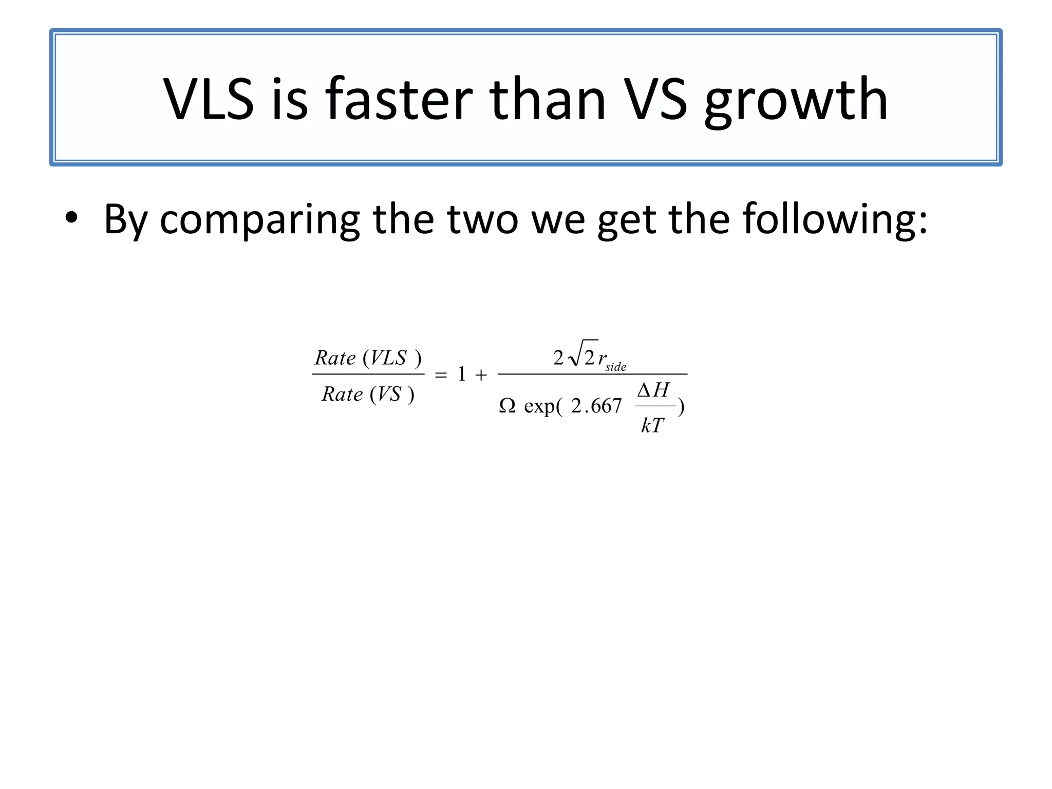
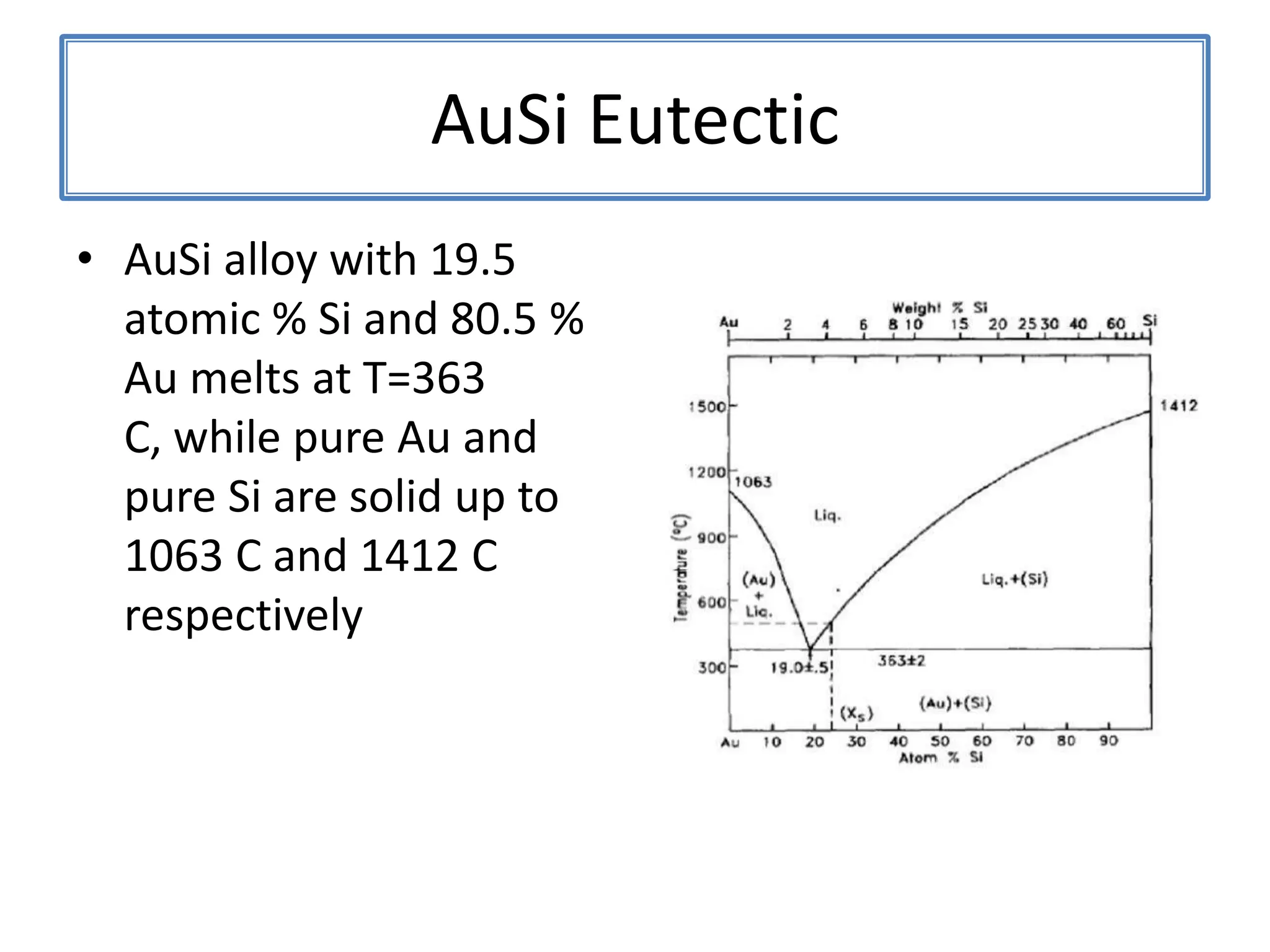
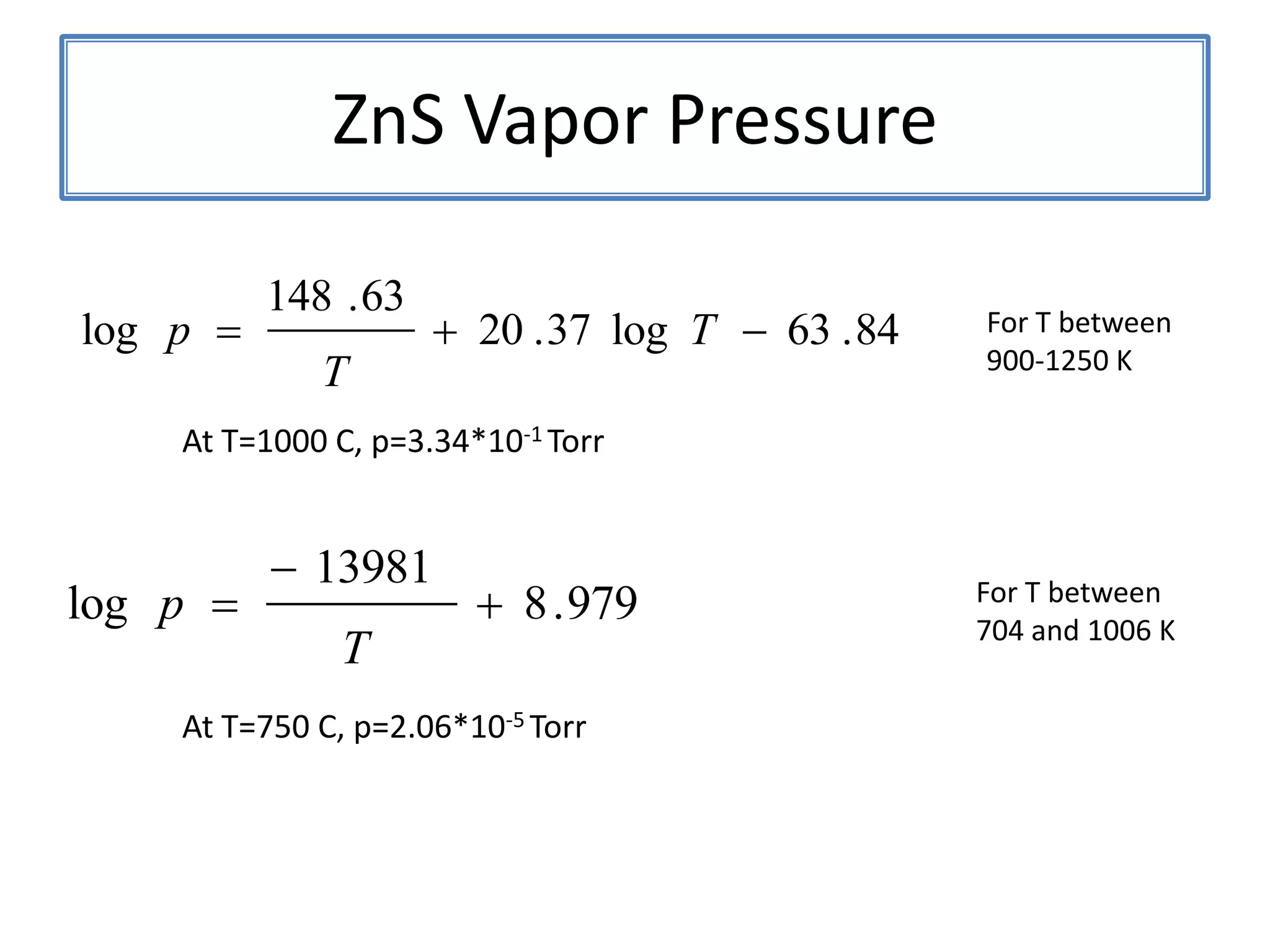
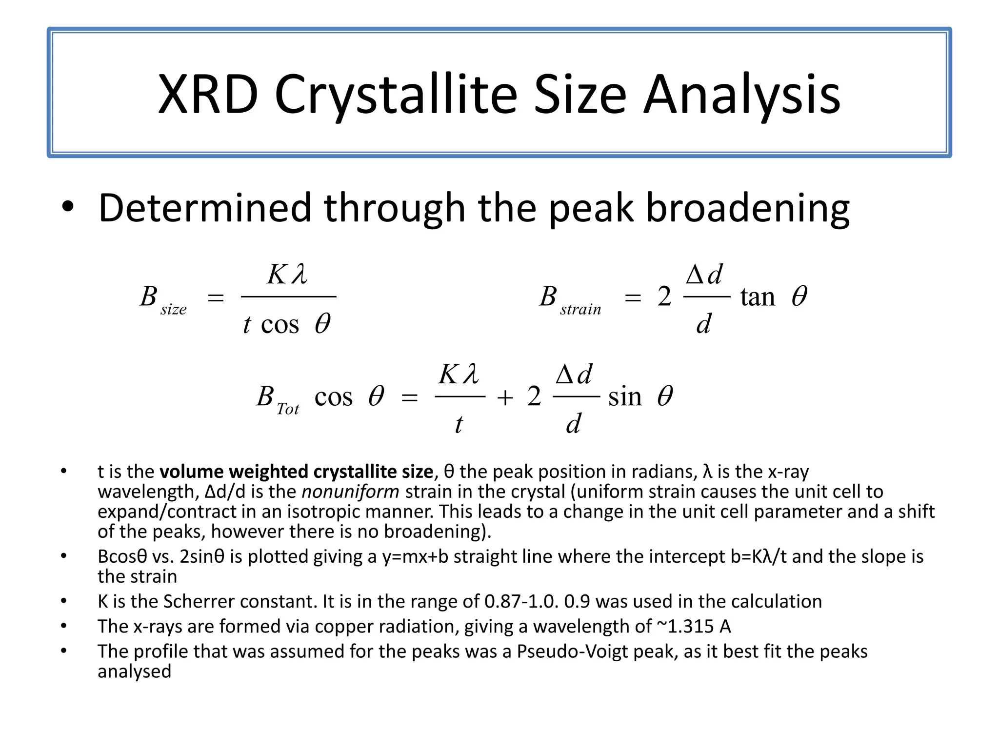
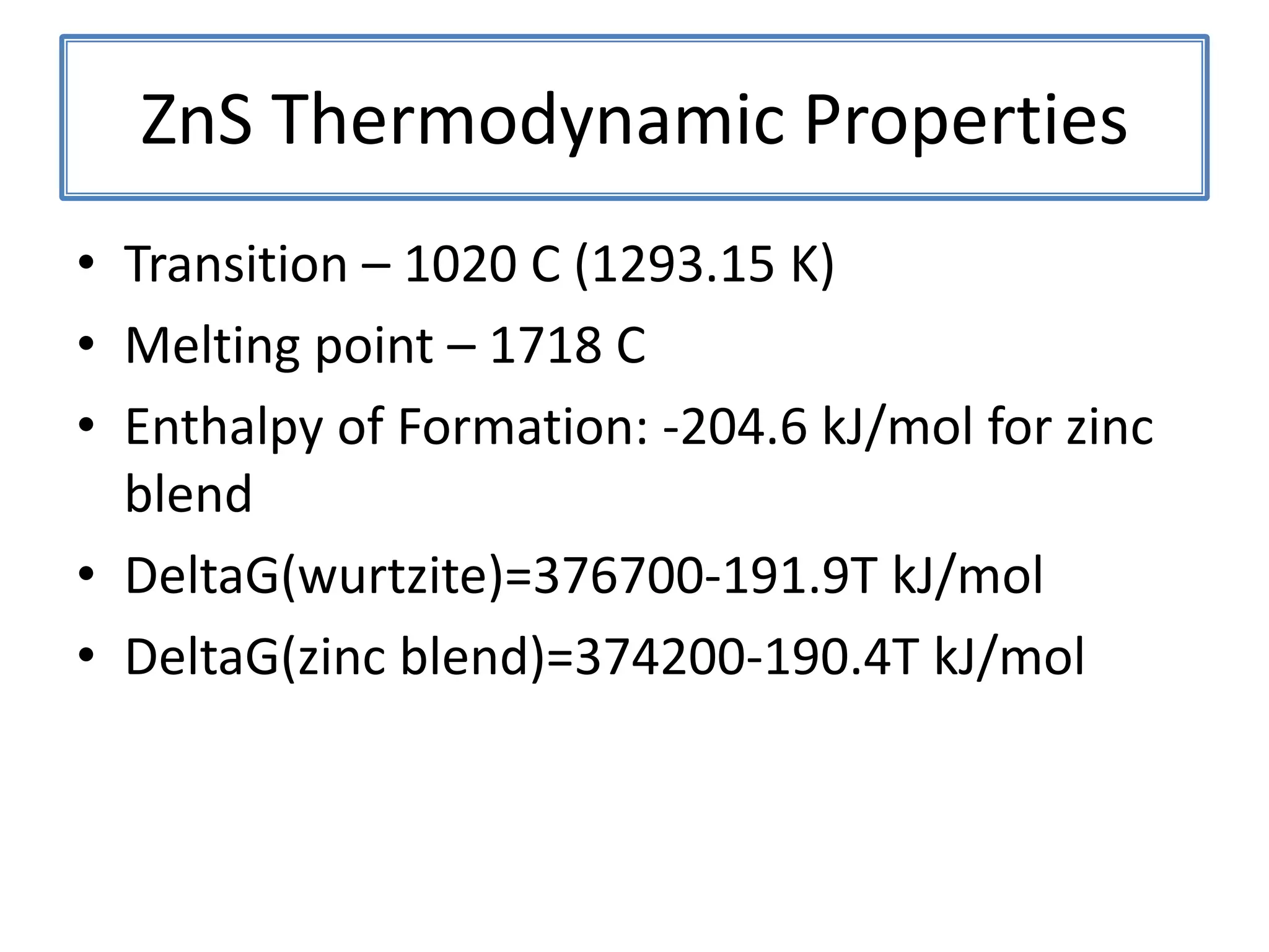
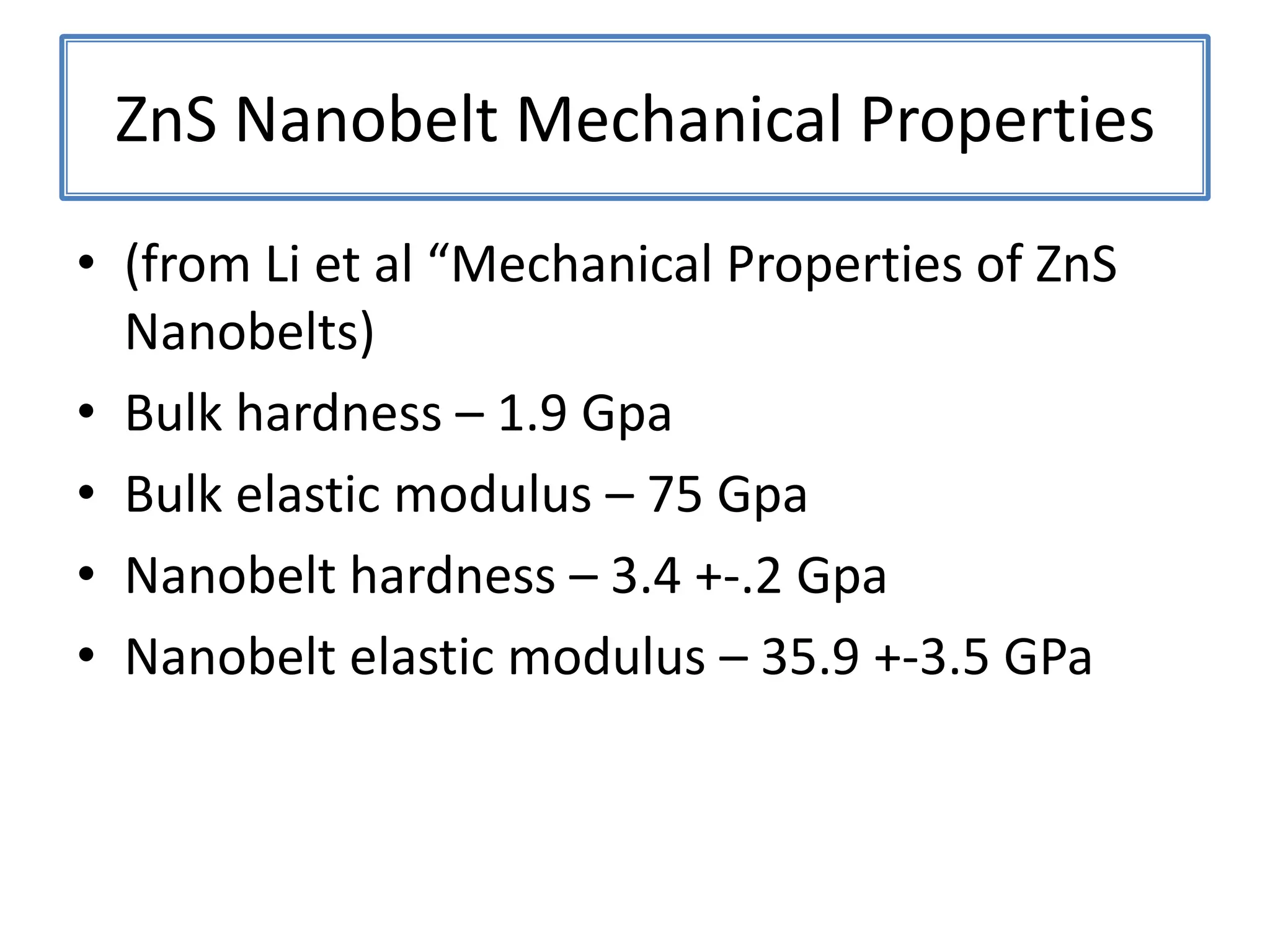
Daniel Moore's Ph.D. defense presentation summarizes his research on synthesizing and characterizing novel ZnS nanostructures. He discusses various ZnS nanostructures including nanobelts, aligned nanowires, nanohelices, and ultralong core-shell ZnS-SiO2 nanowires. Various growth mechanisms are proposed including vapor-liquid-solid and vapor-solid processes. Parameters like temperature, time, and catalyst are found to influence the morphology. Characterization using TEM, XRD and photoluminescence elucidate the crystal structure and composition of the nanostructures.
![ZnS Wurtzite(0111)(0001)Wurtzite crystal structure projected along [2110]](https://image.slidesharecdn.com/defensepresentation-090922082447-phpapp02/75/ZnS-Nanostructures-Synthesis-Characterization-and-Theory-Defense-Presentation-8-2048.jpg)
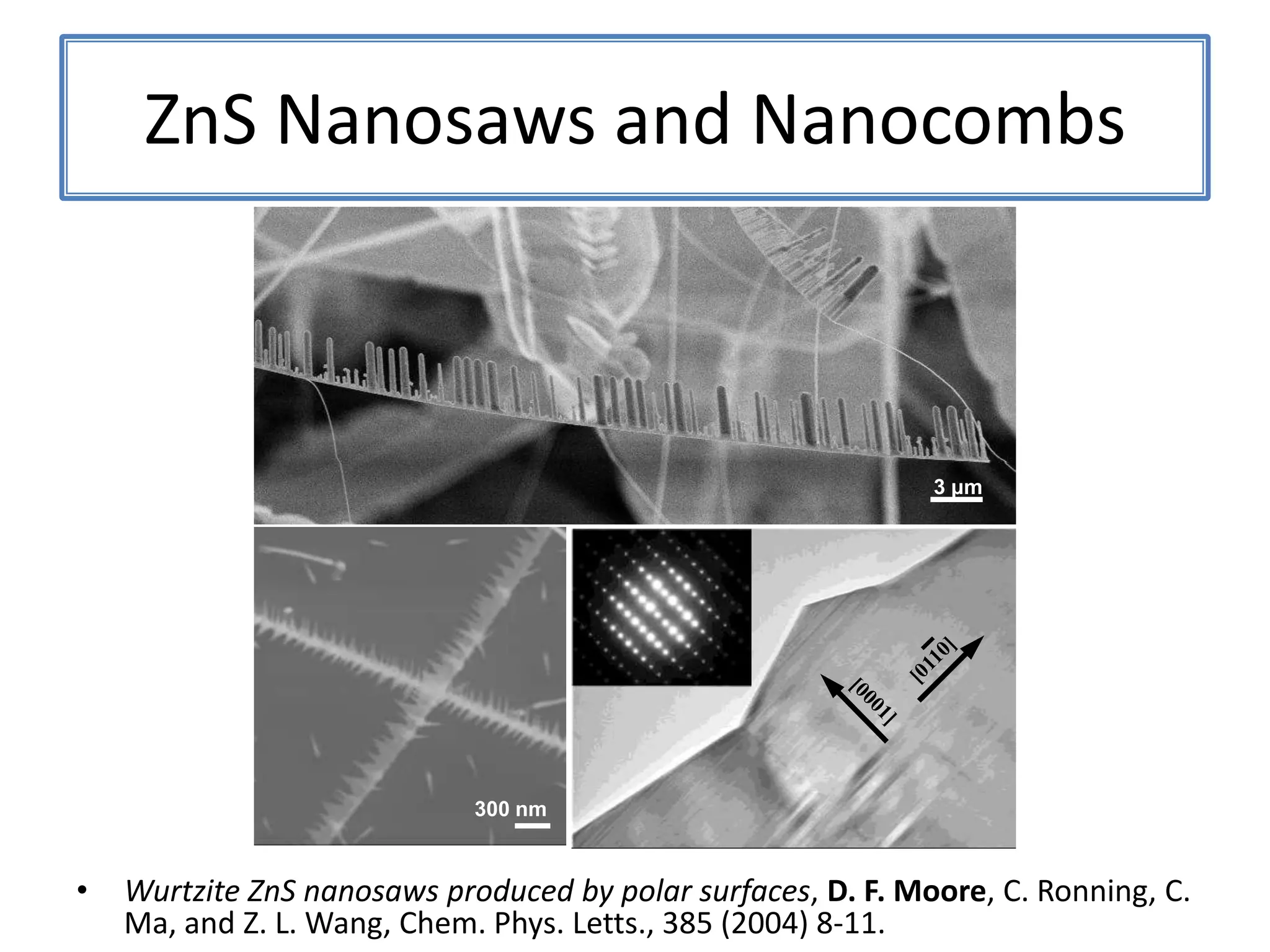
![ZnSNanosaws and Nanocombs3 μm[0110][0001]300 nmWurtzite ZnS nanosaws produced by polar surfaces, D. F. Moore, C. Ronning, C. Ma, and Z. L. Wang, Chem. Phys. Letts., 385 (2004) 8-11.](https://image.slidesharecdn.com/defensepresentation-090922082447-phpapp02/75/ZnS-Nanostructures-Synthesis-Characterization-and-Theory-Defense-Presentation-26-2048.jpg)

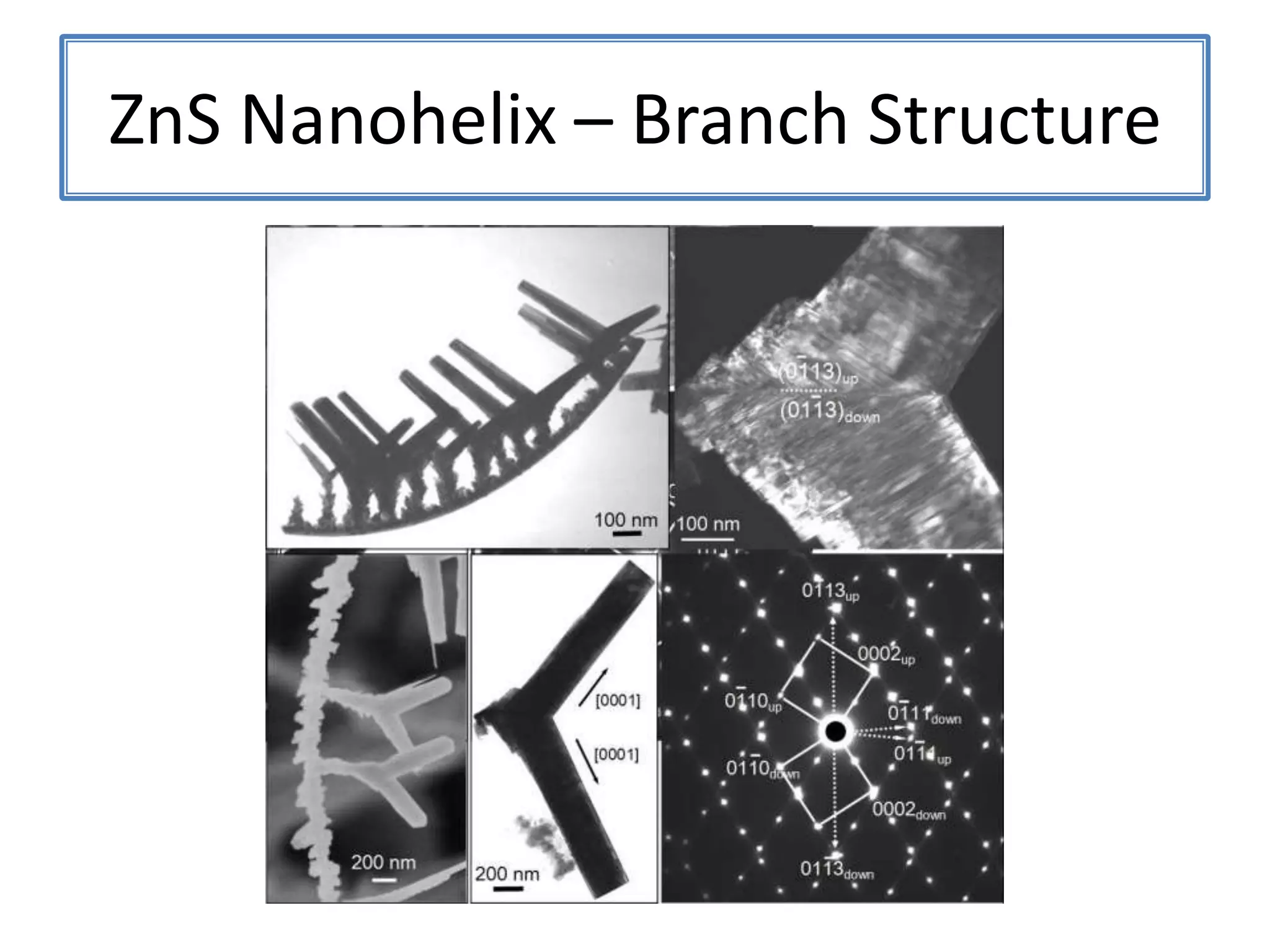
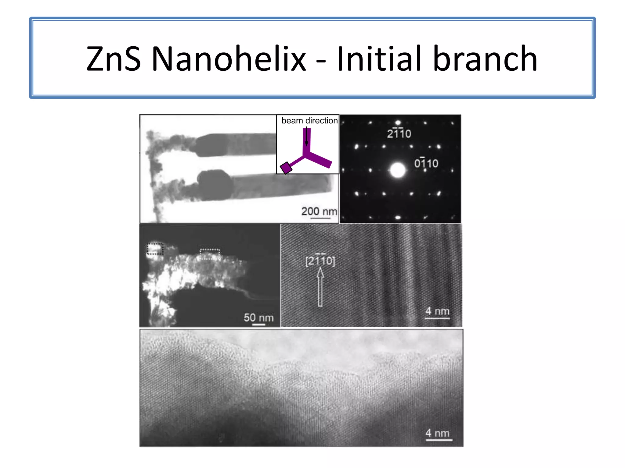
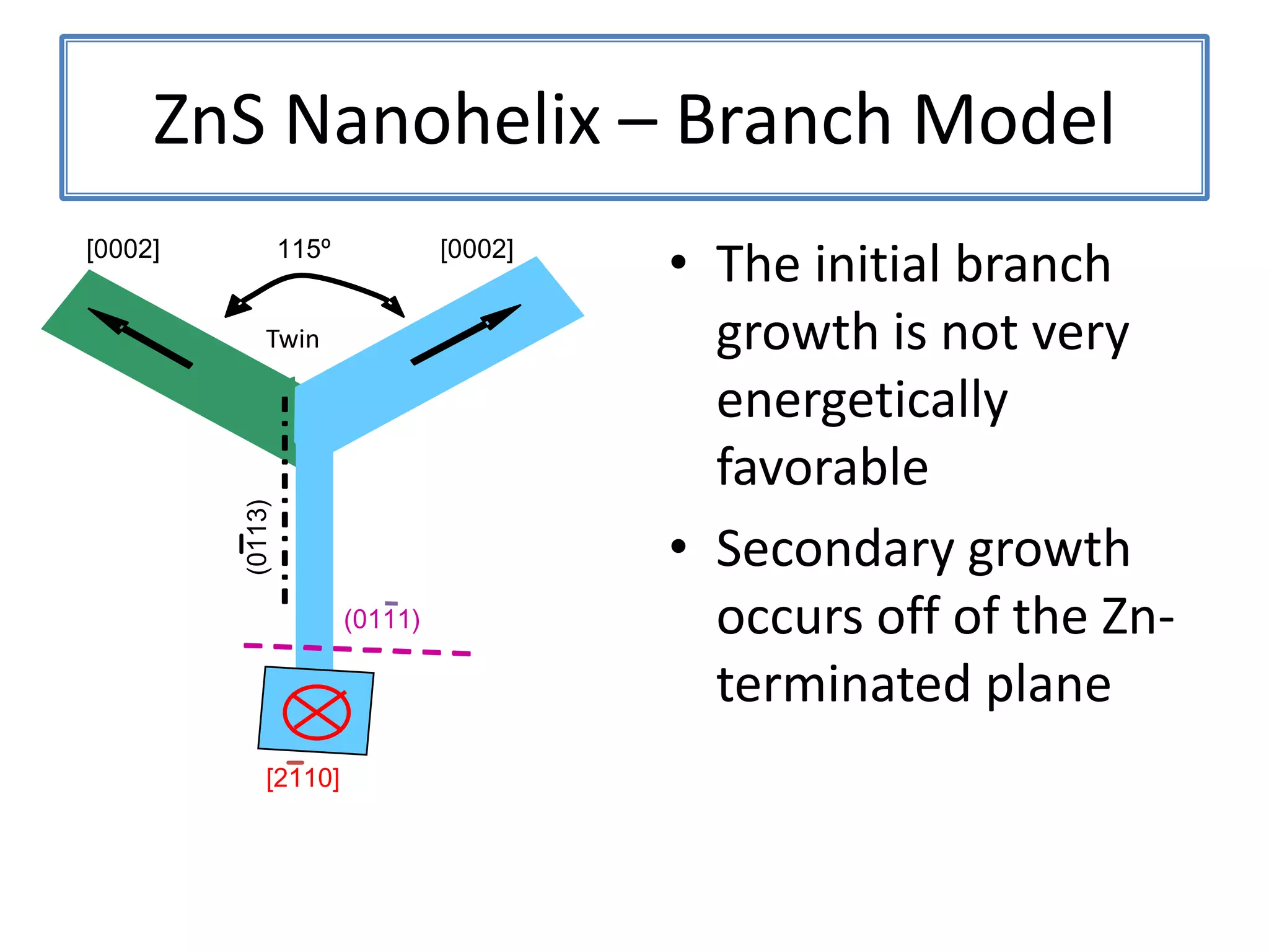

![ZnSNanohelix – Branch ModelThe initial branch growth is not very energetically favorableSecondary growth occurs off of the Zn-terminated plane[0002][0002]115ºTwin(0113)(0111)[2110]](https://image.slidesharecdn.com/defensepresentation-090922082447-phpapp02/75/ZnS-Nanostructures-Synthesis-Characterization-and-Theory-Defense-Presentation-52-2048.jpg)


![Thin_Film_Technology_introduction[1]](https://cdn.slidesharecdn.com/ss_thumbnails/1b4496c8-2102-411b-8465-a3dd3f398327-150205034538-conversion-gate02-thumbnail.jpg?width=640&height=640&fit=bounds)