
Recommended
More Related Content
What's hot
What's hot (20)
Similar to Graphene 140416111416-phpapp02
Similar to Graphene 140416111416-phpapp02 (20)
Recently uploaded
Recently uploaded (20)
Graphene 140416111416-phpapp02
- 1. Submitted by :- TUSHAR PANDAGRE EN DEPT. RCOEM,NAGPUR
- 2. Introduction Graphene, a two dimensional carbon allotrope is a highly versatile material and its amazing properties make it the strongest and lightest material due to its ability to conduct electricity and heat better than any other material. It is expected that graphene will improve the efficiency and performance of current materials and substances but in the future it will be developed along with other 2D crystals to create even more amazing compounds. Since graphene is just one atom thick other materials can be created by interjecting the graphene layers with other compounds, effectively using graphene as atomic scaffolding from which other materials are designed. The development of graphene and discovery of its exceptional properties aroused interest in other 2D crystals. High-quality graphene, though a good conductor, does not have a band gap. In order to use graphene for future nano-electronic devices it is required that it has a band gap engineered into it, which will reduce its electron mobility to that of levels currently seen in strained silicone films.
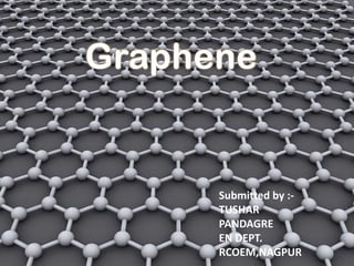
- 4. • It is almost completely transparent, yet so dense that not even helium can pass through it. • It is the one-atom thick planar sheet of carbon atoms (graphite), which makes it the thinnest material ever discovered. • 2-dimentional crystalline allotrope of carbon. • C-C Bond length is 0.142 nm. • Graphene Sheets interplanar spacing is of 0.335 nm. STRUCTURE
- 5. Graphene can self-repair holes in its sheets, when exposed to molecules containing carbon, such as hydrocarbons. Bombarded with pure carbon atoms, the atoms perfectly align into hexagons, completely filling the holes. STRUCTURAL PROPERTIES OF GRAPHENE
- 6. • Graphene one atom thick are a hundred times more chemically reactive than thicker sheets. (Stanford university) • Graphene is chemically the most reactive form of carbon. CHEMICAL ELECTRONIC • Intrinsic graphene is a semi-metal or zero-gap semiconductor. ELECTRICAL •Graphene has a remarkably high electron mobility at room temperature, with reported values in excess of 15000 cm2·V−1·s−1 •It conducts electricity as efficiently as copper and outperforms all other materials as a conductor of heat.
- 7. • One-atom-thick crystal can be seen with the naked eye because it absorbs approximately 2.3% of white light. • Graphene's unique optical properties produce an unexpectedly high opacity for an atomic monolayer in vacuum OPTICAL inch scale graphene film on Stretchable SubstrateTHERMAL Thermal conductivity is measured to be between (4.84±0.44) × 103 to (5.30±0.48) × 103 W·m−1·K−1
- 8. • The flat graphene sheet is unstable with respect to scrolling i.E. Bending into a cylindrical shape. • Graphene appeared to be one of the strongest materials known with a breaking strength over 100 times greater than a hypothetical steel film of the same (thin) thickness, with a young's modulus (stiffness) of 1 tpa (150000000 psi). MECHANICAL
- 9. 1.MECHANICAL EXFOLIATION : This involves splitting single layers of graphene from multi-layered graphite. Achieving single layers typically requires multiple exfoliation steps, each producing a slice with fewer layers, until only one remains. Geim and Novosolev used adhesive tape to split the layers. SOME PRODUCTION METHODS 2. EPITAXY : Epitaxy refers to the deposition of a crystalline overlayer on a crystalline substrate and the graphene–substrate interaction can be further passivated •In some cases epitaxial graphene layers are coupled to surfaces weakly enough (by Van der Waals forces)
- 10. Sicilicon-based epitaxy technology for producing large pieces of graphene with the best quality to date EPITAXY EXAMPLES : Silicon carbide Metal substrates Copper Vapor Deposition ( CVD)
- 12. As graphene offers high electrical conductivity, thinness, strength and high electrical conductivity it may help develop quick and efficient bioelectric sensory devices, with the ability to monitor such things as glucose levels, haemoglobin levels, cholesterol and even DNA sequencing. Engineered toxic graphene can also be used as an antibiotic or even anticancer treatment. It may also find application in the process of tissue regeneration due to its molecular make-up and potential biocompatibility. Applications of Graphene Graphene will find applications not just in electronics but also in bioengineering, composite materials, energy technology and nanotechnology. Biological Engineering
- 13. It is believed that graphene will be used on a commercial scale in the field of optoelectronics especially LCDs, touch screens and organic light emitting diodes (OLEDs). Graphene is almost completely transparent material and can transmit up to 97.7% of incident light. It also has high conductivity, hence would be suitable for smartphones, tablet, desktop computers and televisions. Recent tests prove that graphene will match the properties of indium tin oxide (ITO) even in present states. Also it has been shown recently that the optical absorption of graphene can be changed by adjusting the Fermi level. Since high quality graphene has a very high tensile strength and is flexible it can be used for flexible displays. It is believed that we can eventually see devices such as graphene-based e-paper and flexible electronic devices. Optical Electronics
- 14. • Graphene allows water to pass through, however it is almost impervious to liquids and gases. Graphene can be used as an ultrafiltration medium to behave as a barrier between two substances. • Graphene is beneficial since it is just one single atom thick and can be developed as a barrier that measures pressure and strain electronically between two substances. A research team at Columbia University managed to create monolayer graphene filters with pore sizes as small as 5nm. • Graphene has a higher strength and is less brittle when compared to aluminium oxide presently used in sub- 100nm filtration applications. Hence graphene can be used in water filtration systems, desalination systems and efficient and economically more viable biofuel creation. Ultra filtertion
- 15. Composite materials Graphene is stiff, strong and very light. Presently aerospace engineers are incorporating carbon fibre into the production of aircraft as it is also very strong and light. It is anticipated that graphene will be used to create create a material that can replace steel in the structure of aircraft, improving fuel efficiency, range and reducing weight. Since it has good electrical conductivity, it will be used to coat aircraft surface material to prevent electrical damage resulting from lightning strikes
- 16. • Graphene can be used as an alternative to ITO or silicon in manufacturing photovoltaic cells. Silicon is presently used extensively in producing photovoltaic cells, however graphene-based cells may be less expensive. • Graphene on photon absorption generates multiple electrons. Also graphene can work on all wavelengths unlike silicon. • Graphene-based photovoltaic cells are flexible and thin and can be used in clothing to help recharge the mobile phone or even used as retro-fitted photovoltaic window screens or curtains to help power the home. Photovoltiaccells
- 17. • graphene is being studied and developed to be used to manufacture supercapacitors that can be charged very quickly, yet also be able to store a large amount of electricity. • Graphene- based micro-supercapacitors can be developed for use in low energy applications such as smart phones and portable computing devices and can be commercially available within the next 5-10 years. • Graphene-enhanced lithium ion batteries can be used in much higher energy usage applications such as electrically powered vehicles, or can be used as lithium ion batteries are now, in smartphones, laptops and tablet PCs but at significantly lower levels of size and weight. Energystorage
- 18. • Carbon NanoTubes (CNTs) have many used like Electronics parts, Biomedical, Electrical circuits, Electrical cables and wires, Actuators, Paper batteries, Solar cells and Hydrogen storage, and it usually made from graphene sheet that “roll up” make the nanotube. • Graphene will replace copper in nano sutures because electrical resistance in 40-nanometer- wide nanoribbons of epitaxial graphene changes in discrete steps. The ribbons’ conductance exceeds predictions by a factor of 10. The ribbons can act more like optical waveguides or quantum dots, allowing electrons to flow smoothly along the ribbon edges. In copper, resistance increases in proportion to length as electrons encounter impurities. Nanotechnology
- 20. THANK YOU