
Recommended
More Related Content
What's hot
What's hot (20)
Similar to Characteristics and applications of graphene
Similar to Characteristics and applications of graphene (20)
More from alfachemistry
More from alfachemistry (20)
Recently uploaded
Recently uploaded (20)
Characteristics and applications of graphene
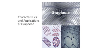
- 2. Graphene is a two-dimensional crystal which composed of tightly- packedcarbon atoms. It is a quasi-two-dimensional material with only one atomic layer thickness, so it is also called monatomic layer graphite. As a new type of nanomaterials with the most thin, the maximum intensity and most conductive conductivity, graphene is known as "black gold" and "king of new materials". On October 5, 2010, professor Andrei Heim and Constantine Novo Shawov from University of Manchester won the 2010 Nobel Prize in Physics for their outstanding achievements in graphene research.
- 3. 1 Characteristics of graphene • Graphene is currently known as the thinnest material. Monolayer graphene has only one carbon atom, and this characteristic of graphene has many features that are not available in graphite. • (1)Strong Conductivity • No mass in Electronics of graphene, so the electrons moving faster than other metal monomer or semiconductor, to a speed that as much as 1/300 of light. That is why the graphene has super conductivity. • (2) Ultra-high hardness • Graphite is the softest mineral, its Mohs hardness is only 1-2, but when it be separated into a carbon atom (graphene), its hardness will higher than diamond which has Mohs hardness of 10 . And graphene has a good tenacity, and can be bend at the same time. • (3) Large specific surface area • Since the thickness of graphene is only one carbon atom, that is 0.335 nm, so graphene has a large surface area. The ideal single-layer graphene specific surface area can reach to 2630 m2 / g and the specific surface area of ordinary activated carbon is 1500 m2 / g. The large specific surface area makes graphene an energy storage material of great potential.
- 4. 2 Application of graphene • (1) A substitute for silicon to produce electronic products • Silicon led us into the digital age, but the researchers are still eager to find some new materials which can make the integrated circuits smaller, faster and cheaper. Graphene has a higher carrier mobility than silicon. Electrons in graphene can run at speed of up to 1/300 of light speed and produce very little heat. The global semiconductor silicon market develop stable, according to IEK's prediction, defect- free single crystals of graphene can replace the crystal silicon in the field of chips, if graphene replace one-tenth of the crystalline silicon made of high-end integrated circuits, the market capacity of graphene is huge.
- 5. (2) A substitute for supercapacitors materials • The supercapacitor is a new type of electrochemical device that stores the energy by polarizing the electrolyte. Emerged from the material science breakthroughIt, the new power-type energy storage components put into mass production a few years ago. Super capacitor has become a new bright spot in the field of chemical power industry. Supercapacitors have great applied value and market potential in field of electric vehicles, hybrid fuel vehicles, special trucks, electricity, railways, communications, defense, consumer electronics and so on. They are widely concerned by all over the world. Because of its high theoretical specific surface area and the independent structure of single-layer graphite crystal, so both sides of the graphene sheet can be negative charge to form an electric double layer. And because of its unique fold and superposition, it can be formed into nano-holes which is conducive to diffusion of electrolyte.
- 6. (3) A substitute for ITO • Currently, the materials in display and touch screen devices are mainly the indium tin oxide(ITO). But indium tin oxide is expensive, bulky, fragile, toxic (comparable to toxicity of lead), while graphene, due to its special molecular structure and high conductivity, is a transparent conductor material. It suitable for the production of display devices. Another feature of graphene is high toughness. As a conductive material in display device, graphene can be folded and stretched. And synthesis of graphene touch screen is environmentally friendly, and with the continuous improvement of production processes, the production costs are expected to significantly lower than the traditional indium tin tin touch screen.
- 7. (4) As additives • Some factories add graphene to cement, paint, paint, plastic, ceramics, photovoltaic glass, cable and other materials to increase the hardness.
- 8. Conclusion • Up till now, Graphene is in the development phase. The graphene produce technology is immature. the main preparation methods are micro-mechanical stripping method (the Nobel Prize winner’s method), epitaxial growth method, oxidative graphite reduction method and gas deposition method. The oxidation method is the main preparation method since the cost is relatively low. There is no company can masss produce graphene , except for some scientific research institutions, the graphene produce of most enterprises are in a small scale of test stage. They has not yet reached the consistency in quality, and finished product is very small, which can not be adapted to industrial applications.