SlideShare a Scribd company logo
1 of 36
Download to read offline
EECT 6378 Power Management Circuits
Chapter 2: Linear Regulators
p g
P f H i L
Prof. Hoi Lee
Department of Electrical Engineering
The University of Texas at Dallas
Voltage Regulators (1)
Voltage regulator is an electronic circuit that provides a
well-specified and stable (regulated) voltage from a less
stable (unregulated) voltage supply for powering different
( g ) g pp y p g
electronic devices.
Major Functions:
Major Functions:
• To provide conversion of a dc input voltage VIN to the desired
dc output voltage within a tolerance range (e.g. VO = 1.2V
1%)
1%).
• To regulate the output voltage VO against variations in the
input voltage VIN, the load current IO (or the load resistance
R ) and the temperature
RL), and the temperature.
• To reduce the output ripple voltage below a specified level.
• To ensure fast response to rapid changes in the input
lt d th l d t ( l d i t )
EE6378 pg. 2
voltage and the load current (or load resistance).
Voltage Regulators (2)
DC voltage transfer function:
O
DC
,
v
V
V
M
where Mv,DC is the voltage conversion ratio
IN
DC
,
v
V
DC current transfer function:
O
I
M
Power efficiency of a dc-dc converter:
IN
O
DC
,
I
I
I
M
DC
,
I
DC
,
v
IN
O
IN
O
in
o M
M
I
I
V
V
P
P
EE6378 pg. 3
IN
IN
in
Voltage Regulators (3)
Static Characteristics:
• Line regulation is the ratio of the output voltage change
V t di h i th i t lt
VO to a corresponding change in the input voltage
)
V
mV
(
|
)
V
V
(
LNR constant
T
and
constant
I
O
A
O
)
V
(
|
)
V
( constant
T
and
constant
I
IN
A
O
EE6378 pg. 4
Voltage Regulators (4)
Static Characteristics:
• Load regulation is the ratio of the output voltage change
V t di h i th l d t
VO to a corresponding change in the load current
)
A
mV
(
|
)
I
V
(
LOR constant
T
and
constant
V
O
A
IN A
IO
A
IN
EE6378 pg. 5
Voltage Regulators (5)
D i Ch i i
Dynamic Characteristics:
Line transient response Load transient response
EE6378 Lecture 2 H. Lee pg. 6
Linear Regulator
Linear regulator is used to describe an dc-dc
regulator in which the voltage or current is
controlled using transistors or other active
devices as variable impedance elements. This
t pe of reg lator is called the linear reg lator
type of regulator is called the linear regulator
because, in the early days, the power device is
realized by transistor (BJT) and normally
operates in the linear region, rather than in the
saturation or cutoff region. If MOS transistor is
g
used as the power device, it will usually operate
in the saturation (pinch-off) region, but the
l t i till k li l t
regulator is still known as a linear regulator
EE6378 pg. 7
R l t b di id d i t t h t l t d
Types of Regulators
Regulators can be divided into two groups: shunt regulators and
series regulators:
A shunt regulator has a variable impedance element in parallel
with the load. The regulator diverts current from the load and thus
control the load voltage
A series regulator has a variable impedance element
connected in series between the unregulated power source
and the load. The voltage across the load is sensed and
impedance of the series element varied so as to keep the load
voltage constant
EE6378 pg. 8
voltage constant
Shunt Regulator
The simplest way of shunt regulator uses the reverse
p y g
breakdown of a Zener diode. The breakdown voltage due
to Zener breakdown mechanism has a negative (-ve)
temperature coefficient while the breakdown voltage due
temperature coefficient, while the breakdown voltage due
to the avalanche multiplication has a positive (+ve)
coefficient. At a breakdown voltage of 5V, both effects are
ti d th t t t ffi i t i l t
active and the net temperature coefficient is close to zero.
Therefore, Zener diode is a good candidate for a voltage
regulator.
g
EE6378 pg. 9
Zener Diode Characteristics
e
I
I V
V
s
z
T
z /
)
1
(
When the zener diode is forward biased, it acts as a normal diode:
C
VT
o
27
at
26mV
voltage
thermal
where
When it is reversed biased, the current follows the diode equation
until the diode undergoes zener breakdown (by tunneling) usually at
a voltage of 6 - 7V
The exact IV characteristic of a zener diode in reverse breakdown
region has a rather complicated mathematical expression. For
simplicity, it is modeled as a battery (Vzk) in series with a resistor (rz):
z
z
zk
z r
I
V
V
EE6378 pg. 10
Zener Diode Regulator (1)
The circuit of a simple zener diode regulator is as:
(2)
)
(
(1)
ZK
Z
Z
s
L
Z
in
ZK
Z
Z
Z
o
V
r
I
R
I
I
V
V
r
I
V
V
We need to express Vo in terms of Vin, VZK and IL by (1) and (2):
( )
)
( ZK
Z
Z
s
L
Z
in
r
R
R
r
L
z
s
z
s
ZK
z
s
s
in
z
s
z
o I
r
R
r
R
V
r
R
R
V
r
R
r
V
EE6378 pg. 11
Zener Diode Regulator (2)
As zener diode current Iz > 0, the load current should be
o
in
L
R
V
V
I
z
s
z
in
o
r
R
V
r
R
r
V
V
Regulation
Line
s
R
For good line and load regulations, both require a small rz which is <<Rs
z
s
z
s
L
o
r
R
r
R
-
I
V
Regulation
Load
The efficiency of the regulator is given as
)
(
power
input
total
power
output
)
(
Efficiency s
L
o
L
o
V
V
V
R
I
V
)
I
(I
V
I
V
The efficiency is the largest when the load current is maximum and the
source voltage is minimum
)
(
power
input
total o
in
in
z
L
in V
V
V
)
I
(I
V
EE6378 pg. 12
source voltage is minimum
Example
Two-stage shunt regulator:
Find the line and load regulations of above circuit where V =26V
Find the line and load regulations of above circuit where Vin=26V.
What are advantages of using the two-stage shunt regulator compared
to the simple shunt regulator (without Rs2 and the second zener diode)?
EE6378 pg. 13
Answers
2 t d i li l ti 2 77 V/V d
2-stage design: line regulation = 2.77mV/V and
load regulation = -9.7V/A
1 stage design: line regulation = 90 9mV/V and
1-stage design: line regulation = 90.9mV/V and
load regulation = -18.2V/A
Two stage design improves both line and load
Two-stage design improves both line and load
regulations of the shunt regulation
EE6378 pg. 14
Series Regulator
Series regulators have a variable impedance element between the
source and the load. As the load current or source voltage varies, the
impedance of the series element is adjusted to keep the output voltage
constant. Therefore, the only current in the series element is the load
current and its efficiency is given by
circuitry
control
the
in
current
supply
the
is
I
re
whe
)
(
q
in
o
q
o
in
o
o
V
V
I
I
V
I
V
The efficiency does not depend on the load current, only on the ratio of
load-to-source voltage. Series regulator is thus generally preferred
load to source voltage. Series regulator is thus generally preferred
compared to the shunt regulator.
EE6378 pg. 15
Basic Concept (1)
Using voltage-divider model,
value of output voltage Vo
p g o
in
p
L
L
o V
R
R
R
V
Vo can be maintained constant
by changing the value of RP
h R V b th h
Voltage Divider Model
when RL, Vin or both change
Negative feedback control
circuitry measures V and
circuitry measures Vo and
controls the value of Rp to
achieve the desired Vo
Linear Regulator Model
EE6378 pg. 16
Basic Concept (2)
Power efficiency of the linear regulator
L
d
i
L I
V
V
I
V
cont
L
L
in
do
in
in
L
in
o
V
I
I
I
)
V
V
V
(
I
I
V
V
where V is the dropout voltage (V V ) and I is
in
do
V
V
1
where Vdo is the dropout voltage (Vin - Vo) and Icont is
the current consumption of the controller. Normally,
Icont << IL
Icont IL
To maximize , Vdo should be minimized (i.e. Rp
should be much smaller than RL)
EE6378 pg. 17
L)
Structure of Series Regulator
Vin
Below is a typical series regulator which consists of four main building
blocks:
Vref
Q1
Va
A(s)
V
Vo
Rf2 r
V-
Vfb
R
RL
rc
C
Rf1 C
EE6378 pg. 18
Structure of Series Regulator (2)
Voltage Reference (Vref): a very stable voltage with
respect to temperature change and input voltage
variations usually of the bandgap type
variations, usually of the bandgap type.
Error Amplifier (A(s)): a very high (dc) gain opamp to
achieve a close to zero error signal Verr=V+-V-.
Feedback Network: Rf1 and Rf2 define the feedback
factor and generate Vfb to be compared with Vref to get
the designed output voltage V
the designed output voltage Vo.
Series Pass/Power Transistor (Q1): power transistor
configuration to pass high current from the source to
output. As it handles large current, the size of pass
transistor dominates the area of the whole series
regulator.
EE6378 pg. 19
regulator.
Questions
If Vref = 1.2V, Rf1 = 1M ,
Rf2 = 3M , what is the
value of Vo?
If VCE,sat,Q1 = 0.2V, what
is the minimum input
supply voltage of the
linear regulator?
linear regulator?
If the offset voltage Voff
of the error amplifier is
20mV what is the
20mV, what is the
percentage change in
the output voltage?
Repeat this if input stage V
ML
M3 M4
V1
Repeat this if input stage
of the error amplifier is
PMOS transistors and
Vref = 0.5V.
Vo
Mb1
Mb2
Mb3
M1 M2
Cm
Vin
EE6378 pg. 20
ref
Answers
Vo = Vref(1+Rf2/Rf1) = 1.2(1+3) = 4.8V by assuming dc gain of the error
amplifier is very large.
Vin,min = max(Vo+VBE,Q1+Vov,ML, Vo+VCE,sat,Q1) = Vo+VBE,Q1+Vov,ML =
4.8+0.7+0.15=5.65V.
Vo’= (Vref+Voff)(1+Rf2/Rf1) = (1.22)(1+3) = 4.88V that corresponds to
1.67% increase in the output voltage. Therefore, it is very important to
i i i th ff t f th lifi i d t i th f
minimize the offset of the amplifier in order to improve the accuracy of
the linear regulator.
If Vref = 0.5V, then Vo = 2V and Vin,min = 2+0.7+0.15 = 2.85V. With 20mV
offset of the error amplifier, Vo’ = 2.08V that corresponds to 4% increase
in the output voltage. Therefore, the output voltage variation of the
l t i h ll l f lt i d
EE6378 pg. 21
regulator increases when a small-value reference voltage is used.
Concerns of Series Regulator
The linear regulator can only perform step down dc-dc
The linear regulator can only perform step down dc dc
conversion. i.e. Vo < Vin
Since = Vo/Vin, with Vo = 5V and Vin = 10V, = 50%.
Therefore, linear regulator has a very poor efficiency if
the difference between Vo and Vin is large. The wasted
power is mainly dissipated by the power transistor Q1 as
heat.
EE6378 pg. 22
Concern of Using NPN Pass Transistor
With a Li-Ion battery as Vin, Vin varies from 2.7V to 4.2V.
The maximum output voltage of the linear regulator
using NPN pass transistor is Vin,min-VBE,Q1-Vov,ML 2.7-
0.7-0.15 = 1.85.
Efficiencies of linear regulator with V = 1 85V:
Efficiencies of linear regulator with Vo = 1.85V:
• max = Vo/Vin,min = 1.85/2.7 = 68.5%.
• min = Vo/Vin max = 1.85/4.2 = 44%.
min Vo/Vin,max 1.85/4.2 44%.
Efficiency of the linear regulator using NPN transistor is
very poor!
Poor efficiency will also be resulted from using NMOS
transistor as the pass transistor.
EE6378 pg. 23
The linear regulator uses negative feedback loop to keep the output voltage constant with
Principle of Operation (1)
The linear regulator uses negative feedback loop to keep the output voltage constant with
respect to the change of input supply and load current.
Negative feedback loop consists of feedback resistors (Rf1 & Rf2), error amplifier and Q1
For example: when Io
o
Vo as load current is initially drawn from the output capacitor
Vfb as Vfb = (Rf1/(Rf1+Rf2))Vo
Va = A(Vref-Vfb)
V (N i f db k V i i i i i l l )
Negative
Feedback
Vo (Negative feedback causes Vo to maintain its original value)
Same reasoning explains why Vo can maintain a relatively constant value when IL
decreases.
EE6378 pg. 24
Principle of Operation (2)
When Vin
Vo as collector current of Q1 increases
Vfb as Vfb = (Rf1/(Rf1+Rf2))Vo
V = A(V V )
Negative
Va = A(Vref-Vfb)
Vo (Negative feedback causes Vo to maintain its original value)
Same reasoning explains why Vo can maintain a relatively constant value when Vin
decreases.
Feedback
Vo
ML
M3 M4
C
V1
EE6378 pg. 25
Mb1
Mb2
Mb3
M1 M2
Cm
Vin
Review on Feedback Theory
Typical Feedback System
Define: A – Open-loop gain
b – Feedback factor
L = Ab loop gain
L = Ab – loop gain
Af – Closed-loop gain
1+Ab – amount of feedback
1
Ab
if
1
1
)
(
b
Ab
A
x
x
A
Abx
Ax
x
x
A
Ax
x
i
o
f
o
i
f
i
e
o
EE6378 pg. 26
Linear Regulator as Feedback System (1)
o
o
in
a
o R
I
V
V
V
where Ro is the equivalent resistance at output
o
o
in
o
ref
o
o
in
fb
ref
o
o
in
a
o
R
I
V
bV
V
A
R
I
V
V
V
A
)
(
)
(
o
o
in
ref
o I
Ab
R
V
Ab
V
Ab
A
V
1
1
1
1
EE6378 pg. 27
Linear Regulator as Feedback System (2)
o
o
in
ref
o I
Ab
R
V
Ab
V
Ab
A
V
1
1
1
1
on
Based
A
V 1
b
Ab
A
V
V
ref
o 1
1
Larger b can improve the accuracy of the output voltage
with respect to the variation of the reference voltage
Ab
Ab
V
V
in
o 1
1
1
with respect to the variation of the reference voltage.
R
V o
o
Line regulation is improved by the loop gain of feedback system.
Larger dc loop-gain magnitude gives better line regulation.
Ab
Io 1
Load regulation is improved by the loop gain of feedback system.
Larger dc loop-gain magnitude gives better load regulation.
EE6378 pg. 28
Loop-Gain Analysis (1)
Break the loop and analyze the loop gain L(s) of linear
regulator for stability.
)
(
)
(
)
(
s
V
s
V
s
L fb
EE6378 pg. 29
Loop-Gain Analysis (2)
Two assumptions:
• Error amplifier has zero output resistance: va = -A(s)v-
• Rf1, Rf2 >> R such that (Rf1+Rf2)//R R
v
v
v
v
v
v
v
v
s
L a
a
o
o
fb
fb
)
(
f1, f2 ( f1 f2)
a
L
c
L
o v
SC
r
R
r
SC
r
R
v
)]
/
1
//(
)[
1
(
)]
/
1
//(
)[
1
(
v
v
v
v a
o
c
L SC
r
R
r )]
/
1
//(
)[
1
(
)
1
(
)
(
1
)
1
(
)
1
(
L
L
c
L
o
r
R
r
R
r
sCr
R
r
R
v
v
]
)
1
(
)
1
(
)
(
[
1
)
1
(
L
c
L
c
L
L
a
R
r
r
R
r
R
r
sC
R
r
v
EE6378 pg. 30
Loop-Gain Analysis (3)
]
)
1
(
)
1
(
)
(
[
1
1
)
1
(
)
1
(
L
c
L
c
L
c
L
L
a
o
R
r
r
R
r
R
r
sC
sCr
R
r
R
v
v
LHP zero z: 1/Crc; LHP Pole p: ]
)
1
(
)
1
(
)
(
[
/
1
L
c
L
c
L
R
r
r
R
r
R
r
C
• Since ESR of a large capacitor is usually very small such that rc can
usually be neglected when compared to RL. For example: the ESR
of a 10 F capacitor is as small as 50m .
• The emitter resistance of the pass transistor is much smaller than
the load resistance. For example: 1/gm << RL or r << (1+ )RL
1
)
1
(
)
1
(
)
( L
L
L
L r
r
R
R
r
r
R
r
R
r
)
/
1
(
1
and
1
1
1
)
1
(
)
1
(
)
1
(
)
1
(
)
(
p
m
c
c
z
c
m
c
L
c
L
L
L
c
L
c
L
g
r
C
Cr
r
g
r
r
R
r
R
R
r
R
r
r
R
r
R
r
EE6378 pg. 31
)
/
1
( m
c
c g
r
C
Cr
Loop-Gain Analysis (4)
z
f
o
f
fb
s
v
s
A
R
R
R
v
R
R
R
v
/
1
/
1
]
)
(
[
1
1
z
f
fb
p
f
f
o
f
f
fb
s
R
s
A
v
s
L
s
R
R
R
R
/
1
)
(
)
(
Therefore,
/
1
1
2
1
2
1
p
f
f s
R
R
s
A
v
s
L
/
1
)
(
)
(
Therefore,
2
1
)
/
1
(
1
and
1
where p
z
g
r
C
Cr )
/
1
( m
c
c g
r
C
Cr
The pole is located at lower frequency than that of zero.
EE6378 pg. 32
Loop-Gain Analysis (5)
A( ) i th t f f ti f t d lifi
A(s) is the transfer function of an uncompensated amplifier
with a dominant pole 1 and a very high-frequency pole 2.
Loop gain is always stable if z is located close to 1.
EE6378 pg. 33
Loop gain is always stable if z is located close to 1.
Concerns of Loop-Gain Compensation
As mentioned before, z should be close to 1 for
stability. There are concerns to allow z located at low
frequency:
frequency:
• We can increase CL to push z to a lower frequency. However,
the first pole of loop-gain function p also decreases. The unity-
i b d idth f th l i f ti d d h
gain bandwidth of the loop-gain function decreases and hence
load transient response of linear regulator degrades.
• We can increase rc to push z to a lower frequency by using a
physical resistor in addition to the ESR of C However large r
physical resistor in addition to the ESR of CL. However, large rc
also significantly degrades the load transient response of the
linear regulator.
In practical situations, it is difficult to realize low-
frequency z without suffering from the tradeoff.
EE6378 pg. 34
frequency z without suffering from the tradeoff.
Why Low-Dropout Regulator ? (1)
With a Li-Ion battery as Vin, Vin
varies from 2.7V to 4.2V. The
maximum output voltage of the Vin
p g
linear regulator using NPN pass
transistor is Vo,max= Vin,min-VBE,Q1-
Vov,ML 2.7-0.7-0.15 = 1.85 in order
Vref
Vo
Q1
Va
A(s)
V-
to allow the linear regulator to
function properly
Dropout Voltage (Vdo) is the
o
Vfb
Rf2
RL
rc
minimum voltage difference
between the input and output
under which the regulator still
able to maintain the o tp t ithin
Rf1
RL
C
able to maintain the output within
the specification
In this case, Vdo,max = 4.2-1.85 =
2 35V
EE6378 pg. 35
2.35V
Why Low-Dropout Voltage ? (2)
As mentioned before, efficiencies of linear regulator with
V =1 85V can be as low as
Vo=1.85V can be as low as
• min = Vo/Vin,max = Vo/(Vo+Vdo,max) = 1.85/(1.85+2.35) =
44%
For portable equipment, a 2.35V dropout voltage is not
efficient. To solve this problem, a low-dropout voltage
p , p g
regulator (LDO or LDR) is designed to allow the input
voltage to go down to a very low value above Vo by
changing the pass transistor from NPN/NMOS
transistor to PNP/PMOS transistor.
EE6378 pg. 36
Choice of Power Transistor (1)
Using nMOS as Rp
• Smaller power device size
to handle the same load
Using pMOS as Rp
Good power efficiency as Vdo
is independent of V (Low
to handle the same load
current
• Poor power efficiency due
f
is independent of Vg (Low-
dropout regulator)
Low frequency pole at node
V d d th t bilit
EE6378 pg. 37
to large Vdo if Vg Vin Vg degrades the stability
Choice of Power Transistor (2)
Different Vg maintains the
fixed Vo by varying Vdo under
different V and fixed I
Different Vg maintains the
fixed Vo under different It
(both V and V are fixed)
Power device Mp can operate either in the triode region
or saturation region!
different Vin and fixed It (both Vin and Vdo are fixed)
W
1
1
W
)
V
1
(
)
V
V
V
(
L
W
C
2
1
I do
2
th
o
g
ox
t
EE6378 pg. 38
)
V
2
1
V
)
V
V
V
(
L
W
C
I 2
do
do
th
o
g
ox
t
Structure of LDO
Design Issues:
• Power PMOS transistor
• Error Amplifier
• Rf1 and Rf2 made of the same material
• Voltage Reference
• Stability and speed of feedback loop
EE6378 pg. 39
y
• Choice of output off-chip capacitor
Specifications of LDO
Two Categories:
• Regulating (accuracy) performance
Line regulation, load regulation, temperature dependence,
transient overshoot, transient recovery time, stability
• Power Characteristics
Io, Quiescent current Iq, Vin & Vo ( & I)
EE6378 pg. 40
Efficiency (1)
C t Effi i
Current Efficiency I:
I = Io/(Io+Iq) where Iq is the quiescent current of LDO
Iq=I1+I2+I3
In LDO design for portable applications I is usually much larger than I with
In LDO design for portable applications, Io is usually much larger than Iq with
> 99% efficiency
When Io is 0, Iq should be minimized (I3 should be small by using large values
of Rf1 and Rf2)
EE6378 pg. 41
Efficiency (2)
1 do
o
o
o
o V
V
I
V
P
-
1
)
( 3
2
1 in
do
in
o
o
in
o
o
in
o
V
V
V
V
I
I
I
I
V
I
V
P
P
Smaller dropout voltage causes a higher power conversion efficiency
especially Io >> Iq
In light-load condition (small Io), the efficiency is poorer as I1, I2, and
I3 are close to Io
EE6378 pg. 42
Dropout Voltage and Power-Transistor Sizing
)
/
(
2
where
L
W
C
I
V o
ov
)
/
( L
W
Cox
p
VSD is larger than Vov to allow LDO operating in the
SD ov
saturation region
Design at the worst case: largest Vov at Io(max) and
p(min) at the maximum temperature
(
By using minimum L (the smallest transistor and
hence parasitic capacitance), keep increasing W
until meeting the dropout specification
IR at the routing metals increase V
IR at the routing metals increase VDO
Design margin by experience-generally the chosen
W is 1.1-1.2 times of the theoretical W
EE6378 pg. 43
Load Regulation
Vref
A(s) L
R
I
V
R o
L
o
1
Vin
RL
rc
Rf2
Vfb
Vo
L
C
Rf1
Load Regulation (R): closed-loop output resistance of LDO
Ro is the open-loop output resistance of the pass transistor as
Rf1, Rf2 >> Ro
Rf1, Rf2 Ro
Better load regulation is achieved by smaller Ro (using minimum
channel length of the pass transistor) and larger loop-gain
magnitude
EE6378 pg. 44
As Ro 1/Io, high Io range gives better load regulation
Line Regulation
I
Vref
A(s)
V
L
R
I
V
R o
L
o
1
in
o
mp
V
I
g
Vin+ Vin
RL
rc
Rf2
Vfb
Vo
A
R
g
R
V PT
o
mp
o 1
C
Rf1
b
A
b
A
A
A
L
g
R
g
V
V
PT
PT
o
mp
mp
in
o 1
1
1
gmp is the transconductance of power PMOS transistor
Line regulation is independent of the gain of the power transistor
Line regulation can be improved by a high-gain error amplifier
Other error sources on line regulation are voltage reference and
ff t lt f th lifi
EE6378 pg. 45
offset voltage of the error amplifier
Review on Voltage Gain
Vin
Transconductance Cell
(Gm)
Vo
Io
Ro
i
o
m
v
i
G
in
o
o
o
m
in
o
v
R
i
R
G
v
v
Gain Stage
in
v in
in v
v
Gm and Ro can be found individually
Input-Output voltage gain can be found by the product of Gm and
p p g g y p m
Ro
EE6378 pg. 46
Line Regulation Including Other Errors
o
I
Vref
A(s)
V
L
R
I
V
R o
L
o
1
in
o
mp
V
I
g
Vin+ Vin
Vref
Vos
RL
rc
Rf2
Vfb
Vo
1 V
V
R
V
C
Rf1
)
)(
1
(
1
1
2
in
os
in
ref
f
f
in
o
V
V
V
V
R
R
b
A
V
V
LDO feedback loop Error amp. and Vref
Voltage gain of the error amplifier is not the only parameter to
improve line regulation
Good designs on supply independence of Vref and reducing
EE6378 pg. 47
g pp y p ref g
systematic offset of error amplifier are very important
Temperature Coefficient
I
Vref
A(s)
L
R
I
V
R o
L
o
1
in
o
mp
V
I
g
Vref
Vos
Vin
RL
rc
Rf2
Vfb
Vo
os
L
C
Rf1
)
)(
1
(
1
2
T
V
T
V
R
R
T
V os
ref
f
f
o
V i ti f V t diff t t t d d b th lt
Variation of Vo at different temperature depends on both voltage
reference and error amplifier design
Rf1 and Rf2 must be made by the same material and closely
placed
EE6378 pg. 48
placed
Load Transient Response (1)
Note that:
• Re = rc (previous notes)
• Co = C (previous notes)
EE6378 pg. 49
Load Transient Response (2)
Better load transient response by tresp , Co , Re and Lc .
EE6378 pg. 50
AC Design (1): Loop-Gain Analysis
)
R
R
R
(
)
C
sR
1
(
z
R
g
g
|
V
V
|
L
2
1
1
pa
a
o
a
mp
ma
n
fb
o
L(s) = Vfb/Vn = loop gain of the LDO
Lo = |Vfb/Vn| = loop-gain magnitude
(Vfb/Vn) = phase of loop gain that starts at 180o
t t i d t V
EE6378 pg. 51
zo = output impedance at Vo
AC Design (2): Loop-Gain Analysis
o
o
e
x
o
sC
C
sR
r
z
1
// L
o
x R
R
R
r
r //
)
//( 2
1
L
o R
R
R
r )
( 2
1
In no-load condition, IL=0
Note:
)
( 2
1 R
R
R
r L
o
In heavy-load condition, IL>>0 ro is the output
resistance of power
transistor Mp
o
x r
r
In both conditions
o
x
o
o
e
o
o
o
C
sr
R
sC
r
z
1
)
1
(
EE6378 pg. 52
AC Design (3): Loop-Gain Analysis
)
R
R
R
(
)
C
sr
1
)(
C
sR
1
(
)
C
sR
1
(
r
r
g
g
|
V
V
|
L
2
1
1
o
o
pa
a
o
e
o
a
mp
ma
n
fb
o
The system has 2 poles and 1 zero
o
oC
r
p
1
1
1
pa
a
2
C
R
1
p
1
o
e
e
C
R
z
1
EE6378 pg. 53
AC Design (4): Loop-Gain Analysis
ze should cancel p2 within one decade of
frequency for stability
Parasitic pole(s), ppar, must be far away
p
from the unity-gain frequency (UGF)
Different UGFs are resulted from
different Re values such as ze locating
before or after p2
p2 locates at very low frequency as Cpa
and Ra are large
Required large Co and Re
• Large Co decreases the unity-gain
frequency
• Large Re degrades load transient
response
• Low-frequency pole-zero cancellation is
f bl t l d t i t
EE6378 pg. 54
unfavorable to load transient recovery
time
LDO with Voltage Buffer
Smaller required Re can be achieved by inserting a low output-
resistance (1/gmb) voltage buffer
( gmb) g
One more pole (p3) is created but is located at high frequency due to
small output resistance of the voltage buffer
p2 (with voltage buffer) locates at a higher frequency than the one
EE6378 pg. 55
p2 (with voltage buffer) locates at a higher frequency than the one
without voltage buffer (Cb << Cg)
Effect of Load Currents on Stability
L i i ll h I
Loop gain is smaller when Io
becomes larger due to gmpro
1/ Io
p1 is moved to a higher frequency
at a faster rate than the decrease
in loop gain magnit de hen I
in loop-gain magnitude when Io
increases due to smaller ro of the
power transistor (ro 1/Io)
Hence, Distance between p1 and
p2 becomes smaller when Io
increases and the worst case
increases and the worst-case
stability occurs at maximum Io
C
EE6378 pg. 56
Compensation is needed at max.
Io
Effect of Loop-Gain Magnitude on Stability
Larger loop gain by increasing Ra of
the error amplifier
p2 p2’
A l R i d d t t
A larger Re is needed to create a zero
at lower frequency (ze ze’)
Larger loop gain more unstable as
p3 may be below the UGF of loop
gain
A larger Co is generally needed
EE6378 pg. 57
Loop Gain Simulation
L(j )=Vfb(j )/Vn(j )
Information lower than 1/( LxCx) is not valid
EE6378 pg. 58
Summary of LDO Specifications
Specifications Approaches for Improvement
Stability Lo and UGF
Output voltage error due to finite
loop gain
Lo
Line regulation Lo
g o
Load regulation Lo
T i t
UGF , PM , SR , Co and
Transient response
, , , o
ESR
Where
L = loop gain magnitude UGF = unity gain frequency of the loop gain response
Lo = loop-gain magnitude, UGF = unity-gain frequency of the loop-gain response,
PM = phase margin of the loop-gain response, SR = slew rate at the gate of the
power transistor, Co = off-chip output capacitor, ESR = equivalent series resistance
of the off-chip output capacitor
EE6378 pg. 59
Circuit Implementations (1)
Mb2
Mp
Mb2
Me1
Circuit of LDO consists of
• R1 and R2
• Cin and Co
• V f
Vref
• Error Amplifier
• Voltage Buffer
• Power Transistor
V V V V
EE6378 pg. 60
Vin,min = Vov,Me1 + Vgs,Mb2 + Vgs,Mp
Circuit Implementations (2)
BJT has a small VBE drop (~0.7V)
The circuit can operate at lower input supply compared to the
previous case
previous case
Smaller input capacitance for small VBE
Base current introduces larger offset voltage and hence degrades
f h l
EE6378 pg. 61
accuracy of the output voltage
Circuit Implementations (3)
Vthn << |Vthp| is needed to turn off the power PMOS transistor
effectively when Io=0
Some circuit uses npn BJT transistor instead, but non-zero current is
a problem and npn BJT transistor is not available in standard n-well
CMOS technologies
EE6378 pg. 62
Circuit Implementations (4)
Better matching by BJT
Non-zero base current, but micro-ampere collector current with a
large current gain
large current gain
Better input common-mode range
NPN BJT transistor is unavailable in standard n-well CMOS
technologies
EE6378 pg. 63
technologies
Review on Device Matching
Matching of Using NPN Input Pair
)
)
/
(
)
/
(
(
)
(
)
(
, p
T
mp
thp
npn
s
T
os
L
W
L
W
V
g
g
V
I
I
V
V
Matching of Using NMOS Input Pair
)
/
(
,
, p
BJT
m
p
npn
s L
W
g
I
)
)
/
(
)
/
(
)
/
(
)
/
(
(
2
)
(
)
(
,
p
p
n
n
thn
n
gs
mn
mp
thp
thn
os
L
W
L
W
L
W
L
W
V
V
g
g
V
V
V
VT = thermal voltage of BJT transistor 26mV,
gm,BJT >> gmn under the same bias current
V (V V ) h (V V ) 150 V
VT << (Vgs,n – Vthn) where (Vgs,n – Vthn) 150mV
mV
V
mV
I
I
V thn
npn
s
npn
s
T 10
4
)
(
,
,
EE6378 pg. 64
Circuit Implementations (5)
Limited output swing causes limited Vgs of the power PMOST
A large transistor size is therefore required
Few pairs of device to match lower random offset voltage
EE6378 pg. 65
Few pairs of device to match lower random offset voltage
Pros & Cons of Linear Regulators
Advantages:
• Simple structure which can be fabricated on a single chip
• Very few external components needed May need as few as only
• Very few external components needed. May need as few as only
the input and output filtering capacitors
• For system design, very easy to use. The IC may have only 3
pins V V and GND
pins, Vin, Vo and GND
• Small output ripple, good line and load regulations
• Apparently no electromagnetic interference (EMI) problem
Disadvantages:
• Very low efficiency which is limited to V /V if V is large
• Very low efficiency which is limited to Vo/Vin if Vdo is large
• May need bulky heat sink to dissipate waste heat
• Vo has to be lower than Vin. i.e. step down only
EE6378 pg. 66
Protection Circuitries
It is important when designing linear regulators is
protection against undesirable factors that are inherent
p g
to the working environment of the application.
As the power pass device dissipates most power,
protection usually revolves around its operating
conditions. Operating limits are defined by power
dissipation, output current range, breakdown voltage,
temperature ratings, etc.
Overload protection (current limiting) and thermal
shutdown are two most common methods to protect
power pass transistor.
EE6378 pg. 67
Structure of Linear Regulator with Protection
Structure of linear regulator adopting both over
Structure of linear regulator adopting both over-
current protection and thermal shutdown:
EE6378 pg. 68
Overload Protection
A frequent occurrence of overload is to short the output
node Vo to ground. For example, if specifications limit the
maximum output current 200mA the minimum load
maximum output current 200mA, the minimum load
resistor is 10 for Vo = 2V. It is understandable that an
user of the linear regulator accidentally placing a 5 at
th t t f th li l t l d
the output of the linear regulator can cause overload
condition. Therefore overload protection is important.
The most effective way to prevent overload is to steal the
base current of the power transistor.
• The protection consists of Rsc and Q3. Rsc is a low resistance
high power resistor (e g 0 1 with power rating of 10W)
high power resistor (e.g. 0.1 with power rating of 10W)
• When Io , VRsc . When VRsc=VBE3(on)=0.7V, Q3 turns on and
steals IB from the power transistor
I i li it d t I V /R
EE6378 pg. 69
• Io is limited to Isc = VBE3(on)/Rsc
Thermal Shutdown (1)
When large current passes though the power transistor
Q1 excess heat will raise the junction temperature T of
Q1, excess heat will raise the junction temperature Tj of
Q1. When Tj = 150 C (or 175 C), Q1 breaks down and
will be damaged permanently.
The thermal shutdown circuit consists of R7, R8 and Q4.
R and R form a voltage divider with V = 0 4V
R7 and R8 form a voltage divider with VBE4 = 0.4V.
Therefore, Q4 is OFF at room temperature. Therefore,
R7, R8 and Q4 will not affect the circuit operation at room
temperature.
EE6378 pg. 70
Thermal Shutdown (2)
Assume VBE4(on)(25 C) = 700mV and the tempco of VBE
is around -2mV/ C.
At 175 C, VBE4(on)(175 C) = 700mV-(2mV)(175-25) =
400mV. Further increase in temperature above 175 C
p
will turn on Q4 hard, stealing base current from the pass
transistor. As a result, the load current decreases and
heat generated from Q1 will decrease.
g
Q4 should have excellent thermal coupling with Q1. In
addition V is a bandgap reference and the reference
addition, Vref is a bandgap reference and the reference
voltage will become more or less constant over wide
range of temperature.
EE6378 pg. 71
Some Related References
G. A. Rincon-Mora, et. al., “A low-voltage, low quiescent current, low
dropout regulator,” IEEE JSSC, pp. 36-44, Jan. 1998.
p g pp
G. A. Rincon-Mora, et. al., “Active capacitor multiplier in Miller-
Compensated Circuits,” IEEE JSSC, pp. 26-32, Jan. 2000.
K. N. Leung, et. al., “A capacitor-free CMOS low-dropout regulator
K. N. Leung, et. al., A capacitor free CMOS low dropout regulator
with damping-factor-control frequency compensation,” IEEE JSSC,
pp. 1691-1702, Oct. 2003.
P. Hazucha et. al., “Area-efficient linear regulator with ultra-fast load
P. Hazucha et. al., Area efficient linear regulator with ultra fast load
regulation,” IEEE JSSC, pp. 933-940, Apr. 2005.
M. Al-Shyoukh et. al., “A transient-enhanced low-quiescent current
low-dropout regulator with buffer impedance attenuation,” IEEE
low dropout regulator with buffer impedance attenuation, IEEE
JSSC, pp. 1732-1742, Aug. 2007.
EE6378 pg. 72

More Related Content

What's hot

Unit-2 AC-DC converter
Unit-2 AC-DC converter Unit-2 AC-DC converter
Unit-2 AC-DC converter johny renoald
 
tca785
tca785tca785
tca785101conan
 
Cycloconverters
CycloconvertersCycloconverters
CycloconvertersVishal_popat
 
Relaxation oscillators
Relaxation oscillatorsRelaxation oscillators
Relaxation oscillatorsTouqeer Jumani
 
Calculating the efficiency and regulation of transformer using matlab
Calculating the efficiency and regulation of transformer using matlabCalculating the efficiency and regulation of transformer using matlab
Calculating the efficiency and regulation of transformer using matlabMafaz Ahmed
 
Oscillators
OscillatorsOscillators
Oscillators12nitin
 
Three Phase Controlled Rectifier Study in Terms of firing angle variations
Three Phase Controlled Rectifier Study in Terms of firing angle variationsThree Phase Controlled Rectifier Study in Terms of firing angle variations
Three Phase Controlled Rectifier Study in Terms of firing angle variationsIDES Editor
 
Unit- 4 inverters (part-2)
Unit- 4 inverters (part-2)Unit- 4 inverters (part-2)
Unit- 4 inverters (part-2)johny renoald
 
2 transistor thyristor
2 transistor thyristor2 transistor thyristor
2 transistor thyristorRaghu Selvaraj
 
Transient response of RC , RL circuits with step input
Transient response of RC , RL circuits  with step inputTransient response of RC , RL circuits  with step input
Transient response of RC , RL circuits with step inputDr.YNM
 
1 ph semi converter (r-l load)
1 ph semi converter (r-l load)1 ph semi converter (r-l load)
1 ph semi converter (r-l load)avi1001
 
FREQUENCY ENTRAINMENT IN A WIEN BRIDGE OSCILLATOR
FREQUENCY ENTRAINMENT IN A WIEN BRIDGE OSCILLATORFREQUENCY ENTRAINMENT IN A WIEN BRIDGE OSCILLATOR
FREQUENCY ENTRAINMENT IN A WIEN BRIDGE OSCILLATOR SwgwmsaBoro
 
Power Electronics - Thyristor Commutation
Power Electronics - Thyristor CommutationPower Electronics - Thyristor Commutation
Power Electronics - Thyristor CommutationBurdwan University
 
Unit 4 inverters (part-1)
Unit 4 inverters (part-1)Unit 4 inverters (part-1)
Unit 4 inverters (part-1)johny renoald
 
Power electronics question bank
Power electronics question bankPower electronics question bank
Power electronics question bankmcpriya04
 
Controlled Rectifier
Controlled RectifierControlled Rectifier
Controlled RectifierFaraz Ahmed
 

What's hot (20)

Unit-2 AC-DC converter
Unit-2 AC-DC converter Unit-2 AC-DC converter
Unit-2 AC-DC converter
 
Unit 3
Unit 3Unit 3
Unit 3
 
tca785
tca785tca785
tca785
 
Cycloconverters
CycloconvertersCycloconverters
Cycloconverters
 
Relaxation oscillators
Relaxation oscillatorsRelaxation oscillators
Relaxation oscillators
 
Calculating the efficiency and regulation of transformer using matlab
Calculating the efficiency and regulation of transformer using matlabCalculating the efficiency and regulation of transformer using matlab
Calculating the efficiency and regulation of transformer using matlab
 
Oscillators
OscillatorsOscillators
Oscillators
 
Three Phase Controlled Rectifier Study in Terms of firing angle variations
Three Phase Controlled Rectifier Study in Terms of firing angle variationsThree Phase Controlled Rectifier Study in Terms of firing angle variations
Three Phase Controlled Rectifier Study in Terms of firing angle variations
 
Unit- 4 inverters (part-2)
Unit- 4 inverters (part-2)Unit- 4 inverters (part-2)
Unit- 4 inverters (part-2)
 
2 transistor thyristor
2 transistor thyristor2 transistor thyristor
2 transistor thyristor
 
Transient response of RC , RL circuits with step input
Transient response of RC , RL circuits  with step inputTransient response of RC , RL circuits  with step input
Transient response of RC , RL circuits with step input
 
1 ph semi converter (r-l load)
1 ph semi converter (r-l load)1 ph semi converter (r-l load)
1 ph semi converter (r-l load)
 
FREQUENCY ENTRAINMENT IN A WIEN BRIDGE OSCILLATOR
FREQUENCY ENTRAINMENT IN A WIEN BRIDGE OSCILLATORFREQUENCY ENTRAINMENT IN A WIEN BRIDGE OSCILLATOR
FREQUENCY ENTRAINMENT IN A WIEN BRIDGE OSCILLATOR
 
Power Electronics - Thyristor Commutation
Power Electronics - Thyristor CommutationPower Electronics - Thyristor Commutation
Power Electronics - Thyristor Commutation
 
Unit 4 inverters (part-1)
Unit 4 inverters (part-1)Unit 4 inverters (part-1)
Unit 4 inverters (part-1)
 
DC DC Converter
DC DC ConverterDC DC Converter
DC DC Converter
 
Power electronics question bank
Power electronics question bankPower electronics question bank
Power electronics question bank
 
Controlled Rectifier
Controlled RectifierControlled Rectifier
Controlled Rectifier
 
Dual converter
Dual converterDual converter
Dual converter
 
Pdc manual
Pdc manualPdc manual
Pdc manual
 

Similar to Ee6378 linear regulators

Exp2 voltage regulator
Exp2 voltage regulatorExp2 voltage regulator
Exp2 voltage regulatorModugu Srinivas
 
Lecture note macine & drives (power electronic converter)
Lecture note macine & drives (power electronic converter)Lecture note macine & drives (power electronic converter)
Lecture note macine & drives (power electronic converter)Faiz Mansur
 
Voltageregulator 131207222403-phpapp02
Voltageregulator 131207222403-phpapp02Voltageregulator 131207222403-phpapp02
Voltageregulator 131207222403-phpapp02Sridhar Done
 
Ee 791 drives lab maual
Ee 791 drives lab maualEe 791 drives lab maual
Ee 791 drives lab maualDivya15121983
 
Ch_5 Regulated Power Supply.pdf
Ch_5 Regulated Power Supply.pdfCh_5 Regulated Power Supply.pdf
Ch_5 Regulated Power Supply.pdfDhwajshah2
 
Voltage Regulators IC
Voltage Regulators ICVoltage Regulators IC
Voltage Regulators ICDr.Raja R
 
CVT design
CVT designCVT design
CVT designbinodsahu8
 
Chapter 5 - DC-AC Conversion.pdf
Chapter 5 - DC-AC Conversion.pdfChapter 5 - DC-AC Conversion.pdf
Chapter 5 - DC-AC Conversion.pdfbenson215
 
377275109-Ch-2-Uncontrolled-Rectifiers-Autosaved.pptx
377275109-Ch-2-Uncontrolled-Rectifiers-Autosaved.pptx377275109-Ch-2-Uncontrolled-Rectifiers-Autosaved.pptx
377275109-Ch-2-Uncontrolled-Rectifiers-Autosaved.pptxpriyakunduq
 
Chapter 1 - PWM DC-DC Converter.pdf
Chapter 1 - PWM DC-DC Converter.pdfChapter 1 - PWM DC-DC Converter.pdf
Chapter 1 - PWM DC-DC Converter.pdfbenson215
 
Analog IC Application
Analog IC ApplicationAnalog IC Application
Analog IC ApplicationTamilarasan N
 
High power Inverters Introduction & Applications
High power Inverters Introduction & ApplicationsHigh power Inverters Introduction & Applications
High power Inverters Introduction & ApplicationsNandini826255
 
Soft Computing Technique for the Control of Triple-Lift Luo Converter
Soft Computing Technique for the Control of Triple-Lift Luo ConverterSoft Computing Technique for the Control of Triple-Lift Luo Converter
Soft Computing Technique for the Control of Triple-Lift Luo ConverterIJERA Editor
 
Ee6378 bandgap reference
Ee6378 bandgap referenceEe6378 bandgap reference
Ee6378 bandgap referencessuser2038c9
 

Similar to Ee6378 linear regulators (20)

Edc unit 2
Edc unit 2Edc unit 2
Edc unit 2
 
Edcqnaunit 2
Edcqnaunit 2Edcqnaunit 2
Edcqnaunit 2
 
Exp2 voltage regulator
Exp2 voltage regulatorExp2 voltage regulator
Exp2 voltage regulator
 
Lecture note macine & drives (power electronic converter)
Lecture note macine & drives (power electronic converter)Lecture note macine & drives (power electronic converter)
Lecture note macine & drives (power electronic converter)
 
Voltageregulator 131207222403-phpapp02
Voltageregulator 131207222403-phpapp02Voltageregulator 131207222403-phpapp02
Voltageregulator 131207222403-phpapp02
 
Ee 791 drives lab maual
Ee 791 drives lab maualEe 791 drives lab maual
Ee 791 drives lab maual
 
Ch_5 Regulated Power Supply.pdf
Ch_5 Regulated Power Supply.pdfCh_5 Regulated Power Supply.pdf
Ch_5 Regulated Power Supply.pdf
 
Voltage Regulators IC
Voltage Regulators ICVoltage Regulators IC
Voltage Regulators IC
 
CVT design
CVT designCVT design
CVT design
 
Chapter 5 - DC-AC Conversion.pdf
Chapter 5 - DC-AC Conversion.pdfChapter 5 - DC-AC Conversion.pdf
Chapter 5 - DC-AC Conversion.pdf
 
Sliding mode control of Vienna rectifier with output voltage control
Sliding mode control of Vienna rectifier with output voltage controlSliding mode control of Vienna rectifier with output voltage control
Sliding mode control of Vienna rectifier with output voltage control
 
377275109-Ch-2-Uncontrolled-Rectifiers-Autosaved.pptx
377275109-Ch-2-Uncontrolled-Rectifiers-Autosaved.pptx377275109-Ch-2-Uncontrolled-Rectifiers-Autosaved.pptx
377275109-Ch-2-Uncontrolled-Rectifiers-Autosaved.pptx
 
Chapter 1 - PWM DC-DC Converter.pdf
Chapter 1 - PWM DC-DC Converter.pdfChapter 1 - PWM DC-DC Converter.pdf
Chapter 1 - PWM DC-DC Converter.pdf
 
Analog IC Application
Analog IC ApplicationAnalog IC Application
Analog IC Application
 
High power Inverters Introduction & Applications
High power Inverters Introduction & ApplicationsHigh power Inverters Introduction & Applications
High power Inverters Introduction & Applications
 
Stabilised Power Supplies
Stabilised Power SuppliesStabilised Power Supplies
Stabilised Power Supplies
 
Eg1108 rectifiers
Eg1108 rectifiersEg1108 rectifiers
Eg1108 rectifiers
 
Soft Computing Technique for the Control of Triple-Lift Luo Converter
Soft Computing Technique for the Control of Triple-Lift Luo ConverterSoft Computing Technique for the Control of Triple-Lift Luo Converter
Soft Computing Technique for the Control of Triple-Lift Luo Converter
 
Chapter02
Chapter02Chapter02
Chapter02
 
Ee6378 bandgap reference
Ee6378 bandgap referenceEe6378 bandgap reference
Ee6378 bandgap reference
 

Recently uploaded

CCS355 Neural Network & Deep Learning Unit II Notes with Question bank .pdf
CCS355 Neural Network & Deep Learning Unit II Notes with Question bank .pdfCCS355 Neural Network & Deep Learning Unit II Notes with Question bank .pdf
CCS355 Neural Network & Deep Learning Unit II Notes with Question bank .pdfAsst.prof M.Gokilavani
 
CCS355 Neural Networks & Deep Learning Unit 1 PDF notes with Question bank .pdf
CCS355 Neural Networks & Deep Learning Unit 1 PDF notes with Question bank .pdfCCS355 Neural Networks & Deep Learning Unit 1 PDF notes with Question bank .pdf
CCS355 Neural Networks & Deep Learning Unit 1 PDF notes with Question bank .pdfAsst.prof M.Gokilavani
 
Introduction-To-Agricultural-Surveillance-Rover.pptx
Introduction-To-Agricultural-Surveillance-Rover.pptxIntroduction-To-Agricultural-Surveillance-Rover.pptx
Introduction-To-Agricultural-Surveillance-Rover.pptxk795866
 
INFLUENCE OF NANOSILICA ON THE PROPERTIES OF CONCRETE
INFLUENCE OF NANOSILICA ON THE PROPERTIES OF CONCRETEINFLUENCE OF NANOSILICA ON THE PROPERTIES OF CONCRETE
INFLUENCE OF NANOSILICA ON THE PROPERTIES OF CONCRETEroselinkalist12
 
🔝9953056974🔝!!-YOUNG call girls in Rajendra Nagar Escort rvice Shot 2000 nigh...
🔝9953056974🔝!!-YOUNG call girls in Rajendra Nagar Escort rvice Shot 2000 nigh...🔝9953056974🔝!!-YOUNG call girls in Rajendra Nagar Escort rvice Shot 2000 nigh...
🔝9953056974🔝!!-YOUNG call girls in Rajendra Nagar Escort rvice Shot 2000 nigh...9953056974 Low Rate Call Girls In Saket, Delhi NCR
 
EduAI - E learning Platform integrated with AI
EduAI - E learning Platform integrated with AIEduAI - E learning Platform integrated with AI
EduAI - E learning Platform integrated with AIkoyaldeepu123
 
UNIT III ANALOG ELECTRONICS (BASIC ELECTRONICS)
UNIT III ANALOG ELECTRONICS (BASIC ELECTRONICS)UNIT III ANALOG ELECTRONICS (BASIC ELECTRONICS)
UNIT III ANALOG ELECTRONICS (BASIC ELECTRONICS)Dr SOUNDIRARAJ N
 
Electronically Controlled suspensions system .pdf
Electronically Controlled suspensions system .pdfElectronically Controlled suspensions system .pdf
Electronically Controlled suspensions system .pdfme23b1001
 
Call Girls Narol 7397865700 Independent Call Girls
Call Girls Narol 7397865700 Independent Call GirlsCall Girls Narol 7397865700 Independent Call Girls
Call Girls Narol 7397865700 Independent Call Girlsssuser7cb4ff
 
Churning of Butter, Factors affecting .
Churning of Butter, Factors affecting  .Churning of Butter, Factors affecting  .
Churning of Butter, Factors affecting .Satyam Kumar
 
Work Experience-Dalton Park.pptxfvvvvvvv
Work Experience-Dalton Park.pptxfvvvvvvvWork Experience-Dalton Park.pptxfvvvvvvv
Work Experience-Dalton Park.pptxfvvvvvvvLewisJB
 
DATA ANALYTICS PPT definition usage example
DATA ANALYTICS PPT definition usage exampleDATA ANALYTICS PPT definition usage example
DATA ANALYTICS PPT definition usage examplePragyanshuParadkar1
 
Decoding Kotlin - Your guide to solving the mysterious in Kotlin.pptx
Decoding Kotlin - Your guide to solving the mysterious in Kotlin.pptxDecoding Kotlin - Your guide to solving the mysterious in Kotlin.pptx
Decoding Kotlin - Your guide to solving the mysterious in Kotlin.pptxJoĂŁo Esperancinha
 
Software and Systems Engineering Standards: Verification and Validation of Sy...
Software and Systems Engineering Standards: Verification and Validation of Sy...Software and Systems Engineering Standards: Verification and Validation of Sy...
Software and Systems Engineering Standards: Verification and Validation of Sy...VICTOR MAESTRE RAMIREZ
 
What are the advantages and disadvantages of membrane structures.pptx
What are the advantages and disadvantages of membrane structures.pptxWhat are the advantages and disadvantages of membrane structures.pptx
What are the advantages and disadvantages of membrane structures.pptxwendy cai
 
Internship report on mechanical engineering
Internship report on mechanical engineeringInternship report on mechanical engineering
Internship report on mechanical engineeringmalavadedarshan25
 
Arduino_CSE ece ppt for working and principal of arduino.ppt
Arduino_CSE ece ppt for working and principal of arduino.pptArduino_CSE ece ppt for working and principal of arduino.ppt
Arduino_CSE ece ppt for working and principal of arduino.pptSAURABHKUMAR892774
 

Recently uploaded (20)

CCS355 Neural Network & Deep Learning Unit II Notes with Question bank .pdf
CCS355 Neural Network & Deep Learning Unit II Notes with Question bank .pdfCCS355 Neural Network & Deep Learning Unit II Notes with Question bank .pdf
CCS355 Neural Network & Deep Learning Unit II Notes with Question bank .pdf
 
POWER SYSTEMS-1 Complete notes examples
POWER SYSTEMS-1 Complete notes  examplesPOWER SYSTEMS-1 Complete notes  examples
POWER SYSTEMS-1 Complete notes examples
 
CCS355 Neural Networks & Deep Learning Unit 1 PDF notes with Question bank .pdf
CCS355 Neural Networks & Deep Learning Unit 1 PDF notes with Question bank .pdfCCS355 Neural Networks & Deep Learning Unit 1 PDF notes with Question bank .pdf
CCS355 Neural Networks & Deep Learning Unit 1 PDF notes with Question bank .pdf
 
Introduction-To-Agricultural-Surveillance-Rover.pptx
Introduction-To-Agricultural-Surveillance-Rover.pptxIntroduction-To-Agricultural-Surveillance-Rover.pptx
Introduction-To-Agricultural-Surveillance-Rover.pptx
 
INFLUENCE OF NANOSILICA ON THE PROPERTIES OF CONCRETE
INFLUENCE OF NANOSILICA ON THE PROPERTIES OF CONCRETEINFLUENCE OF NANOSILICA ON THE PROPERTIES OF CONCRETE
INFLUENCE OF NANOSILICA ON THE PROPERTIES OF CONCRETE
 
🔝9953056974🔝!!-YOUNG call girls in Rajendra Nagar Escort rvice Shot 2000 nigh...
🔝9953056974🔝!!-YOUNG call girls in Rajendra Nagar Escort rvice Shot 2000 nigh...🔝9953056974🔝!!-YOUNG call girls in Rajendra Nagar Escort rvice Shot 2000 nigh...
🔝9953056974🔝!!-YOUNG call girls in Rajendra Nagar Escort rvice Shot 2000 nigh...
 
EduAI - E learning Platform integrated with AI
EduAI - E learning Platform integrated with AIEduAI - E learning Platform integrated with AI
EduAI - E learning Platform integrated with AI
 
UNIT III ANALOG ELECTRONICS (BASIC ELECTRONICS)
UNIT III ANALOG ELECTRONICS (BASIC ELECTRONICS)UNIT III ANALOG ELECTRONICS (BASIC ELECTRONICS)
UNIT III ANALOG ELECTRONICS (BASIC ELECTRONICS)
 
Electronically Controlled suspensions system .pdf
Electronically Controlled suspensions system .pdfElectronically Controlled suspensions system .pdf
Electronically Controlled suspensions system .pdf
 
Call Girls Narol 7397865700 Independent Call Girls
Call Girls Narol 7397865700 Independent Call GirlsCall Girls Narol 7397865700 Independent Call Girls
Call Girls Narol 7397865700 Independent Call Girls
 
Call Us -/9953056974- Call Girls In Vikaspuri-/- Delhi NCR
Call Us -/9953056974- Call Girls In Vikaspuri-/- Delhi NCRCall Us -/9953056974- Call Girls In Vikaspuri-/- Delhi NCR
Call Us -/9953056974- Call Girls In Vikaspuri-/- Delhi NCR
 
Churning of Butter, Factors affecting .
Churning of Butter, Factors affecting  .Churning of Butter, Factors affecting  .
Churning of Butter, Factors affecting .
 
Exploring_Network_Security_with_JA3_by_Rakesh Seal.pptx
Exploring_Network_Security_with_JA3_by_Rakesh Seal.pptxExploring_Network_Security_with_JA3_by_Rakesh Seal.pptx
Exploring_Network_Security_with_JA3_by_Rakesh Seal.pptx
 
Work Experience-Dalton Park.pptxfvvvvvvv
Work Experience-Dalton Park.pptxfvvvvvvvWork Experience-Dalton Park.pptxfvvvvvvv
Work Experience-Dalton Park.pptxfvvvvvvv
 
DATA ANALYTICS PPT definition usage example
DATA ANALYTICS PPT definition usage exampleDATA ANALYTICS PPT definition usage example
DATA ANALYTICS PPT definition usage example
 
Decoding Kotlin - Your guide to solving the mysterious in Kotlin.pptx
Decoding Kotlin - Your guide to solving the mysterious in Kotlin.pptxDecoding Kotlin - Your guide to solving the mysterious in Kotlin.pptx
Decoding Kotlin - Your guide to solving the mysterious in Kotlin.pptx
 
Software and Systems Engineering Standards: Verification and Validation of Sy...
Software and Systems Engineering Standards: Verification and Validation of Sy...Software and Systems Engineering Standards: Verification and Validation of Sy...
Software and Systems Engineering Standards: Verification and Validation of Sy...
 
What are the advantages and disadvantages of membrane structures.pptx
What are the advantages and disadvantages of membrane structures.pptxWhat are the advantages and disadvantages of membrane structures.pptx
What are the advantages and disadvantages of membrane structures.pptx
 
Internship report on mechanical engineering
Internship report on mechanical engineeringInternship report on mechanical engineering
Internship report on mechanical engineering
 
Arduino_CSE ece ppt for working and principal of arduino.ppt
Arduino_CSE ece ppt for working and principal of arduino.pptArduino_CSE ece ppt for working and principal of arduino.ppt
Arduino_CSE ece ppt for working and principal of arduino.ppt
 

Ee6378 linear regulators

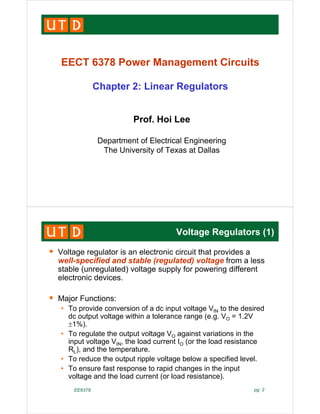
  • 1. EECT 6378 Power Management Circuits EECT 6378 Power Management Circuits Chapter 2: Linear Regulators p g P f H i L Prof. Hoi Lee Department of Electrical Engineering Department of Electrical Engineering The University of Texas at Dallas Voltage Regulators (1) Voltage regulator is an electronic circuit that provides a well-specified and stable (regulated) voltage from a less stable (unregulated) voltage supply for powering different ( g ) g pp y p g electronic devices. Major Functions: Major Functions: • To provide conversion of a dc input voltage VIN to the desired dc output voltage within a tolerance range (e.g. VO = 1.2V 1%) 1%). • To regulate the output voltage VO against variations in the input voltage VIN, the load current IO (or the load resistance R ) and the temperature RL), and the temperature. • To reduce the output ripple voltage below a specified level. • To ensure fast response to rapid changes in the input lt d th l d t ( l d i t ) EE6378 pg. 2 voltage and the load current (or load resistance).
  • 2. Voltage Regulators (2) DC voltage transfer function: O DC , v V V M where Mv,DC is the voltage conversion ratio IN DC , v V DC current transfer function: O I M Power efficiency of a dc-dc converter: IN O DC , I I I M DC , I DC , v IN O IN O in o M M I I V V P P EE6378 pg. 3 IN IN in Voltage Regulators (3) Static Characteristics: • Line regulation is the ratio of the output voltage change V t di h i th i t lt VO to a corresponding change in the input voltage ) V mV ( | ) V V ( LNR constant T and constant I O A O ) V ( | ) V ( constant T and constant I IN A O EE6378 pg. 4
  • 3. Voltage Regulators (4) Static Characteristics: • Load regulation is the ratio of the output voltage change V t di h i th l d t VO to a corresponding change in the load current ) A mV ( | ) I V ( LOR constant T and constant V O A IN A IO A IN EE6378 pg. 5 Voltage Regulators (5) D i Ch i i Dynamic Characteristics: Line transient response Load transient response EE6378 Lecture 2 H. Lee pg. 6
  • 4. Linear Regulator Linear regulator is used to describe an dc-dc regulator in which the voltage or current is controlled using transistors or other active devices as variable impedance elements. This t pe of reg lator is called the linear reg lator type of regulator is called the linear regulator because, in the early days, the power device is realized by transistor (BJT) and normally realized by transistor (BJT) and normally operates in the linear region, rather than in the saturation or cutoff region. If MOS transistor is g used as the power device, it will usually operate in the saturation (pinch-off) region, but the l t i till k li l t regulator is still known as a linear regulator EE6378 pg. 7 R l t b di id d i t t h t l t d Types of Regulators Regulators can be divided into two groups: shunt regulators and series regulators: A shunt regulator has a variable impedance element in parallel with the load. The regulator diverts current from the load and thus control the load voltage A series regulator has a variable impedance element A series regulator has a variable impedance element connected in series between the unregulated power source and the load. The voltage across the load is sensed and impedance of the series element varied so as to keep the load voltage constant EE6378 pg. 8 voltage constant
  • 5. Shunt Regulator The simplest way of shunt regulator uses the reverse p y g breakdown of a Zener diode. The breakdown voltage due to Zener breakdown mechanism has a negative (-ve) temperature coefficient while the breakdown voltage due temperature coefficient, while the breakdown voltage due to the avalanche multiplication has a positive (+ve) coefficient. At a breakdown voltage of 5V, both effects are ti d th t t t ffi i t i l t active and the net temperature coefficient is close to zero. Therefore, Zener diode is a good candidate for a voltage regulator. g EE6378 pg. 9 Zener Diode Characteristics e I I V V s z T z / ) 1 ( When the zener diode is forward biased, it acts as a normal diode: C VT o 27 at 26mV voltage thermal where When it is reversed biased, the current follows the diode equation until the diode undergoes zener breakdown (by tunneling) usually at a voltage of 6 - 7V The exact IV characteristic of a zener diode in reverse breakdown region has a rather complicated mathematical expression. For simplicity, it is modeled as a battery (Vzk) in series with a resistor (rz): z z zk z r I V V EE6378 pg. 10
  • 6. Zener Diode Regulator (1) The circuit of a simple zener diode regulator is as: (2) ) ( (1) ZK Z Z s L Z in ZK Z Z Z o V r I R I I V V r I V V We need to express Vo in terms of Vin, VZK and IL by (1) and (2): ( ) ) ( ZK Z Z s L Z in r R R r L z s z s ZK z s s in z s z o I r R r R V r R R V r R r V EE6378 pg. 11 Zener Diode Regulator (2) As zener diode current Iz > 0, the load current should be o in L R V V I z s z in o r R V r R r V V Regulation Line s R For good line and load regulations, both require a small rz which is <<Rs z s z s L o r R r R - I V Regulation Load The efficiency of the regulator is given as ) ( power input total power output ) ( Efficiency s L o L o V V V R I V ) I (I V I V The efficiency is the largest when the load current is maximum and the source voltage is minimum ) ( power input total o in in z L in V V V ) I (I V EE6378 pg. 12 source voltage is minimum
  • 7. Example Two-stage shunt regulator: Find the line and load regulations of above circuit where V =26V Find the line and load regulations of above circuit where Vin=26V. What are advantages of using the two-stage shunt regulator compared to the simple shunt regulator (without Rs2 and the second zener diode)? EE6378 pg. 13 Answers 2 t d i li l ti 2 77 V/V d 2-stage design: line regulation = 2.77mV/V and load regulation = -9.7V/A 1 stage design: line regulation = 90 9mV/V and 1-stage design: line regulation = 90.9mV/V and load regulation = -18.2V/A Two stage design improves both line and load Two-stage design improves both line and load regulations of the shunt regulation EE6378 pg. 14
  • 8. Series Regulator Series regulators have a variable impedance element between the source and the load. As the load current or source voltage varies, the impedance of the series element is adjusted to keep the output voltage constant. Therefore, the only current in the series element is the load current and its efficiency is given by circuitry control the in current supply the is I re whe ) ( q in o q o in o o V V I I V I V The efficiency does not depend on the load current, only on the ratio of load-to-source voltage. Series regulator is thus generally preferred load to source voltage. Series regulator is thus generally preferred compared to the shunt regulator. EE6378 pg. 15 Basic Concept (1) Using voltage-divider model, value of output voltage Vo p g o in p L L o V R R R V Vo can be maintained constant by changing the value of RP h R V b th h Voltage Divider Model when RL, Vin or both change Negative feedback control circuitry measures V and circuitry measures Vo and controls the value of Rp to achieve the desired Vo Linear Regulator Model EE6378 pg. 16
  • 9. Basic Concept (2) Power efficiency of the linear regulator L d i L I V V I V cont L L in do in in L in o V I I I ) V V V ( I I V V where V is the dropout voltage (V V ) and I is in do V V 1 where Vdo is the dropout voltage (Vin - Vo) and Icont is the current consumption of the controller. Normally, Icont << IL Icont IL To maximize , Vdo should be minimized (i.e. Rp should be much smaller than RL) EE6378 pg. 17 L) Structure of Series Regulator Vin Below is a typical series regulator which consists of four main building blocks: Vref Q1 Va A(s) V Vo Rf2 r V- Vfb R RL rc C Rf1 C EE6378 pg. 18
  • 10. Structure of Series Regulator (2) Voltage Reference (Vref): a very stable voltage with respect to temperature change and input voltage variations usually of the bandgap type variations, usually of the bandgap type. Error Amplifier (A(s)): a very high (dc) gain opamp to achieve a close to zero error signal Verr=V+-V-. Feedback Network: Rf1 and Rf2 define the feedback factor and generate Vfb to be compared with Vref to get the designed output voltage V the designed output voltage Vo. Series Pass/Power Transistor (Q1): power transistor configuration to pass high current from the source to output. As it handles large current, the size of pass transistor dominates the area of the whole series regulator. EE6378 pg. 19 regulator. Questions If Vref = 1.2V, Rf1 = 1M , Rf2 = 3M , what is the value of Vo? If VCE,sat,Q1 = 0.2V, what is the minimum input supply voltage of the linear regulator? linear regulator? If the offset voltage Voff of the error amplifier is 20mV what is the 20mV, what is the percentage change in the output voltage? Repeat this if input stage V ML M3 M4 V1 Repeat this if input stage of the error amplifier is PMOS transistors and Vref = 0.5V. Vo Mb1 Mb2 Mb3 M1 M2 Cm Vin EE6378 pg. 20 ref
  • 11. Answers Vo = Vref(1+Rf2/Rf1) = 1.2(1+3) = 4.8V by assuming dc gain of the error amplifier is very large. Vin,min = max(Vo+VBE,Q1+Vov,ML, Vo+VCE,sat,Q1) = Vo+VBE,Q1+Vov,ML = 4.8+0.7+0.15=5.65V. Vo’= (Vref+Voff)(1+Rf2/Rf1) = (1.22)(1+3) = 4.88V that corresponds to 1.67% increase in the output voltage. Therefore, it is very important to i i i th ff t f th lifi i d t i th f minimize the offset of the amplifier in order to improve the accuracy of the linear regulator. If Vref = 0.5V, then Vo = 2V and Vin,min = 2+0.7+0.15 = 2.85V. With 20mV offset of the error amplifier, Vo’ = 2.08V that corresponds to 4% increase in the output voltage. Therefore, the output voltage variation of the l t i h ll l f lt i d EE6378 pg. 21 regulator increases when a small-value reference voltage is used. Concerns of Series Regulator The linear regulator can only perform step down dc-dc The linear regulator can only perform step down dc dc conversion. i.e. Vo < Vin Since = Vo/Vin, with Vo = 5V and Vin = 10V, = 50%. Therefore, linear regulator has a very poor efficiency if the difference between Vo and Vin is large. The wasted the difference between Vo and Vin is large. The wasted power is mainly dissipated by the power transistor Q1 as heat. EE6378 pg. 22
  • 12. Concern of Using NPN Pass Transistor With a Li-Ion battery as Vin, Vin varies from 2.7V to 4.2V. The maximum output voltage of the linear regulator using NPN pass transistor is Vin,min-VBE,Q1-Vov,ML 2.7- 0.7-0.15 = 1.85. Efficiencies of linear regulator with V = 1 85V: Efficiencies of linear regulator with Vo = 1.85V: • max = Vo/Vin,min = 1.85/2.7 = 68.5%. • min = Vo/Vin max = 1.85/4.2 = 44%. min Vo/Vin,max 1.85/4.2 44%. Efficiency of the linear regulator using NPN transistor is very poor! Poor efficiency will also be resulted from using NMOS transistor as the pass transistor. EE6378 pg. 23 The linear regulator uses negative feedback loop to keep the output voltage constant with Principle of Operation (1) The linear regulator uses negative feedback loop to keep the output voltage constant with respect to the change of input supply and load current. Negative feedback loop consists of feedback resistors (Rf1 & Rf2), error amplifier and Q1 For example: when Io o Vo as load current is initially drawn from the output capacitor Vfb as Vfb = (Rf1/(Rf1+Rf2))Vo Va = A(Vref-Vfb) V (N i f db k V i i i i i l l ) Negative Feedback Vo (Negative feedback causes Vo to maintain its original value) Same reasoning explains why Vo can maintain a relatively constant value when IL decreases. EE6378 pg. 24
  • 13. Principle of Operation (2) When Vin Vo as collector current of Q1 increases Vfb as Vfb = (Rf1/(Rf1+Rf2))Vo V = A(V V ) Negative Va = A(Vref-Vfb) Vo (Negative feedback causes Vo to maintain its original value) Same reasoning explains why Vo can maintain a relatively constant value when Vin decreases. Feedback Vo ML M3 M4 C V1 EE6378 pg. 25 Mb1 Mb2 Mb3 M1 M2 Cm Vin Review on Feedback Theory Typical Feedback System Define: A – Open-loop gain b – Feedback factor L = Ab loop gain L = Ab – loop gain Af – Closed-loop gain 1+Ab – amount of feedback 1 Ab if 1 1 ) ( b Ab A x x A Abx Ax x x A Ax x i o f o i f i e o EE6378 pg. 26
  • 14. Linear Regulator as Feedback System (1) o o in a o R I V V V where Ro is the equivalent resistance at output o o in o ref o o in fb ref o o in a o R I V bV V A R I V V V A ) ( ) ( o o in ref o I Ab R V Ab V Ab A V 1 1 1 1 EE6378 pg. 27 Linear Regulator as Feedback System (2) o o in ref o I Ab R V Ab V Ab A V 1 1 1 1 on Based A V 1 b Ab A V V ref o 1 1 Larger b can improve the accuracy of the output voltage with respect to the variation of the reference voltage Ab Ab V V in o 1 1 1 with respect to the variation of the reference voltage. R V o o Line regulation is improved by the loop gain of feedback system. Larger dc loop-gain magnitude gives better line regulation. Ab Io 1 Load regulation is improved by the loop gain of feedback system. Larger dc loop-gain magnitude gives better load regulation. EE6378 pg. 28
  • 15. Loop-Gain Analysis (1) Break the loop and analyze the loop gain L(s) of linear regulator for stability. ) ( ) ( ) ( s V s V s L fb EE6378 pg. 29 Loop-Gain Analysis (2) Two assumptions: • Error amplifier has zero output resistance: va = -A(s)v- • Rf1, Rf2 >> R such that (Rf1+Rf2)//R R v v v v v v v v s L a a o o fb fb ) ( f1, f2 ( f1 f2) a L c L o v SC r R r SC r R v )] / 1 //( )[ 1 ( )] / 1 //( )[ 1 ( v v v v a o c L SC r R r )] / 1 //( )[ 1 ( ) 1 ( ) ( 1 ) 1 ( ) 1 ( L L c L o r R r R r sCr R r R v v ] ) 1 ( ) 1 ( ) ( [ 1 ) 1 ( L c L c L L a R r r R r R r sC R r v EE6378 pg. 30
  • 16. Loop-Gain Analysis (3) ] ) 1 ( ) 1 ( ) ( [ 1 1 ) 1 ( ) 1 ( L c L c L c L L a o R r r R r R r sC sCr R r R v v LHP zero z: 1/Crc; LHP Pole p: ] ) 1 ( ) 1 ( ) ( [ / 1 L c L c L R r r R r R r C • Since ESR of a large capacitor is usually very small such that rc can usually be neglected when compared to RL. For example: the ESR of a 10 F capacitor is as small as 50m . • The emitter resistance of the pass transistor is much smaller than the load resistance. For example: 1/gm << RL or r << (1+ )RL 1 ) 1 ( ) 1 ( ) ( L L L L r r R R r r R r R r ) / 1 ( 1 and 1 1 1 ) 1 ( ) 1 ( ) 1 ( ) 1 ( ) ( p m c c z c m c L c L L L c L c L g r C Cr r g r r R r R R r R r r R r R r EE6378 pg. 31 ) / 1 ( m c c g r C Cr Loop-Gain Analysis (4) z f o f fb s v s A R R R v R R R v / 1 / 1 ] ) ( [ 1 1 z f fb p f f o f f fb s R s A v s L s R R R R / 1 ) ( ) ( Therefore, / 1 1 2 1 2 1 p f f s R R s A v s L / 1 ) ( ) ( Therefore, 2 1 ) / 1 ( 1 and 1 where p z g r C Cr ) / 1 ( m c c g r C Cr The pole is located at lower frequency than that of zero. EE6378 pg. 32
  • 17. Loop-Gain Analysis (5) A( ) i th t f f ti f t d lifi A(s) is the transfer function of an uncompensated amplifier with a dominant pole 1 and a very high-frequency pole 2. Loop gain is always stable if z is located close to 1. EE6378 pg. 33 Loop gain is always stable if z is located close to 1. Concerns of Loop-Gain Compensation As mentioned before, z should be close to 1 for stability. There are concerns to allow z located at low frequency: frequency: • We can increase CL to push z to a lower frequency. However, the first pole of loop-gain function p also decreases. The unity- i b d idth f th l i f ti d d h gain bandwidth of the loop-gain function decreases and hence load transient response of linear regulator degrades. • We can increase rc to push z to a lower frequency by using a physical resistor in addition to the ESR of C However large r physical resistor in addition to the ESR of CL. However, large rc also significantly degrades the load transient response of the linear regulator. In practical situations, it is difficult to realize low- frequency z without suffering from the tradeoff. EE6378 pg. 34 frequency z without suffering from the tradeoff.
  • 18. Why Low-Dropout Regulator ? (1) With a Li-Ion battery as Vin, Vin varies from 2.7V to 4.2V. The maximum output voltage of the Vin p g linear regulator using NPN pass transistor is Vo,max= Vin,min-VBE,Q1- Vov,ML 2.7-0.7-0.15 = 1.85 in order Vref Vo Q1 Va A(s) V- to allow the linear regulator to function properly Dropout Voltage (Vdo) is the o Vfb Rf2 RL rc minimum voltage difference between the input and output under which the regulator still able to maintain the o tp t ithin Rf1 RL C able to maintain the output within the specification In this case, Vdo,max = 4.2-1.85 = 2 35V EE6378 pg. 35 2.35V Why Low-Dropout Voltage ? (2) As mentioned before, efficiencies of linear regulator with V =1 85V can be as low as Vo=1.85V can be as low as • min = Vo/Vin,max = Vo/(Vo+Vdo,max) = 1.85/(1.85+2.35) = 44% For portable equipment, a 2.35V dropout voltage is not efficient. To solve this problem, a low-dropout voltage p , p g regulator (LDO or LDR) is designed to allow the input voltage to go down to a very low value above Vo by changing the pass transistor from NPN/NMOS changing the pass transistor from NPN/NMOS transistor to PNP/PMOS transistor. EE6378 pg. 36
  • 19. Choice of Power Transistor (1) Using nMOS as Rp • Smaller power device size to handle the same load Using pMOS as Rp Good power efficiency as Vdo is independent of V (Low to handle the same load current • Poor power efficiency due f is independent of Vg (Low- dropout regulator) Low frequency pole at node V d d th t bilit EE6378 pg. 37 to large Vdo if Vg Vin Vg degrades the stability Choice of Power Transistor (2) Different Vg maintains the fixed Vo by varying Vdo under different V and fixed I Different Vg maintains the fixed Vo under different It (both V and V are fixed) Power device Mp can operate either in the triode region or saturation region! different Vin and fixed It (both Vin and Vdo are fixed) W 1 1 W ) V 1 ( ) V V V ( L W C 2 1 I do 2 th o g ox t EE6378 pg. 38 ) V 2 1 V ) V V V ( L W C I 2 do do th o g ox t
  • 20. Structure of LDO Design Issues: • Power PMOS transistor • Error Amplifier • Rf1 and Rf2 made of the same material • Voltage Reference • Stability and speed of feedback loop EE6378 pg. 39 y • Choice of output off-chip capacitor Specifications of LDO Two Categories: • Regulating (accuracy) performance Line regulation, load regulation, temperature dependence, transient overshoot, transient recovery time, stability • Power Characteristics Io, Quiescent current Iq, Vin & Vo ( & I) EE6378 pg. 40
  • 21. Efficiency (1) C t Effi i Current Efficiency I: I = Io/(Io+Iq) where Iq is the quiescent current of LDO Iq=I1+I2+I3 In LDO design for portable applications I is usually much larger than I with In LDO design for portable applications, Io is usually much larger than Iq with > 99% efficiency When Io is 0, Iq should be minimized (I3 should be small by using large values of Rf1 and Rf2) EE6378 pg. 41 Efficiency (2) 1 do o o o o V V I V P - 1 ) ( 3 2 1 in do in o o in o o in o V V V V I I I I V I V P P Smaller dropout voltage causes a higher power conversion efficiency especially Io >> Iq In light-load condition (small Io), the efficiency is poorer as I1, I2, and I3 are close to Io EE6378 pg. 42
  • 22. Dropout Voltage and Power-Transistor Sizing ) / ( 2 where L W C I V o ov ) / ( L W Cox p VSD is larger than Vov to allow LDO operating in the SD ov saturation region Design at the worst case: largest Vov at Io(max) and p(min) at the maximum temperature ( By using minimum L (the smallest transistor and hence parasitic capacitance), keep increasing W until meeting the dropout specification IR at the routing metals increase V IR at the routing metals increase VDO Design margin by experience-generally the chosen W is 1.1-1.2 times of the theoretical W EE6378 pg. 43 Load Regulation Vref A(s) L R I V R o L o 1 Vin RL rc Rf2 Vfb Vo L C Rf1 Load Regulation (R): closed-loop output resistance of LDO Ro is the open-loop output resistance of the pass transistor as Rf1, Rf2 >> Ro Rf1, Rf2 Ro Better load regulation is achieved by smaller Ro (using minimum channel length of the pass transistor) and larger loop-gain magnitude EE6378 pg. 44 As Ro 1/Io, high Io range gives better load regulation
  • 23. Line Regulation I Vref A(s) V L R I V R o L o 1 in o mp V I g Vin+ Vin RL rc Rf2 Vfb Vo A R g R V PT o mp o 1 C Rf1 b A b A A A L g R g V V PT PT o mp mp in o 1 1 1 gmp is the transconductance of power PMOS transistor Line regulation is independent of the gain of the power transistor Line regulation can be improved by a high-gain error amplifier Other error sources on line regulation are voltage reference and ff t lt f th lifi EE6378 pg. 45 offset voltage of the error amplifier Review on Voltage Gain Vin Transconductance Cell (Gm) Vo Io Ro i o m v i G in o o o m in o v R i R G v v Gain Stage in v in in v v Gm and Ro can be found individually Input-Output voltage gain can be found by the product of Gm and p p g g y p m Ro EE6378 pg. 46
  • 24. Line Regulation Including Other Errors o I Vref A(s) V L R I V R o L o 1 in o mp V I g Vin+ Vin Vref Vos RL rc Rf2 Vfb Vo 1 V V R V C Rf1 ) )( 1 ( 1 1 2 in os in ref f f in o V V V V R R b A V V LDO feedback loop Error amp. and Vref Voltage gain of the error amplifier is not the only parameter to improve line regulation Good designs on supply independence of Vref and reducing EE6378 pg. 47 g pp y p ref g systematic offset of error amplifier are very important Temperature Coefficient I Vref A(s) L R I V R o L o 1 in o mp V I g Vref Vos Vin RL rc Rf2 Vfb Vo os L C Rf1 ) )( 1 ( 1 2 T V T V R R T V os ref f f o V i ti f V t diff t t t d d b th lt Variation of Vo at different temperature depends on both voltage reference and error amplifier design Rf1 and Rf2 must be made by the same material and closely placed EE6378 pg. 48 placed
  • 25. Load Transient Response (1) Note that: • Re = rc (previous notes) • Co = C (previous notes) EE6378 pg. 49 Load Transient Response (2) Better load transient response by tresp , Co , Re and Lc . EE6378 pg. 50
  • 26. AC Design (1): Loop-Gain Analysis ) R R R ( ) C sR 1 ( z R g g | V V | L 2 1 1 pa a o a mp ma n fb o L(s) = Vfb/Vn = loop gain of the LDO Lo = |Vfb/Vn| = loop-gain magnitude (Vfb/Vn) = phase of loop gain that starts at 180o t t i d t V EE6378 pg. 51 zo = output impedance at Vo AC Design (2): Loop-Gain Analysis o o e x o sC C sR r z 1 // L o x R R R r r // ) //( 2 1 L o R R R r ) ( 2 1 In no-load condition, IL=0 Note: ) ( 2 1 R R R r L o In heavy-load condition, IL>>0 ro is the output resistance of power transistor Mp o x r r In both conditions o x o o e o o o C sr R sC r z 1 ) 1 ( EE6378 pg. 52
  • 27. AC Design (3): Loop-Gain Analysis ) R R R ( ) C sr 1 )( C sR 1 ( ) C sR 1 ( r r g g | V V | L 2 1 1 o o pa a o e o a mp ma n fb o The system has 2 poles and 1 zero o oC r p 1 1 1 pa a 2 C R 1 p 1 o e e C R z 1 EE6378 pg. 53 AC Design (4): Loop-Gain Analysis ze should cancel p2 within one decade of frequency for stability Parasitic pole(s), ppar, must be far away p from the unity-gain frequency (UGF) Different UGFs are resulted from different Re values such as ze locating before or after p2 p2 locates at very low frequency as Cpa and Ra are large Required large Co and Re • Large Co decreases the unity-gain frequency • Large Re degrades load transient response • Low-frequency pole-zero cancellation is f bl t l d t i t EE6378 pg. 54 unfavorable to load transient recovery time
  • 28. LDO with Voltage Buffer Smaller required Re can be achieved by inserting a low output- resistance (1/gmb) voltage buffer ( gmb) g One more pole (p3) is created but is located at high frequency due to small output resistance of the voltage buffer p2 (with voltage buffer) locates at a higher frequency than the one EE6378 pg. 55 p2 (with voltage buffer) locates at a higher frequency than the one without voltage buffer (Cb << Cg) Effect of Load Currents on Stability L i i ll h I Loop gain is smaller when Io becomes larger due to gmpro 1/ Io p1 is moved to a higher frequency at a faster rate than the decrease in loop gain magnit de hen I in loop-gain magnitude when Io increases due to smaller ro of the power transistor (ro 1/Io) Hence, Distance between p1 and p2 becomes smaller when Io increases and the worst case increases and the worst-case stability occurs at maximum Io C EE6378 pg. 56 Compensation is needed at max. Io
  • 29. Effect of Loop-Gain Magnitude on Stability Larger loop gain by increasing Ra of the error amplifier p2 p2’ A l R i d d t t A larger Re is needed to create a zero at lower frequency (ze ze’) Larger loop gain more unstable as p3 may be below the UGF of loop gain A larger Co is generally needed EE6378 pg. 57 Loop Gain Simulation L(j )=Vfb(j )/Vn(j ) Information lower than 1/( LxCx) is not valid EE6378 pg. 58
  • 30. Summary of LDO Specifications Specifications Approaches for Improvement Stability Lo and UGF Output voltage error due to finite loop gain Lo Line regulation Lo g o Load regulation Lo T i t UGF , PM , SR , Co and Transient response , , , o ESR Where L = loop gain magnitude UGF = unity gain frequency of the loop gain response Lo = loop-gain magnitude, UGF = unity-gain frequency of the loop-gain response, PM = phase margin of the loop-gain response, SR = slew rate at the gate of the power transistor, Co = off-chip output capacitor, ESR = equivalent series resistance of the off-chip output capacitor EE6378 pg. 59 Circuit Implementations (1) Mb2 Mp Mb2 Me1 Circuit of LDO consists of • R1 and R2 • Cin and Co • V f Vref • Error Amplifier • Voltage Buffer • Power Transistor V V V V EE6378 pg. 60 Vin,min = Vov,Me1 + Vgs,Mb2 + Vgs,Mp
  • 31. Circuit Implementations (2) BJT has a small VBE drop (~0.7V) The circuit can operate at lower input supply compared to the previous case previous case Smaller input capacitance for small VBE Base current introduces larger offset voltage and hence degrades f h l EE6378 pg. 61 accuracy of the output voltage Circuit Implementations (3) Vthn << |Vthp| is needed to turn off the power PMOS transistor effectively when Io=0 Some circuit uses npn BJT transistor instead, but non-zero current is a problem and npn BJT transistor is not available in standard n-well CMOS technologies EE6378 pg. 62
  • 32. Circuit Implementations (4) Better matching by BJT Non-zero base current, but micro-ampere collector current with a large current gain large current gain Better input common-mode range NPN BJT transistor is unavailable in standard n-well CMOS technologies EE6378 pg. 63 technologies Review on Device Matching Matching of Using NPN Input Pair ) ) / ( ) / ( ( ) ( ) ( , p T mp thp npn s T os L W L W V g g V I I V V Matching of Using NMOS Input Pair ) / ( , , p BJT m p npn s L W g I ) ) / ( ) / ( ) / ( ) / ( ( 2 ) ( ) ( , p p n n thn n gs mn mp thp thn os L W L W L W L W V V g g V V V VT = thermal voltage of BJT transistor 26mV, gm,BJT >> gmn under the same bias current V (V V ) h (V V ) 150 V VT << (Vgs,n – Vthn) where (Vgs,n – Vthn) 150mV mV V mV I I V thn npn s npn s T 10 4 ) ( , , EE6378 pg. 64
  • 33. Circuit Implementations (5) Limited output swing causes limited Vgs of the power PMOST A large transistor size is therefore required Few pairs of device to match lower random offset voltage EE6378 pg. 65 Few pairs of device to match lower random offset voltage Pros & Cons of Linear Regulators Advantages: • Simple structure which can be fabricated on a single chip • Very few external components needed May need as few as only • Very few external components needed. May need as few as only the input and output filtering capacitors • For system design, very easy to use. The IC may have only 3 pins V V and GND pins, Vin, Vo and GND • Small output ripple, good line and load regulations • Apparently no electromagnetic interference (EMI) problem Disadvantages: • Very low efficiency which is limited to V /V if V is large • Very low efficiency which is limited to Vo/Vin if Vdo is large • May need bulky heat sink to dissipate waste heat • Vo has to be lower than Vin. i.e. step down only EE6378 pg. 66
  • 34. Protection Circuitries It is important when designing linear regulators is protection against undesirable factors that are inherent p g to the working environment of the application. As the power pass device dissipates most power, protection usually revolves around its operating protection usually revolves around its operating conditions. Operating limits are defined by power dissipation, output current range, breakdown voltage, temperature ratings, etc. Overload protection (current limiting) and thermal shutdown are two most common methods to protect shutdown are two most common methods to protect power pass transistor. EE6378 pg. 67 Structure of Linear Regulator with Protection Structure of linear regulator adopting both over Structure of linear regulator adopting both over- current protection and thermal shutdown: EE6378 pg. 68
  • 35. Overload Protection A frequent occurrence of overload is to short the output node Vo to ground. For example, if specifications limit the maximum output current 200mA the minimum load maximum output current 200mA, the minimum load resistor is 10 for Vo = 2V. It is understandable that an user of the linear regulator accidentally placing a 5 at th t t f th li l t l d the output of the linear regulator can cause overload condition. Therefore overload protection is important. The most effective way to prevent overload is to steal the The most effective way to prevent overload is to steal the base current of the power transistor. • The protection consists of Rsc and Q3. Rsc is a low resistance high power resistor (e g 0 1 with power rating of 10W) high power resistor (e.g. 0.1 with power rating of 10W) • When Io , VRsc . When VRsc=VBE3(on)=0.7V, Q3 turns on and steals IB from the power transistor I i li it d t I V /R EE6378 pg. 69 • Io is limited to Isc = VBE3(on)/Rsc Thermal Shutdown (1) When large current passes though the power transistor Q1 excess heat will raise the junction temperature T of Q1, excess heat will raise the junction temperature Tj of Q1. When Tj = 150 C (or 175 C), Q1 breaks down and will be damaged permanently. The thermal shutdown circuit consists of R7, R8 and Q4. R and R form a voltage divider with V = 0 4V R7 and R8 form a voltage divider with VBE4 = 0.4V. Therefore, Q4 is OFF at room temperature. Therefore, R7, R8 and Q4 will not affect the circuit operation at room temperature. EE6378 pg. 70
  • 36. Thermal Shutdown (2) Assume VBE4(on)(25 C) = 700mV and the tempco of VBE is around -2mV/ C. At 175 C, VBE4(on)(175 C) = 700mV-(2mV)(175-25) = 400mV. Further increase in temperature above 175 C p will turn on Q4 hard, stealing base current from the pass transistor. As a result, the load current decreases and heat generated from Q1 will decrease. g Q4 should have excellent thermal coupling with Q1. In addition V is a bandgap reference and the reference addition, Vref is a bandgap reference and the reference voltage will become more or less constant over wide range of temperature. EE6378 pg. 71 Some Related References G. A. Rincon-Mora, et. al., “A low-voltage, low quiescent current, low dropout regulator,” IEEE JSSC, pp. 36-44, Jan. 1998. p g pp G. A. Rincon-Mora, et. al., “Active capacitor multiplier in Miller- Compensated Circuits,” IEEE JSSC, pp. 26-32, Jan. 2000. K. N. Leung, et. al., “A capacitor-free CMOS low-dropout regulator K. N. Leung, et. al., A capacitor free CMOS low dropout regulator with damping-factor-control frequency compensation,” IEEE JSSC, pp. 1691-1702, Oct. 2003. P. Hazucha et. al., “Area-efficient linear regulator with ultra-fast load P. Hazucha et. al., Area efficient linear regulator with ultra fast load regulation,” IEEE JSSC, pp. 933-940, Apr. 2005. M. Al-Shyoukh et. al., “A transient-enhanced low-quiescent current low-dropout regulator with buffer impedance attenuation,” IEEE low dropout regulator with buffer impedance attenuation, IEEE JSSC, pp. 1732-1742, Aug. 2007. EE6378 pg. 72