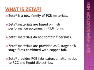
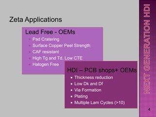
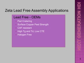
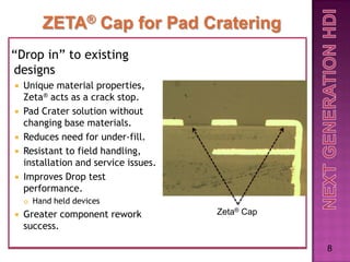
Zeta® For
Printed Circuit
Boards


                  1
Technical Support for the
      family of businesses

-     Technical Services
-     Research & Development
-     Field Installations
-     Process Development
-     Process Audits
-     Defect Analysis
 Zeta®   is a new family of PCB materials.

 Zeta®materials are based on high
 performance polymers in FILM form.

 Zeta®   materials do not contain fiberglass.

 Zeta®materials are provided as C stage or B
 stage films combined with copper foil.

 Zeta® providesPCB fabricators an alternative
 to RCC and liquid dielectrics.
                                                 3
Zeta Applications
     Lead Free - OEMs
         Pad Cratering
         Surface Copper Peel Strength
         CAF resistant
         High Tg and Td, Low CTE
         Halogen Free
                          HDI – PCB shops+ OEMs
                               Thickness reduction
                               Low Dk and Df
                               Via Formation
                               Plating
                               Multiple Lam Cycles (>10)
                                                            4
Zeta Lead Free Assembly Applications
    Lead Free - OEMs
        Pad Cratering
        Surface Copper Peel Strength
        CAF resistant
        High Tg and Td, Low CTE
        Halogen Free


                                        5
PAD “CRATERING”
   Mechanically induced fracture in the resin between copper foil and
     outermost layer of fiberglass. May be within the resin or at the
     resin to glass interface.
   Pad remains connected to the component (usually BGA) and leaves a
     “Crater” in the PCB.


                                                                         6
PAD “CRATERING” = Opens
 Fractures start in the dielectric (resin) and works through the
copper trace creating an open circuit.


                                                                    7
ZETA® Cap for Pad Cratering
“Drop in” to existing
designs
   Unique material properties,
    Zeta® acts as a crack stop.
   Pad Crater solution without
    changing base materials.
   Reduces need for under-fill.
   Resistant to field handling,
    installation and service issues.
   Improves Drop test
    performance.
       Hand held devices
   Greater component rework           Zeta® Cap
    success.

                                                   8
Modulus kpsi (strength)   % Elongation (flexibility)
4500                                                                            80


4000                                                                            70

3500
                                                                                60

3000
                                                                                50

2500
                                                 Zeta Cap                       40
2000                                             Is more flexible than rigid,
                                                 but 3 times stronger than      30
1500                                             flex. This prevents
                                                 fractures from starting.
                                                                                20
1000


 500                                                                            10


   0                                                                            0

       Kapton              Zeta Cap          epoxy               polyimide

                                                                                     9
 Copper
    ¼ oz (9 µm), 3/8 oz (12 µm), ½ oz (18 µm)
    Low tooth profile
    6 to 7 pound peel strength
    RTF finish
C   stage Dielectric
    0.5 mil (12 µm), 1.0 mil (25 µm), 1.5 mil (38 µm)
    Non-copper side treated for prepreg bonding
    Tg > 300⁰C, Td > 500⁰C
    @ 2GHz – Dk = 3.0, Df = .005
    Dielectric Strength – 4900 v/mil
    Halogen Free
                                                         10
 UL
    94-V0, MOT 155⁰C
 Pad   Crater Testing
    1.0 mil with Pad Crater TV, hot pin pull test with OEM #1
    Prototype boards built with 0.5 and 1.0 mil with OEM #1
    Pad Crater TV PCBs under construction for OEM #2
    Pad Crater TV design completed for OEM #3, PCB
     construction to follow.


                                                                 11
   Questions regarding Zeta® lead free assembly applications?


                                                                 12
Zeta HDI Applications

 HDI – PCB shops+ OEMs
     Thickness reduction
     Low Dk and Df
     Via Formation
     Plating
     Multiple Lam Cycles (>10)


                                  13
ZETA® C STAGE/ B STAGE PRODUCTS
   Zeta® Cap
     Copper clad high Tg, low CTE fully
      cured dielectric.
     Used with standard prepregs or
      Zeta® Bond.

   Zeta® Bond
     Hi Tg “B” stage film that is glass free.
     Thickness is easily tailored to fill
      areas around plated circuits.
     Hi peels, even after multiple lam
      cycles.

   Zeta® Lam
       Zeta® Cap + Zeta® Bond
       Ready to use in Lay-up without Prepreg

                                                 14
 New     epoxy technology for multiple lam cycles
     Non-dicy
     Non-phenolic
 Room  temp storage
 High Tg and High Td
 High flow and fill
 Low moisture absorbing
     Tg after 72 hours in boiling water- 174⁰C
     Moisture uptake @ 72 hours in boiling water – 1.0%
     Moisture uptake for Kapton, 24 hrs room temp -2.8%
 Requires change      in press cycle
     Start temp is 350⁰F instead of 200 - 250⁰F
                                                           15
 Epoxy    based high density crosslinking resin
     Requires more heat to gel
     Much longer shelf life - > 1 year
     Does not require refrigeration
     Non-brittle B stage
     Halogen free and not brittle after cure
 350⁰F to gel in 15 minutes
 375 ⁰F for 90 minutes to cure


                                                   16
ZETA® LAM
   Zeta® LAM
       C-stage layer provides a polymer solution for glass fabric;
           Consistent thickness control after lamination
           Very high dielectric strength
           Lower Z-axis CTE than other glass free dielectrics materials
           Lower Dk, Lower loss
           High copper peels at high temperatures
       B-stage layer provides;
           Bonding and fill of circuits and vias
               Various thicknesses of resins are available for fill requirements
           Curable with standard PCB laminating equipment (375ºF)
           Long shelf life, 1 year at room temperature
       IPC-4563
           Example –
            Zeta Lam C25EP/B38E TSL AA
            =1/3 oz copper + 1.0 mil “C” stage polyimide +1.5 mils of “B” stage epoxy
                                                   Copper
                                             C-Stage Polyimide

                                             B-Stage Epoxy

                                                                                        17
ZETA® LAM
   Zeta® LAM
       Available Coppers
           ¼ oz (9 micron)
           3/8 oz (12 micron)
           ½ oz (18 micron)
       C-stage layer
           ½ mil (12 micron)
           1 mil (25 micron)
           1.5 mil (38 micron)
       B-stage layer
           1 mil (25 micron)
           1.5 mil (38 micron)
           2.0 mil (50 micron)


                                       Copper
                                   C-Stage Polyimide

                                   B-Stage Epoxy

                                                       18
 Sequential        lamination
     Starts with double sided core
     Materials can be
         Prepreg
         RCC
         Photo dielectric (liquid and film)
         Screenable liquid
 Parallel      lamination
     Process is used for thru hole multilayers
     For Any Layer HDI, z-axis interconnects might be;
         Conductive Ink
         Copper posts/cones
 “Subs”       (cannot produce “Any Layer”)
     Combination of sequential and parallel
                                                          19
 Sequential        lamination
     Advantages
         “Any Layer” HDI capable
         Uses standard PCB processing
         Thin structures possible
     Disadvantages
         Requires multiple laminations
 Parallel      lamination
     Advantages
         High layer count possible with one lamination cycle
     Disadvantages
         Z-axis interconnect must be formed prior to lamination
         May require special process/equipment/materials
         Very thin layers (< 2 mil/50µ) hard to handle

                   Zeta can be used in both applications!          20
 Finer     copper traces are great for HDI
    But harder to produce with high yield
    As thickness gets reduced, so does Impedance
        To maintain the same Impedance;
        Line width must be reduced, or…
        Dk is reduced, this has the same effect.
        Zeta produces the same Impedance at half the
         thickness with the same line width.
    Thinner structures at the same Impedance have;
        Easier to drill and plate vias
        Lower via inductance
        Lower thermal impedance.

                                                        21
Zeta ®   for stacked vias


               Sequential lamination is a
               popular way to make HDI
               structures. This requires one
               lamination cycle for each
               layer.


                                               22
Thermal stress coupon


0.008” core + 9 layers
of Zeta® Lam on each
side.


20 layers


Overall thickness
0.035”


                         23
24
 Zeta® Bond SE
used to fill the via

 Testing applications
eliminating the via fill
process steps

 Zeta® Bond SE
resin available in
thicknesses to meet
many designs in filling
via’s

 Glass free allows
for more resin to flow
into vias


                           25
 FirstZeta Lam boards built and shipped
  February 2009, East Coast PCB shop

 Zeta Lam boards shipped in October 2009,
  West Coast PCB shop.

 Zeta Lam boards shipped by another West
  Coast PCB shop in March of 2009.

 Zeta Lam boards built and shipped from Bay
  Area PCB shop for ongoing design with “Any
  Layer HDI” using 9 lamination cycles.
                                               26
 Zeta   Cap has 94-V0 rating

 Zeta   Cap has MOT of 155⁰C

 Zeta Lam/Bond       SE flame testing in process
    94-V0 expected


 Zeta Lam/Bond       MOT should be 155 ⁰C


                                                    27
 IPC-4563
    Resin coated copper (RCC)
    Many items are AABUS (as agreed between user and supplier)
    Cover C-stage/B-stage combinations
    Spec allows for many different product types
    This is the best fit for Zeta® Lam and ZRC


 IPC-JPCA-4104
    High Density Interconnect (HDI) and Micro Via materials
        Covers dielectrics, foils and z-axis connections
        Includes many different types of materials
        Does not specify C-stage/B-stage combinations

                                                                  28
ZETA MATERIALS HAVE EXCELLENT THERMAL
              PROPERTIES FOR   GLASS FREE FILMS
 Material         Tg       Td      Z-axis CTE    Comments
 Zeta Cap       >300⁰C   >500⁰C     19 ppm/⁰C    Glass free film


 Zeta Bond       180⁰C    400⁰C     60 ppm/⁰C    Glass free film
    SE
Zeta Lam SE      N/A       N/A      40 ppm/⁰C    Glass free film

Dicy cured       180⁰C    300⁰C     55 ppm/⁰C        Glass
                                                  re-enforced
Hi Tg epoxy                                       0.020” core


 Phenolic        180⁰C    340⁰C     45 ppm/⁰C        Glass
                                                  re-enforced
  Epoxy                                           0.020” core
Flex Epoxy       100⁰C    285⁰C    >150 ppm/⁰C   Glass free film
 Bonding
   Film
                                                                   29
ZETA MATERIALS HAVE EXCELLENT ELECTRICAL
            PROPERTIES FOR GLASS FREE FILMS

 Material        Dk      Df     Breakdown     Comments
              (2 GHz)             Voltage
 Zeta Cap       3.0     0.005   4900 v/mil    Glass free film


 Zeta Bond      3.2     0.010   2500 v/mil    Glass free film
    SE
Zeta Lam SE     3.2     0.010   4900 v/mil    Glass free film

Dicy cured      4.2     0.014   1000 v/mil   Glass re-enforced
                                                0.020” core
Hi Tg epoxy

 Phenolic       4.0     0.021   1350 v/mil   Glass re-enforced
                                                0.020” core
  Epoxy
Flex Epoxy      3.2     0.020   3840 v/mil    Glass free film
 Bonding
   Film
                                                                 30
Thermal Conductivity    Thermal Resistance
  Manufacturer           Part
                                              (W/mK)                (˚C cm2/W)

Berquist         MP-06503                                 *1.3                   0.58
                 HT-04503                                 *2.2                   0.32
                 HT-07006                                 *2.2                   0.71
                 CML-11006                                *1.1                   1.35
Laird            T-LAM SS 1KA04                             *3                   0.34
                 T-LAM SS 1KA06                             *3                   0.52
                 T-LAM SS 1KA08                             *3                   0.70
                 T-LAM SS HTD04                           *2.2                   0.46
                 T-LAM SS HTD06                           *2.2                   0.69
Integral Tech.   Zeta Bond 1 mil                        **0.58                   0.44
                 Zeta Cap 1 mil                         **0.43                   0.59
Isola            370HR 106                              **0.44                   1.35
                 406 106                                **0.28                   2.12
Dupont           FR 1 mil                               **0.36                   0.71
                 Kapton 1 mil                           **0.14                   1.82
                 LF 1 mil                               **0.22                   1.16
                 CooLam LX03517016                        *0.8                   0.25
                 CooLam LX07022016                        *0.8                   0.29


                                * values sited from manufacturers data sheet
                                ** values from independent lab testing on “C” stage
   Questions regarding Zeta® HDI applications?


                                                  32
ZETA® HAS TWO BROAD BASE APPLICATIONS
      PAD CRATER FIX
      HDI
AS OF NOW, PAD CRATERING HAS NO OTHER FIX
We are being told this by many OEM’s
ZETA® FOR HDI
      MANY COMBINATIONS, APPLICATIONS POSSIBLE
      BE CREATIVE! SAMPLES ARE AVAILABLE!

                                                 33

Zeta 2 15-11

  • 1.
  • 2.
    Technical Support forthe family of businesses - Technical Services - Research & Development - Field Installations - Process Development - Process Audits - Defect Analysis
  • 3.
     Zeta® is a new family of PCB materials.  Zeta®materials are based on high performance polymers in FILM form.  Zeta® materials do not contain fiberglass.  Zeta®materials are provided as C stage or B stage films combined with copper foil.  Zeta® providesPCB fabricators an alternative to RCC and liquid dielectrics. 3
  • 4.
    Zeta Applications Lead Free - OEMs  Pad Cratering  Surface Copper Peel Strength  CAF resistant  High Tg and Td, Low CTE  Halogen Free HDI – PCB shops+ OEMs  Thickness reduction  Low Dk and Df  Via Formation  Plating  Multiple Lam Cycles (>10) 4
  • 5.
    Zeta Lead FreeAssembly Applications Lead Free - OEMs  Pad Cratering  Surface Copper Peel Strength  CAF resistant  High Tg and Td, Low CTE  Halogen Free 5
  • 6.
    PAD “CRATERING”  Mechanically induced fracture in the resin between copper foil and outermost layer of fiberglass. May be within the resin or at the resin to glass interface.  Pad remains connected to the component (usually BGA) and leaves a “Crater” in the PCB. 6
  • 7.
    PAD “CRATERING” =Opens  Fractures start in the dielectric (resin) and works through the copper trace creating an open circuit. 7
  • 8.
    ZETA® Cap forPad Cratering “Drop in” to existing designs  Unique material properties, Zeta® acts as a crack stop.  Pad Crater solution without changing base materials.  Reduces need for under-fill.  Resistant to field handling, installation and service issues.  Improves Drop test performance.  Hand held devices  Greater component rework Zeta® Cap success. 8
  • 9.
    Modulus kpsi (strength) % Elongation (flexibility) 4500 80 4000 70 3500 60 3000 50 2500 Zeta Cap 40 2000 Is more flexible than rigid, but 3 times stronger than 30 1500 flex. This prevents fractures from starting. 20 1000 500 10 0 0 Kapton Zeta Cap epoxy polyimide 9
  • 10.
     Copper  ¼ oz (9 µm), 3/8 oz (12 µm), ½ oz (18 µm)  Low tooth profile  6 to 7 pound peel strength  RTF finish C stage Dielectric  0.5 mil (12 µm), 1.0 mil (25 µm), 1.5 mil (38 µm)  Non-copper side treated for prepreg bonding  Tg > 300⁰C, Td > 500⁰C  @ 2GHz – Dk = 3.0, Df = .005  Dielectric Strength – 4900 v/mil  Halogen Free 10
  • 11.
     UL  94-V0, MOT 155⁰C  Pad Crater Testing  1.0 mil with Pad Crater TV, hot pin pull test with OEM #1  Prototype boards built with 0.5 and 1.0 mil with OEM #1  Pad Crater TV PCBs under construction for OEM #2  Pad Crater TV design completed for OEM #3, PCB construction to follow. 11
  • 12.
    Questions regarding Zeta® lead free assembly applications? 12
  • 13.
    Zeta HDI Applications HDI – PCB shops+ OEMs  Thickness reduction  Low Dk and Df  Via Formation  Plating  Multiple Lam Cycles (>10) 13
  • 14.
    ZETA® C STAGE/B STAGE PRODUCTS  Zeta® Cap  Copper clad high Tg, low CTE fully cured dielectric.  Used with standard prepregs or Zeta® Bond.  Zeta® Bond  Hi Tg “B” stage film that is glass free.  Thickness is easily tailored to fill areas around plated circuits.  Hi peels, even after multiple lam cycles.  Zeta® Lam  Zeta® Cap + Zeta® Bond  Ready to use in Lay-up without Prepreg 14
  • 15.
     New epoxy technology for multiple lam cycles  Non-dicy  Non-phenolic  Room temp storage  High Tg and High Td  High flow and fill  Low moisture absorbing  Tg after 72 hours in boiling water- 174⁰C  Moisture uptake @ 72 hours in boiling water – 1.0%  Moisture uptake for Kapton, 24 hrs room temp -2.8%  Requires change in press cycle  Start temp is 350⁰F instead of 200 - 250⁰F 15
  • 16.
     Epoxy based high density crosslinking resin  Requires more heat to gel  Much longer shelf life - > 1 year  Does not require refrigeration  Non-brittle B stage  Halogen free and not brittle after cure  350⁰F to gel in 15 minutes  375 ⁰F for 90 minutes to cure 16
  • 17.
    ZETA® LAM  Zeta® LAM  C-stage layer provides a polymer solution for glass fabric;  Consistent thickness control after lamination  Very high dielectric strength  Lower Z-axis CTE than other glass free dielectrics materials  Lower Dk, Lower loss  High copper peels at high temperatures  B-stage layer provides;  Bonding and fill of circuits and vias  Various thicknesses of resins are available for fill requirements  Curable with standard PCB laminating equipment (375ºF)  Long shelf life, 1 year at room temperature  IPC-4563  Example – Zeta Lam C25EP/B38E TSL AA =1/3 oz copper + 1.0 mil “C” stage polyimide +1.5 mils of “B” stage epoxy Copper C-Stage Polyimide B-Stage Epoxy 17
  • 18.
    ZETA® LAM  Zeta® LAM  Available Coppers  ¼ oz (9 micron)  3/8 oz (12 micron)  ½ oz (18 micron)  C-stage layer  ½ mil (12 micron)  1 mil (25 micron)  1.5 mil (38 micron)  B-stage layer  1 mil (25 micron)  1.5 mil (38 micron)  2.0 mil (50 micron) Copper C-Stage Polyimide B-Stage Epoxy 18
  • 19.
     Sequential lamination  Starts with double sided core  Materials can be  Prepreg  RCC  Photo dielectric (liquid and film)  Screenable liquid  Parallel lamination  Process is used for thru hole multilayers  For Any Layer HDI, z-axis interconnects might be;  Conductive Ink  Copper posts/cones  “Subs” (cannot produce “Any Layer”)  Combination of sequential and parallel 19
  • 20.
     Sequential lamination  Advantages  “Any Layer” HDI capable  Uses standard PCB processing  Thin structures possible  Disadvantages  Requires multiple laminations  Parallel lamination  Advantages  High layer count possible with one lamination cycle  Disadvantages  Z-axis interconnect must be formed prior to lamination  May require special process/equipment/materials  Very thin layers (< 2 mil/50µ) hard to handle Zeta can be used in both applications! 20
  • 21.
     Finer copper traces are great for HDI  But harder to produce with high yield  As thickness gets reduced, so does Impedance  To maintain the same Impedance;  Line width must be reduced, or…  Dk is reduced, this has the same effect.  Zeta produces the same Impedance at half the thickness with the same line width.  Thinner structures at the same Impedance have;  Easier to drill and plate vias  Lower via inductance  Lower thermal impedance. 21
  • 22.
    Zeta ® for stacked vias Sequential lamination is a popular way to make HDI structures. This requires one lamination cycle for each layer. 22
  • 23.
    Thermal stress coupon 0.008”core + 9 layers of Zeta® Lam on each side. 20 layers Overall thickness 0.035” 23
  • 24.
  • 25.
     Zeta® BondSE used to fill the via  Testing applications eliminating the via fill process steps  Zeta® Bond SE resin available in thicknesses to meet many designs in filling via’s  Glass free allows for more resin to flow into vias 25
  • 26.
     FirstZeta Lamboards built and shipped February 2009, East Coast PCB shop  Zeta Lam boards shipped in October 2009, West Coast PCB shop.  Zeta Lam boards shipped by another West Coast PCB shop in March of 2009.  Zeta Lam boards built and shipped from Bay Area PCB shop for ongoing design with “Any Layer HDI” using 9 lamination cycles. 26
  • 27.
     Zeta Cap has 94-V0 rating  Zeta Cap has MOT of 155⁰C  Zeta Lam/Bond SE flame testing in process  94-V0 expected  Zeta Lam/Bond MOT should be 155 ⁰C 27
  • 28.
     IPC-4563  Resin coated copper (RCC)  Many items are AABUS (as agreed between user and supplier)  Cover C-stage/B-stage combinations  Spec allows for many different product types  This is the best fit for Zeta® Lam and ZRC  IPC-JPCA-4104  High Density Interconnect (HDI) and Micro Via materials  Covers dielectrics, foils and z-axis connections  Includes many different types of materials  Does not specify C-stage/B-stage combinations 28
  • 29.
    ZETA MATERIALS HAVEEXCELLENT THERMAL PROPERTIES FOR GLASS FREE FILMS Material Tg Td Z-axis CTE Comments Zeta Cap >300⁰C >500⁰C 19 ppm/⁰C Glass free film Zeta Bond 180⁰C 400⁰C 60 ppm/⁰C Glass free film SE Zeta Lam SE N/A N/A 40 ppm/⁰C Glass free film Dicy cured 180⁰C 300⁰C 55 ppm/⁰C Glass re-enforced Hi Tg epoxy 0.020” core Phenolic 180⁰C 340⁰C 45 ppm/⁰C Glass re-enforced Epoxy 0.020” core Flex Epoxy 100⁰C 285⁰C >150 ppm/⁰C Glass free film Bonding Film 29
  • 30.
    ZETA MATERIALS HAVEEXCELLENT ELECTRICAL PROPERTIES FOR GLASS FREE FILMS Material Dk Df Breakdown Comments (2 GHz) Voltage Zeta Cap 3.0 0.005 4900 v/mil Glass free film Zeta Bond 3.2 0.010 2500 v/mil Glass free film SE Zeta Lam SE 3.2 0.010 4900 v/mil Glass free film Dicy cured 4.2 0.014 1000 v/mil Glass re-enforced 0.020” core Hi Tg epoxy Phenolic 4.0 0.021 1350 v/mil Glass re-enforced 0.020” core Epoxy Flex Epoxy 3.2 0.020 3840 v/mil Glass free film Bonding Film 30
  • 31.
    Thermal Conductivity Thermal Resistance Manufacturer Part (W/mK) (˚C cm2/W) Berquist MP-06503 *1.3 0.58 HT-04503 *2.2 0.32 HT-07006 *2.2 0.71 CML-11006 *1.1 1.35 Laird T-LAM SS 1KA04 *3 0.34 T-LAM SS 1KA06 *3 0.52 T-LAM SS 1KA08 *3 0.70 T-LAM SS HTD04 *2.2 0.46 T-LAM SS HTD06 *2.2 0.69 Integral Tech. Zeta Bond 1 mil **0.58 0.44 Zeta Cap 1 mil **0.43 0.59 Isola 370HR 106 **0.44 1.35 406 106 **0.28 2.12 Dupont FR 1 mil **0.36 0.71 Kapton 1 mil **0.14 1.82 LF 1 mil **0.22 1.16 CooLam LX03517016 *0.8 0.25 CooLam LX07022016 *0.8 0.29 * values sited from manufacturers data sheet ** values from independent lab testing on “C” stage
  • 32.
    Questions regarding Zeta® HDI applications? 32
  • 33.
    ZETA® HAS TWOBROAD BASE APPLICATIONS PAD CRATER FIX HDI AS OF NOW, PAD CRATERING HAS NO OTHER FIX We are being told this by many OEM’s ZETA® FOR HDI MANY COMBINATIONS, APPLICATIONS POSSIBLE BE CREATIVE! SAMPLES ARE AVAILABLE! 33