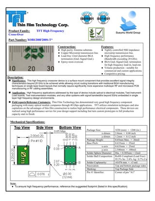
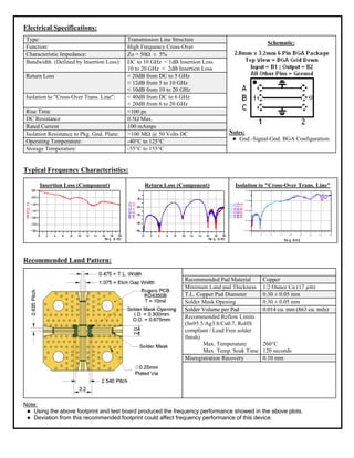
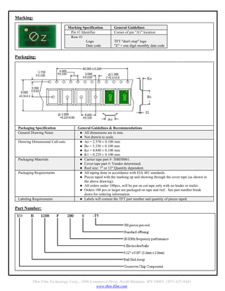
Product Family:            TFT High Frequency
                                                                                                          Susumu World Group
Cross-Over
Part Number: XOB1208F200S-T*

                                                Construction:                                Features:
                                                   High purity Alumina substrate.              Tightly controlled 50Ω impedance
                                                   Copper Microstrip transmission line.        microstrip transmission line.
                                                   Lead-free 12mil diameter BGA                High frequency performance
                                                   termination (Gnd.-Signal-Gnd.).             (Bandwidth exceeding 20 GHz).
                                                   Epoxy-resin overcoat.                       BGA Gnd.-Signal-Gnd. termination
                                                                                               for high frequency lead-in, lead-out.
                                                                                               Volume production - suitable for
                                                                                               commercial and custom applications.
                                                                                               Competitive pricing.
Description:
   Significance: This high frequency crossover device is a surface mount component that provides excellent signal integrity
   characteristics beyond 20 GHz to be achieved while allowing circuit routing transitions with traditional BGA manufacturing
   techniques on single layer board layouts that normally require significantly more expensive multi-layer RF and microwave PCB
   manufacturing or RF cabling assemblies.
   Application: High frequency applications addressed by this type of device include optical to electrical modules, Test Instrument
   Load boards, Test instrumentation modules, and any other systems with signal bandwidths beyond 5GHz embedded in single
   layer high frequency design environments.
   Field reports/Reference Customers: Thin Film Technology has demonstrated very good high frequency component
   packaging with many optical module companies through 40 Gbps applications. TFT utilizes simulation techniques and also
   capitalizes on the advantages of thin film construction to realize high performance electrical components. These devices are
   realized using high performance service for your design support including fast turn custom prototypes to full production
   capacity start to finish.


  Mechanical Specifications:

                                                                             Package Size:            3220 (mm) = 1208 (in.)
                                                                                            x-dimen.  2.0mm = 0.08 inch
                                                                                            y-dimen.  3.2mm = 0.12 inch
                                                                             Package Height:          0.65mm Max. = 26mil
                                                                             Base Pitch:              0.635mm = 25mil
                                                                                            x-axis    0.635mm = 25mil
                                                                                            y-axis    2.540mm = 100mil
                                                                             Solder Sphere Diameter: Dia. = 0.305mm = 12mil
                                                                             Solder Ball Composition: RoHS Compliant (Lead Free)
                                                                                                      95.5% Sn / 3.8% Ag / 0.7% Cu
                                                                             Solder Coplanarity:      ±0.076 mm = ±3 mil
                                                                             Passivation:             Top and bottom package sides
                                                                             Marking:                 Top Package Side
                                                                             Pin #1 Identifier:       Corner of pin "A1"


  Note:
     To ensure high frequency performance, reference the suggested footprint (listed in this specification).
Electrical Specifications:
Type:                                      Transmission Line Structure
                                                                                                 Schematic:
Function:                                  High Frequency Cross-Over
Characteristic Impedance:                  Zo = 50Ω ± 5%
Bandwidth (Defined by Insertion Loss):     DC to 10 GHz < 1dB Insertion Loss
                                           10 to 20 GHz < 2dB Insertion Loss
Return Loss                                < 20dB from DC to 5 GHz
                                           < 12dB from 5 to 10 GHz
                                           < 10dB from 10 to 20 GHz
Isolation to "Cross-Over Trans. Line":     < 40dB from DC to 6 GHz
                                           < 20dB from 6 to 20 GHz
Rise Time                                  <100 ps
DC Resistance                              0.5Ω Max.
Rated Current                              100 mAmps
Isolation Resistance to Pkg. Gnd. Plane:   >100 MΩ @ 50 Volts DC                 Notes:
Operating Temperature:                     -40°C to 125°C                            Gnd.-Signal-Gnd. BGA Configuration.
Storage Temperature:                       -55°C to 155°C


Typical Frequency Characteristics:

      Insertion Loss (Component)                 Return Loss (Component)            Isolation to "Cross-Over Trans. Line"


Recommended Land Pattern:

                                                                 Recommended Pad Material       Copper
                                                                 Minimum Land pad Thickness     1/2 Ounce Cu (17 µm)
                                                                 T.L. Copper Pad Diameter       0.30 ± 0.05 mm
                                                                 Solder Mask Opening            0.30 ± 0.05 mm
                                                                 Solder Volume per Pad          0.014 cu. mm (863 cu. mils)
                                                                 Recommended Reflow Limits
                                                                 (Sn95.5/Ag3.8/Cu0.7, RoHS
                                                                 compliant / Lead Free solder
                                                                 finish)
                                                                         Max. Temperature       260°C
                                                                         Max. Temp. Soak Time   120 seconds
                                                                 Misregistration Recovery       0.10 mm


Note:
   Using the above footprint and test board produced the frequency performance showed in the above plots.
   Deviation from this recommended footprint could affect frequency performance of this device.
Marking:

                                 Marking Specification       General Guidelines
                                  Pin #1 Identifier          Corner of pin "A1" location
                                  Row #1
                                            Logo             TFT "don't stop" logo
                                            Date code        "Z" = one digit monthly date code


Packaging:


 Packaging Specification              General Guidelines & Recommendations
 Genaral Drawing Notes                   All dimensions are in mm.
                                         Not drawin to scale.
 Drawing Dimensional Call-outs           Ao = 2.570 ± 0.100 mm
                                         Bo = 3.330 ± 0.100 mm
                                         Ko = 0.840 ± 0.100 mm
                                         K1 = 0.229 ± 0.100 mm
 Packaging Materials                     Carrier tape part #: 3M058061.
                                         Cover tape part #: Vendor determined.
                                         Reel size: 7" or 13" Quantity dependent.
 Packaging Requirements                  All taping done in accordance with EIA 481 standards.
                                         Pieces taped with the marking up and showing through the cover tape (as shown in
                                         the above drawing).
                                         All orders under 100pcs, will be put on cut tape only with no leader or trailer.
                                         Orders 100 pcs or larger are packaged on tape and reel. See part number break
                                         down for ordering information.
 Labeling Requirements                   Labels will contain the TFT part number and quantity of pieces taped.

Part Number:


         Thin Film Technology Corp., 1980 Commerce Drive, North Mankato, MN 56003, (507) 625-8445
                                             www.thin-film.com

20 Ghz Crossover

  • 1.
    Product Family: TFT High Frequency Susumu World Group Cross-Over Part Number: XOB1208F200S-T* Construction: Features: High purity Alumina substrate. Tightly controlled 50Ω impedance Copper Microstrip transmission line. microstrip transmission line. Lead-free 12mil diameter BGA High frequency performance termination (Gnd.-Signal-Gnd.). (Bandwidth exceeding 20 GHz). Epoxy-resin overcoat. BGA Gnd.-Signal-Gnd. termination for high frequency lead-in, lead-out. Volume production - suitable for commercial and custom applications. Competitive pricing. Description: Significance: This high frequency crossover device is a surface mount component that provides excellent signal integrity characteristics beyond 20 GHz to be achieved while allowing circuit routing transitions with traditional BGA manufacturing techniques on single layer board layouts that normally require significantly more expensive multi-layer RF and microwave PCB manufacturing or RF cabling assemblies. Application: High frequency applications addressed by this type of device include optical to electrical modules, Test Instrument Load boards, Test instrumentation modules, and any other systems with signal bandwidths beyond 5GHz embedded in single layer high frequency design environments. Field reports/Reference Customers: Thin Film Technology has demonstrated very good high frequency component packaging with many optical module companies through 40 Gbps applications. TFT utilizes simulation techniques and also capitalizes on the advantages of thin film construction to realize high performance electrical components. These devices are realized using high performance service for your design support including fast turn custom prototypes to full production capacity start to finish. Mechanical Specifications: Package Size: 3220 (mm) = 1208 (in.) x-dimen. 2.0mm = 0.08 inch y-dimen. 3.2mm = 0.12 inch Package Height: 0.65mm Max. = 26mil Base Pitch: 0.635mm = 25mil x-axis 0.635mm = 25mil y-axis 2.540mm = 100mil Solder Sphere Diameter: Dia. = 0.305mm = 12mil Solder Ball Composition: RoHS Compliant (Lead Free) 95.5% Sn / 3.8% Ag / 0.7% Cu Solder Coplanarity: ±0.076 mm = ±3 mil Passivation: Top and bottom package sides Marking: Top Package Side Pin #1 Identifier: Corner of pin "A1" Note: To ensure high frequency performance, reference the suggested footprint (listed in this specification).
  • 2.
    Electrical Specifications: Type: Transmission Line Structure Schematic: Function: High Frequency Cross-Over Characteristic Impedance: Zo = 50Ω ± 5% Bandwidth (Defined by Insertion Loss): DC to 10 GHz < 1dB Insertion Loss 10 to 20 GHz < 2dB Insertion Loss Return Loss < 20dB from DC to 5 GHz < 12dB from 5 to 10 GHz < 10dB from 10 to 20 GHz Isolation to "Cross-Over Trans. Line": < 40dB from DC to 6 GHz < 20dB from 6 to 20 GHz Rise Time <100 ps DC Resistance 0.5Ω Max. Rated Current 100 mAmps Isolation Resistance to Pkg. Gnd. Plane: >100 MΩ @ 50 Volts DC Notes: Operating Temperature: -40°C to 125°C Gnd.-Signal-Gnd. BGA Configuration. Storage Temperature: -55°C to 155°C Typical Frequency Characteristics: Insertion Loss (Component) Return Loss (Component) Isolation to "Cross-Over Trans. Line" Recommended Land Pattern: Recommended Pad Material Copper Minimum Land pad Thickness 1/2 Ounce Cu (17 µm) T.L. Copper Pad Diameter 0.30 ± 0.05 mm Solder Mask Opening 0.30 ± 0.05 mm Solder Volume per Pad 0.014 cu. mm (863 cu. mils) Recommended Reflow Limits (Sn95.5/Ag3.8/Cu0.7, RoHS compliant / Lead Free solder finish) Max. Temperature 260°C Max. Temp. Soak Time 120 seconds Misregistration Recovery 0.10 mm Note: Using the above footprint and test board produced the frequency performance showed in the above plots. Deviation from this recommended footprint could affect frequency performance of this device.
  • 3.
    Marking: Marking Specification General Guidelines Pin #1 Identifier Corner of pin "A1" location Row #1 Logo TFT "don't stop" logo Date code "Z" = one digit monthly date code Packaging: Packaging Specification General Guidelines & Recommendations Genaral Drawing Notes All dimensions are in mm. Not drawin to scale. Drawing Dimensional Call-outs Ao = 2.570 ± 0.100 mm Bo = 3.330 ± 0.100 mm Ko = 0.840 ± 0.100 mm K1 = 0.229 ± 0.100 mm Packaging Materials Carrier tape part #: 3M058061. Cover tape part #: Vendor determined. Reel size: 7" or 13" Quantity dependent. Packaging Requirements All taping done in accordance with EIA 481 standards. Pieces taped with the marking up and showing through the cover tape (as shown in the above drawing). All orders under 100pcs, will be put on cut tape only with no leader or trailer. Orders 100 pcs or larger are packaged on tape and reel. See part number break down for ordering information. Labeling Requirements Labels will contain the TFT part number and quantity of pieces taped. Part Number: Thin Film Technology Corp., 1980 Commerce Drive, North Mankato, MN 56003, (507) 625-8445 www.thin-film.com