Downloaded 15 times


![6
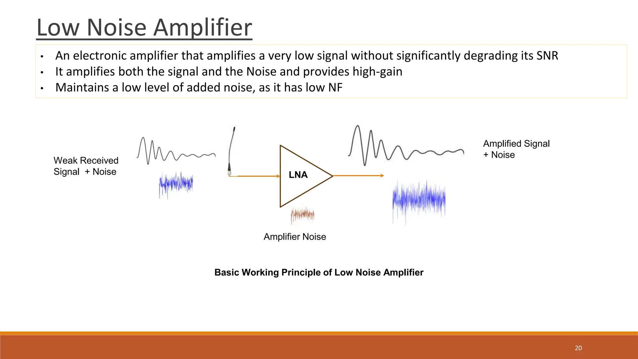
Introduction to TRMs
[Rick Sturdivant & Mike Harris] Compact Ku-Band T/R Module for High-Resolution Radar Imaging of Cold Land Processes
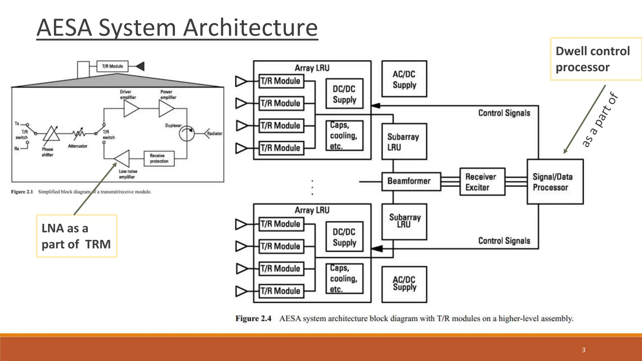
• Transmit/receive modules are the key components in an AESA.
• T/R modules have, at a minimum, four fundamental functions:
• To provide gain and RF power output in transmit mode
• To provide gain and low noise figure in receive mode
• To switch between transmit and receive states
• To provide phase shift for beam steering in the transmit and receive states
• 1K to 10K identical T/R modules may be used in each array face depending on the application.
GPPO Connectors offer RF
performance from DC to 65 GHz.](https://image.slidesharecdn.com/embedded-240403080303-79b01936/75/Transmit-Receive-T-R-Modules-for-Radar-Systems-6-2048.jpg)
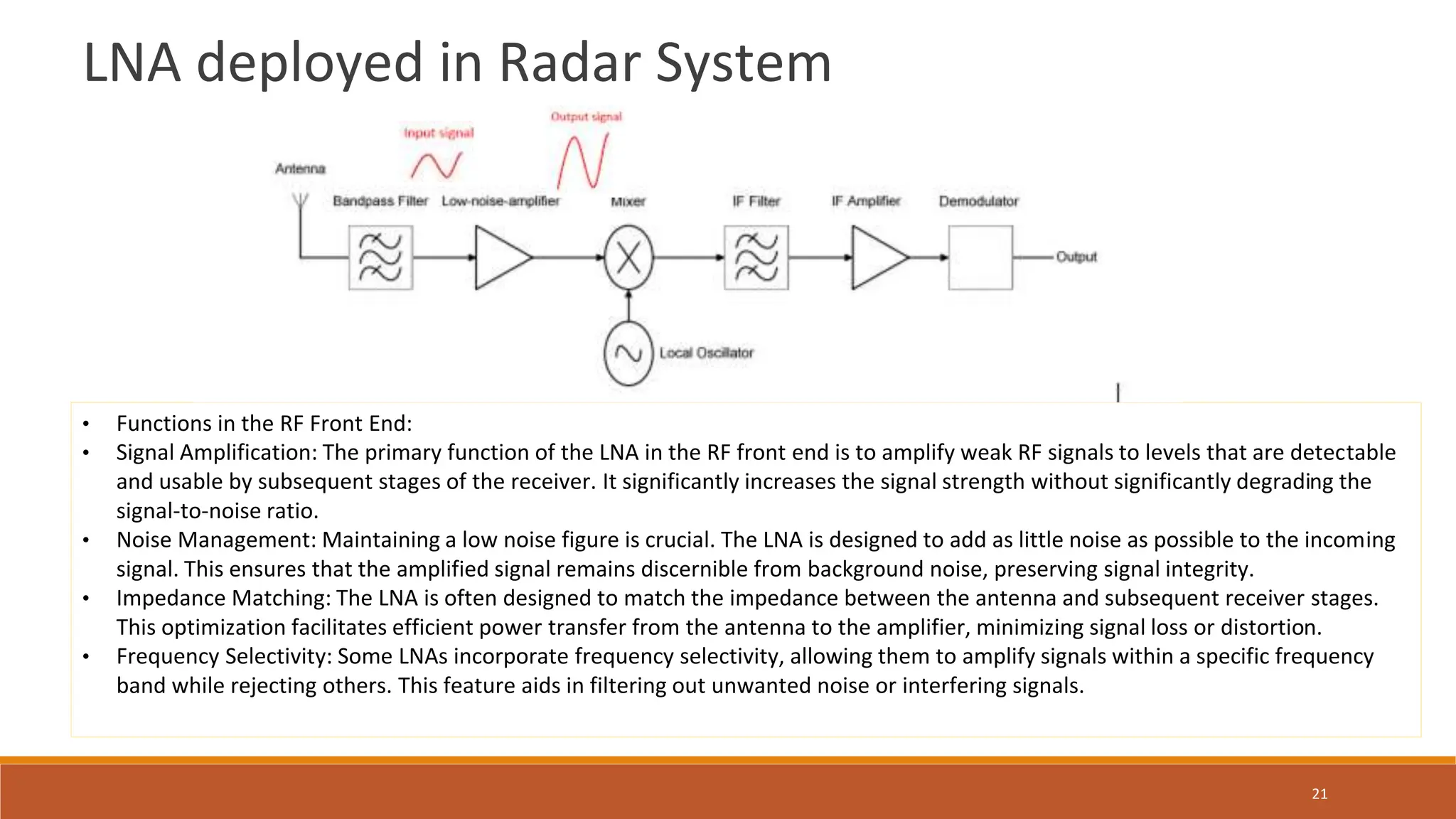
![7
Block diagram of a TRM
[Rick Sturdivant & Mike Harris] Transmit Receive Modules for Radar and Communication Systems
• The attenuator is used in receive mode to tailor the
receive antenna pattern to reduce receive sidelobes.
• A phase shifter circuit controls the electrical insertion
phase of the TR signals, thereby steering the spatially
combined RF energy.
• Driver amplifier and power amplifier perform power
amplification and set the output power level of the
module in the transmit mode.
• A duplexer serves the following purposes:
• Connection: It links the radiating element to both the TR paths.
• Isolation: It ensures isolation between the TR paths, preventing interference.
• Termination: It terminates transmitter power that reflects back into the receive path through the circulator.
• The receive protect circuit limits the input power that reaches the sensitive LNA.
• The low-noise amplifier (LNA) provides low-noise amplification of the radar return signal and is the
principal element that establishes the system noise figure.
• T/R switches are used to switch from transmit to receive mode and are required on the front end of the
module to control signals through the phase shifter and attenuator, as shown in Figure 2.1.](https://image.slidesharecdn.com/embedded-240403080303-79b01936/75/Transmit-Receive-T-R-Modules-for-Radar-Systems-7-2048.jpg)
![8
Performance Requirements of a TRM (Skipping details for now)
[Rick Sturdivant & Mike Harris] Transmit Receive Modules for Radar and Communication Systems
• From Radar system considerations including power-aperture-gain (PAG), allowable array size, weight,
prime power, and cooling, among other considerations we can flow-down the following performance
requirements:
• The number of modules required, Size and weight per module, Power consumption requirements, Peak power
for each module, Efficiency requirements, Noise figure, Phase and amplitude control requirements, and
Module interface requirements.
• As an example, if the peak radiated power is specified as 20 kW and the array has 2,000 elements, each
T/R module will need to deliver 10W, ignoring the radiator losses.](https://image.slidesharecdn.com/embedded-240403080303-79b01936/75/Transmit-Receive-T-R-Modules-for-Radar-Systems-8-2048.jpg)
![9
Early TRM Development Efforts:
[Nicholas 2012] The Development of T/R Modules for Radar Applications
MERA Module:
• The first T/R module was developed on Molecular Electronics for Radar Applications (MERA) program was constructed
using thin film on alumina hybrid integrated circuits with silicon active devices.
• One side of the module contained:
• the transmitter power chain, frequency multiplier, T/R switch, balanced mixer, and IF amplifier,
• while the reverse side contained the
• digital phase shifter, digital control, and LO amplifier.
• The overall power efficiency of the system was low due to the limited microwave performance capability of the silicon
devices.
MMIC-Based Module:
• Integration of microwave circuits on the same substrate known as monolithic microwave integrated circuits (MMICs).
• A typical X-band MMIC-based T/R module from that time period is shown in Figure 2.2.
Mid-1990s MMIC-based X-band T/R module.](https://image.slidesharecdn.com/embedded-240403080303-79b01936/75/Transmit-Receive-T-R-Modules-for-Radar-Systems-9-2048.jpg)
![10
Modern TRMs: Single-Chip T/R Module
[Rick Sturdivant & Mike Harris] Transmit Receive Modules for Radar and Communication Systems
• In this case, the low-noise amplifier (LNA), phase shifter, variable gain amplifier, and high-power amplifier are
designed into in a single GaAs or SiGe integrated circuits.
• Figure 10.1(a) show an example of a single-chip T/R module realized in GaAs.
• Advantages:
• Can achieve lower noise figures for a given process device gate length
• Can generate high output power on transmit
• Disadvantages: cost
• Figure 10.1(b) shows an image of a single-chip T/R module realized in SiGe and
• Figure 10.1 (c) shows a four-channel T/R module realized in SiGe [2].
• Advantages:
• SiGe is that it can have a five to 20 times lower cost than GaAs.
• Another feature of SiGe is that it is low power.](https://image.slidesharecdn.com/embedded-240403080303-79b01936/75/Transmit-Receive-T-R-Modules-for-Radar-Systems-10-2048.jpg)
![11
Modern TRMs: Wafer-Scale Phased Array
[Rick Sturdivant & Mike Harris] Transmit Receive Modules for Radar and Communication Systems
• A team of researchers developed a 64-element wafer-scale phased array [3].
• An image of the array is shown in Figure 10.2.
• This radar uses T/R modules with phase and amplitude control at each element of the array.](https://image.slidesharecdn.com/embedded-240403080303-79b01936/75/Transmit-Receive-T-R-Modules-for-Radar-Systems-11-2048.jpg)
![12
Modern TRMs: The Lowest-Cost Single-Chip T/R
[Rick Sturdivant & Mike Harris] Transmit Receive Modules for Radar and Communication Systems
• SiCMOS having lower cost than SiGe is also been used to realize T/R modules.
• Figure 10.3(a) shows an image of an active quadrature phase shifter realized in Si-CMOS [5, 6].
• This phase shifter can form the heart of a phased array radar since it will achieve the phase shift required to steer the
radar beam.
• Four-element transmit-and-receive chips were developed in 90-nm SiCMOS and are shown in Figure 10.3(b, c).
• The phase shifters in those die are based upon 50-GHz vector modulators.](https://image.slidesharecdn.com/embedded-240403080303-79b01936/75/Transmit-Receive-T-R-Modules-for-Radar-Systems-12-2048.jpg)
![13
Modern TRMs: Digital Beamforming
[Rick Sturdivant & Mike Harris] Transmit Receive Modules for Radar and Communication Systems
• Digital beamforming uses circuitry that is a departure from the normal T/R module [7, 8].
• In the simplest case the T/R module consists of
• front filtering, low-noise amplifier, high-power amplifier, and mixing along with analog-to-digital conversion.
• A simplified block diagram of one element in a digital beamforming array is shown in Figure 10.4.](https://image.slidesharecdn.com/embedded-240403080303-79b01936/75/Transmit-Receive-T-R-Modules-for-Radar-Systems-13-2048.jpg)
![14
Literature Survey (X-Band)
[Rick Sturdivant & Mike Harris] Transmit Receive Modules for Radar and Communication Systems](https://image.slidesharecdn.com/embedded-240403080303-79b01936/75/Transmit-Receive-T-R-Modules-for-Radar-Systems-14-2048.jpg)
![15
Literature Survey (S-Band)
[Rick Sturdivant & Mike Harris] Transmit Receive Modules for Radar and Communication Systems](https://image.slidesharecdn.com/embedded-240403080303-79b01936/75/Transmit-Receive-T-R-Modules-for-Radar-Systems-15-2048.jpg)
![16
Follow up Plan
[Rick Sturdivant & Mike Harris] Transmit Receive Modules for Radar and Communication Systems
● on-the-go: Study & relating characteristics of every TRM component
● Populating list of articles by adding useful/removing unuseful
● Understanding the architectures from the articles and discussing with team](https://image.slidesharecdn.com/embedded-240403080303-79b01936/75/Transmit-Receive-T-R-Modules-for-Radar-Systems-16-2048.jpg)


![22
Performance parameters of LNA
• Low Noise coming from Device (Low NF)
• Linearity (Measurement of third-order Intercept point IP3 and 1dB compression point P1dB)
• High Gain (S21)
• Stability (K factor)
• Matched to antenna or filter (Impedance Matching)
• Low Power Consumption
[Rick Sturdivant & Mike Harris] Transmit Receive Modules for Radar and Communication Systems](https://image.slidesharecdn.com/embedded-240403080303-79b01936/75/Transmit-Receive-T-R-Modules-for-Radar-Systems-22-2048.jpg)


The document is a literature survey on transmit/receive modules (TRMs), commercial off-the-shelf (COTS) low noise amplifiers (LNAs), and dwell control processors, focusing on their design, performance requirements, and recent developments. It includes discussions on early and modern TRM designs, performance parameters of LNAs, and how these components function within radar systems. Additionally, it outlines future plans for research and related studies in the field of electronic systems design for aerospace applications.


![RF Circuit Design - [Ch4-2] LNA, PA, and Broadband Amplifier](https://cdn.slidesharecdn.com/ss_thumbnails/ch4-2-150613064410-lva1-app6891-thumbnail.jpg?width=640&height=640&fit=bounds)


