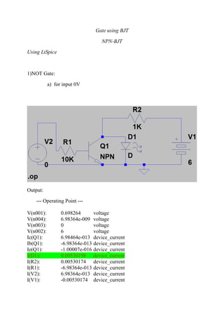
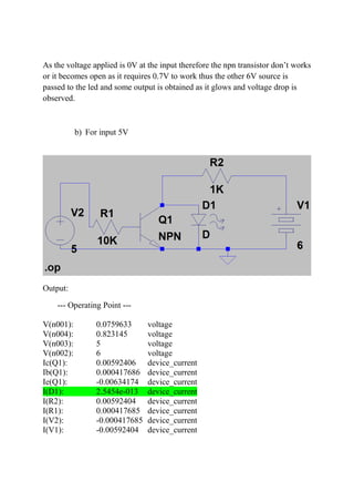
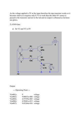
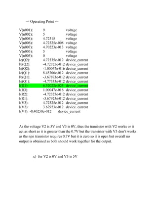
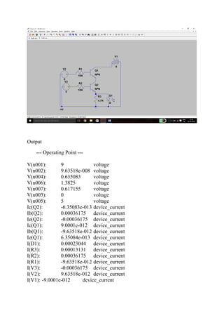
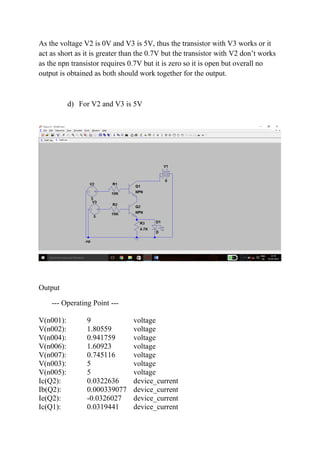
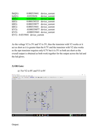
This document summarizes the operation of various logic gates using NPN BJTs in LtSpice. It describes the inputs, outputs and operating points for:
1) A NOT gate with 0V and 5V inputs.
2) An AND gate with various combinations of 0V and 5V inputs.
3) An OR gate with various combinations of 0V and 5V inputs.
4) A NOR gate with 0V and 5V inputs on both transistors.
For each configuration it analyzes whether the transistors are on or off based on the 0.7V threshold, and whether this results in output or not.
Kraus & naimer disconnectors kn pv-gbDien Ha The
Catalog Kraus Naimer, Catalog,
Catalog Thiết Bị Điện Kraus Naimer, Catalog Thiết Bị Điện,
Catalog Biến Tần Kraus Naimer, Catalog Điện Công Nghiệp,
http://dienhathe.com,
Chi tiết các sản phẩm khác của Kraus Naimer tại https://dienhathe.com
Xem thêm các Catalog khác của Kraus Naimer tại https://dienhathe.info
Để nhận báo giá sản phẩm Kraus Naimer vui lòng gọi: 0907.764.966
SPICE MODEL of 1MB08D-120 (Professional+FWDS Model) in SPICE PARKTsuyoshi Horigome
SPICE MODEL of 1MB08D-120 (Professional+FWDS Model) in SPICE PARK. English Version is http://www.spicepark.net. Japanese Version is http://www.spicepark.com by Bee Technologies.
SPICE MODEL of TPCF8102 (Professional+BDP Model) in SPICE PARKTsuyoshi Horigome
SPICE MODEL of TPCF8102 (Professional+BDP Model) in SPICE PARK. English Version is http://www.spicepark.net. Japanese Version is http://www.spicepark.com by Bee Technologies.
The document provides a device modeling report for a Toshiba TA7291P bridge driver IC. It includes:
- Component and part number details
- Circuit simulations and evaluation circuits showing the IC's operation under different input and output conditions
- Simulation results analyzing key parameters like supply current, input characteristics, saturation voltages, and diode characteristics.
The report concludes with 11 sections summarizing the IC's electrical behavior and performance based on circuit simulations, with tables comparing simulated and measured values.
SPICE MODEL of TPC8025 (Standard+BDS Model) in SPICE PARKTsuyoshi Horigome
SPICE MODEL of TPC8025 (Standard+BDS) in SPICE PARK. English Version is http://www.spicepark.net. Japanese Version is http://www.spicepark.com by Bee Technologies.
SPICE MODEL of 1MB08D-120 (Professional+FWDP Model) in SPICE PARKTsuyoshi Horigome
SPICE MODEL of 1MB08D-120 (Professional+FWDP Model) in SPICE PARK. English Version is http://www.spicepark.net. Japanese Version is http://www.spicepark.com by Bee Technologies.
SPICE MODEL of TPCF8302 (Professional+BDP Model) in SPICE PARKTsuyoshi Horigome
SPICE MODEL of TPCF8302 (Professional+BDP Model) in SPICE PARK. English Version is http://www.spicepark.net. Japanese Version is http://www.spicepark.com by Bee Technologies.
SPICE MODEL of TPC8025 (Professional+BDP Model) in SPICE PARKTsuyoshi Horigome
SPICE MODEL of TPC8025 (Professional+BDP Model) in SPICE PARK. English Version is http://www.spicepark.net. Japanese Version is http://www.spicepark.com by Bee Technologies.
The document is a product selection guide from ServoTek Products that includes information about their tachometers, encoders, and transducers. It describes ServoTek as a manufacturer of instrument-grade DC tachometers and encoders for aerospace, automotive, industrial, and other applications. It provides specifications for their various tachometer models, which are grouped by series based on armature length and output voltage. Mounting dimensions and technical specifications are also included to help customers select the appropriate product for their needs.
This document describes the design and simulation of a modified sine wave inverter. The inverter converts 12V DC battery power to 230V AC power for domestic loads up to 500W. It consists of two main circuits: a gate driver circuit and an inverter circuit. The gate driver circuit provides triggering pulses to the inverter circuit. Two methods for the gate driver circuit are presented - one using a 555 timer and CD4017 IC, and another using an Arduino board. Both produce triggering pulses that generate a modified sine wave output from the inverter circuit's transformer. The circuit was simulated in Proteus to verify proper gate pulse generation. The inverter allows powering loads during a power outage using a 12V battery
This document provides instructions for simulating and evaluating the key electrical characteristics of diodes, including:
1. Forward IV characteristic by sweeping the voltage from 0-2V and plotting current from 100mA to 10A
2. Capacitance CV characteristic by applying a 600V pulse and plotting capacitance from 10p to 200pF
3. Reverse recovery characteristic by applying negative and positive voltage pulses and measuring the transition time of the current through a 50Ω resistor from -200mA to 200mA.
The document discusses a simulation of a quasi-resonant switching power supply using an FA5541 controller chip. The simulation results show:
1) The output voltage is regulated at 19V with a maximum current of 5A and an output ripple voltage of approximately 17.5mVP-P.
2) Waveforms of the output responding properly to a step change in load from 3A to 5A.
3) The start-up sequence, showing the controller turning on after the voltage on the VCC pin charges and the auxiliary winding takes over once VCC reaches its threshold.
SPICE MODEL of 1MBH03D-120 (Professional+FWD+SP Model) in SPICE PARKTsuyoshi Horigome
SPICE MODEL of 1MBH03D-120 (Professional+FWD+SP Model) in SPICE PARK. English Version is http://www.spicepark.net. Japanese Version is http://www.spicepark.com by Bee Technologies.
1. The document describes the design of a dynamo-speedometer system that uses the rotational power of a bicycle to determine its speed.
2. The system works by converting the AC voltage output of the dynamo into a regulated DC voltage, then measuring the frequency of the AC signal to determine the rotational speed.
3. The speed is determined either by a digital circuit that counts pulses and displays the speed on 7-segment displays, or by a microcontroller that uses timers to measure frequency and displays the speed on an LCD screen.
This document provides a SPICE model for the SCS110AG silicon carbide Schottky diode manufactured by ROHM. It includes:
- Parameters for the diode model such as saturation current, emission coefficient, and breakdown voltage.
- Simulation results that show good agreement with measurements for forward voltage, junction capacitance, and reverse recovery characteristics.
- Reverse characteristic simulation results that match measurements with less than 3% error.
SCS110AG Professional Model LTspice Model (Free SPICE Model)Tsuyoshi Horigome
This document provides a SPICE model for the SCS110AG silicon carbide Schottky diode manufactured by ROHM. It includes:
- Parameters for the diode model such as saturation current, emission coefficient, and breakdown voltage.
- Simulation results that show good agreement with measurements for forward voltage, junction capacitance, and reverse recovery characteristics.
- Reverse characteristic simulation results that match measurements with less than 3% error.
SPICE MODEL of 1MBH03D-120 (Professional+FWDP Model) in SPICE PARKTsuyoshi Horigome
SPICE MODEL of 1MBH03D-120 (Professional+FWDP Model) in SPICE PARK. English Version is http://www.spicepark.net. Japanese Version is http://www.spicepark.com by Bee Technologies.
ppt of automatic room light controller and BI directional counterMannavapremkumar
This document is a project presentation for an automatic room light controller. It includes the objective, introduction, block diagram, circuit diagram, advantages, disadvantages, limitations and applications. The block diagram shows the components used including IR transmitters and receivers, timers, counters and a relay to control the room light. The circuit diagram provides more details of the electronic components and connections used to automatically turn the light on when motion is detected and off when the room is empty.
SPICE MODEL of CM600HU-12H (Professional+FWDP Model) in SPICE PARKTsuyoshi Horigome
SPICE MODEL of CM600HU-12H (Professional+FWDP Model) in SPICE PARK. English Version is http://www.spicepark.net. Japanese Version is http://www.spicepark.com by Bee Technologies.
SPICE MODEL of 1MBH03D-120 (Professional+FWDS Model) in SPICE PARKTsuyoshi Horigome
SPICE MODEL of 1MBH03D-120 (Professional+FWDS Model) in SPICE PARK. English Version is http://www.spicepark.net. Japanese Version is http://www.spicepark.com by Bee Technologies.
This document contains a SPICE model for the Cree CSD10060G silicon carbide schottky diode, including:
- The SPICE subcircuit definition for the diode model.
- Descriptions of the model parameters.
- Simulation results for forward and reverse I-V characteristics and junction capacitance, along with comparisons to measurements.
The document describes various types of clipping circuits used for non-linear wave shaping. It discusses positive clipping, negative clipping, and slicing circuits. Positive clipping circuits clip the positive portions of a signal that exceed a reference voltage. Negative clipping circuits clip the negative portions above a reference level. A slicing circuit clips both positive and negative portions. The document provides circuit diagrams and expected input and output waveforms for each type of clipping circuit using a diode and resistor. It aims to study these clipping circuits experimentally and verify the theoretical responses.
Reimagining Your Library Space: How to Increase the Vibes in Your Library No ...Diana Rendina
Librarians are leading the way in creating future-ready citizens – now we need to update our spaces to match. In this session, attendees will get inspiration for transforming their library spaces. You’ll learn how to survey students and patrons, create a focus group, and use design thinking to brainstorm ideas for your space. We’ll discuss budget friendly ways to change your space as well as how to find funding. No matter where you’re at, you’ll find ideas for reimagining your space in this session.
हिंदी वर्णमाला पीपीटी, hindi alphabet PPT presentation, hindi varnamala PPT, Hindi Varnamala pdf, हिंदी स्वर, हिंदी व्यंजन, sikhiye hindi varnmala, dr. mulla adam ali, hindi language and literature, hindi alphabet with drawing, hindi alphabet pdf, hindi varnamala for childrens, hindi language, hindi varnamala practice for kids, https://www.drmullaadamali.com
How to Build a Module in Odoo 17 Using the Scaffold MethodCeline George
Odoo provides an option for creating a module by using a single line command. By using this command the user can make a whole structure of a module. It is very easy for a beginner to make a module. There is no need to make each file manually. This slide will show how to create a module using the scaffold method.
ISO/IEC 27001, ISO/IEC 42001, and GDPR: Best Practices for Implementation and...PECB
Denis is a dynamic and results-driven Chief Information Officer (CIO) with a distinguished career spanning information systems analysis and technical project management. With a proven track record of spearheading the design and delivery of cutting-edge Information Management solutions, he has consistently elevated business operations, streamlined reporting functions, and maximized process efficiency.
Certified as an ISO/IEC 27001: Information Security Management Systems (ISMS) Lead Implementer, Data Protection Officer, and Cyber Risks Analyst, Denis brings a heightened focus on data security, privacy, and cyber resilience to every endeavor.
His expertise extends across a diverse spectrum of reporting, database, and web development applications, underpinned by an exceptional grasp of data storage and virtualization technologies. His proficiency in application testing, database administration, and data cleansing ensures seamless execution of complex projects.
What sets Denis apart is his comprehensive understanding of Business and Systems Analysis technologies, honed through involvement in all phases of the Software Development Lifecycle (SDLC). From meticulous requirements gathering to precise analysis, innovative design, rigorous development, thorough testing, and successful implementation, he has consistently delivered exceptional results.
Throughout his career, he has taken on multifaceted roles, from leading technical project management teams to owning solutions that drive operational excellence. His conscientious and proactive approach is unwavering, whether he is working independently or collaboratively within a team. His ability to connect with colleagues on a personal level underscores his commitment to fostering a harmonious and productive workplace environment.
Date: May 29, 2024
Tags: Information Security, ISO/IEC 27001, ISO/IEC 42001, Artificial Intelligence, GDPR
-------------------------------------------------------------------------------
Find out more about ISO training and certification services
Training: ISO/IEC 27001 Information Security Management System - EN | PECB
ISO/IEC 42001 Artificial Intelligence Management System - EN | PECB
General Data Protection Regulation (GDPR) - Training Courses - EN | PECB
Webinars: https://pecb.com/webinars
Article: https://pecb.com/article
-------------------------------------------------------------------------------
For more information about PECB:
Website: https://pecb.com/
LinkedIn: https://www.linkedin.com/company/pecb/
Facebook: https://www.facebook.com/PECBInternational/
Slideshare: http://www.slideshare.net/PECBCERTIFICATION
Main Java[All of the Base Concepts}.docxadhitya5119
This is part 1 of my Java Learning Journey. This Contains Custom methods, classes, constructors, packages, multithreading , try- catch block, finally block and more.
This presentation was provided by Steph Pollock of The American Psychological Association’s Journals Program, and Damita Snow, of The American Society of Civil Engineers (ASCE), for the initial session of NISO's 2024 Training Series "DEIA in the Scholarly Landscape." Session One: 'Setting Expectations: a DEIA Primer,' was held June 6, 2024.
A workshop hosted by the South African Journal of Science aimed at postgraduate students and early career researchers with little or no experience in writing and publishing journal articles.
বাংলাদেশের অর্থনৈতিক সমীক্ষা ২০২৪ [Bangladesh Economic Review 2024 Bangla.pdf] কম্পিউটার , ট্যাব ও স্মার্ট ফোন ভার্সন সহ সম্পূর্ণ বাংলা ই-বুক বা pdf বই " সুচিপত্র ...বুকমার্ক মেনু 🔖 ও হাইপার লিংক মেনু 📝👆 যুক্ত ..
আমাদের সবার জন্য খুব খুব গুরুত্বপূর্ণ একটি বই ..বিসিএস, ব্যাংক, ইউনিভার্সিটি ভর্তি ও যে কোন প্রতিযোগিতা মূলক পরীক্ষার জন্য এর খুব ইম্পরট্যান্ট একটি বিষয় ...তাছাড়া বাংলাদেশের সাম্প্রতিক যে কোন ডাটা বা তথ্য এই বইতে পাবেন ...
তাই একজন নাগরিক হিসাবে এই তথ্য গুলো আপনার জানা প্রয়োজন ...।
বিসিএস ও ব্যাংক এর লিখিত পরীক্ষা ...+এছাড়া মাধ্যমিক ও উচ্চমাধ্যমিকের স্টুডেন্টদের জন্য অনেক কাজে আসবে ...
Film vocab for eal 3 students: Australia the movie
Transistor as a Gates
1. Gate using BJT
NPN-BJT
Using LtSpice
1)NOT Gate:
a) for input 0V
Output:
--- Operating Point ---
V(n001): 0.698264 voltage
V(n004): 6.98364e-009 voltage
V(n003): 0 voltage
V(n002): 6 voltage
Ic(Q1): 6.98464e-013 device_current
Ib(Q1): -6.98364e-013 device_current
Ie(Q1): -1.00007e-016 device_current
I(D1): 0.00530198 device_current
I(R2): 0.00530174 device_current
I(R1): -6.98364e-013 device_current
I(V2): 6.98364e-013 device_current
I(V1): -0.00530174 device_current
2. As the voltage applied is 0V at the input therefore the npn transistor don’t works
or it becomes open as it requires 0.7V to work thus the other 6V source is
passed to the led and some output is obtained as it glows and voltage drop is
observed.
b) For input 5V
Output:
--- Operating Point ---
V(n001): 0.0759633 voltage
V(n004): 0.823145 voltage
V(n003): 5 voltage
V(n002): 6 voltage
Ic(Q1): 0.00592406 device_current
Ib(Q1): 0.000417686 device_current
Ie(Q1): -0.00634174 device_current
I(D1): 2.5454e-013 device_current
I(R2): 0.00592404 device_current
I(R1): 0.000417685 device_current
I(V2): -0.000417685 device_current
I(V1): -0.00592404 device_current
3. As the voltage applied is 5V at the input therefore the npn transistor works or it
becomes short as it requires only 0.7V to work thus the other 6V source is
passed to the transistor and not to the led and no output is obtained as led does
not glows.
2) AND Gate:
a) for V2 and V3 is 0V
Output
--- Operating Point ---
V(n001): 9 voltage
V(n002): 9.00015e-008 voltage
V(n004): 4.97559e-005 voltage
V(n006): 4.99481e-013 voltage
V(n007): 9.03264e-016 voltage
4. V(n003): 0 voltage
V(n005): 0 voltage
Ic(Q2): 5.01403e-017 device_current
Ib(Q2): -4.99481e-017 device_current
Ie(Q2): -1.92184e-019 device_current
Ic(Q1): 9.0002e-012 device_current
Ib(Q1): -9.00015e-012 device_current
Ie(Q1): -5.01403e-017 device_current
I(D1): 1.25187e-027 device_current
I(R3): 1.92184e-019 device_current
I(R2): -4.99481e-017 device_current
I(R1): -9.00015e-012 device_current
I(V3): 4.99481e-017 device_current
I(V2): 9.00015e-012 device_current
I(V1): -9.0002e-012 device_current
As the voltage V2 and V3 is 0V, thus the both transistor don’t work as the npn
transistor requires 0.7V, so no output is obtained.
b) for V2 is 5V and V3 is 0V
Output
5. --- Operating Point ---
V(n001): 9 voltage
V(n002): 5 voltage
V(n004): 4.72315 voltage
V(n006): 4.72325e-008 voltage
V(n007): 4.70223e-013 voltage
V(n003): 5 voltage
V(n005): 0 voltage
Ic(Q2): 4.72335e-012 device_current
Ib(Q2): -4.72325e-012 device_current
Ie(Q2): -1.00047e-016 device_current
Ic(Q1): 8.45206e-012 device_current
Ib(Q1): -3.67873e-012 device_current
Ie(Q1): -4.77333e-012 device_current
I(D1): 6.52022e-025 device_current
I(R3): 1.00047e-016 device_current
I(R2): -4.72325e-012 device_current
I(R1): -3.67923e-012 device_current
I(V3): 4.72325e-012 device_current
I(V2): 3.67923e-012 device_current
I(V1): -8.40258e-012 device_current
As the voltage V2 is 5V and V3 is 0V, thus the transistor with V2 works or it
act as short as it is greater than the 0.7V but the transistor with V3 don’t works
as the npn transistor requires 0.7V but it is zero so it is open but overall no
output is obtained as both should work together for the output.
c) for V2 is 0V and V3 is 5V
6. Output
--- Operating Point ---
V(n001): 9 voltage
V(n002): 9.63518e-008 voltage
V(n004): 0.635083 voltage
V(n006): 1.3825 voltage
V(n007): 0.617155 voltage
V(n003): 0 voltage
V(n005): 5 voltage
Ic(Q2): -6.35083e-013 device_current
Ib(Q2): 0.00036175 device_current
Ie(Q2): -0.00036175 device_current
Ic(Q1): 9.0001e-012 device_current
Ib(Q1): -9.63518e-012 device_current
Ie(Q1): 6.35084e-013 device_current
I(D1): 0.00023044 device_current
I(R3): 0.00013131 device_current
I(R2): 0.00036175 device_current
I(R1): -9.63518e-012 device_current
I(V3): -0.00036175 device_current
I(V2): 9.63518e-012 device_current
I(V1): -9.0001e-012 device_current
7. As the voltage V2 is 0V and V3 is 5V, thus the transistor with V3 works or it
act as short as it is greater than the 0.7V but the transistor with V2 don’t works
as the npn transistor requires 0.7V but it is zero so it is open but overall no
output is obtained as both should work together for the output.
d) For V2 and V3 is 5V
Output
--- Operating Point ---
V(n001): 9 voltage
V(n002): 1.80559 voltage
V(n004): 0.941759 voltage
V(n006): 1.60923 voltage
V(n007): 0.745116 voltage
V(n003): 5 voltage
V(n005): 5 voltage
Ic(Q2): 0.0322636 device_current
Ib(Q2): 0.000339077 device_current
Ie(Q2): -0.0326027 device_current
Ic(Q1): 0.0319441 device_current
8. Ib(Q1): 0.000319441 device_current
Ie(Q1): -0.0322636 device_current
I(D1): 0.0324441 device_current
I(R3): 0.000158535 device_current
I(R2): 0.000339077 device_current
I(R1): 0.000319441 device_current
I(V3): -0.000339077 device_current
I(V2): -0.000319441 device_current
I(V1): -0.0319441 device_current
As the voltage V2 is 5V and V3 is 5V, thus the transistor with V3 works or it
act as short as it is greater than the 0.7V and the transistor with V2 also works
as the npn transistor requires only 0.7V but it is 5V so both are short so the
overall output is obtained as both work together for the output across the led and
the led glows.
3) OR Gate:
a) For V2 is 0V and V3 is 0V
Output:
9. --- Operating Point ---
V(n001): 9 voltage
V(n002): 9.0001e-008 voltage
V(n004): 9.40849e-013 voltage
V(n007): 9.0001e-008 voltage
V(n003): 0 voltage
V(n006): 0 voltage
Ic(Q2): 9.0002e-012 device_current
Ib(Q2): -9.0001e-012 device_current
Ie(Q2): -1.0009e-016 device_current
Ic(Q1): 9.0002e-012 device_current
Ib(Q1): -9.0001e-012 device_current
Ie(Q1): -1.0009e-016 device_current
I(D1): 1.3046e-024 device_current
I(R3): 2.00181e-016 device_current
I(R2): -9.0001e-012 device_current
I(R1): -9.0001e-012 device_current
I(V3): 9.0001e-012 device_current
I(V2): 9.0001e-012 device_current
I(V1): -1.80004e-011 device_current
As the V2 and V3 is 0V so the both transistor does not works as they requires
only 0.7V in the npn transistors so both act as the open and the 9V source is not
passed on to these and at last the current can’t reaches the led diode and does
not glow and output is not obtained.
b) For V2 is 5V and V3 is 0V
10. Output:
--- Operating Point ---
V(n001): 9 voltage
V(n002): 1.61173 voltage
V(n004): 0.746377 voltage
V(n007): 9.74648e-008 voltage
V(n003): 5 voltage
V(n006): 0 voltage
Ic(Q2): 9.0001e-012 device_current
Ib(Q2): -9.74648e-012 device_current
Ie(Q2): 7.46378e-013 device_current
Ic(Q1): 0.0338827 device_current
Ib(Q1): 0.000338827 device_current
Ie(Q1): -0.0342216 device_current
I(D1): 0.0340641 device_current
I(R3): 0.000158804 device_current
I(R2): -9.74648e-012 device_current
I(R1): 0.000338827 device_current
I(V3): 9.74648e-012 device_current
I(V2): -0.000338827 device_current
I(V1): -0.0338827 device_current
As the V3 is 0V and V2 is 5V so the transistor with V3 does not works as it
requires only 0.7V in the npn transistors so it act as the open and the transistor
with V2 works as it is greater than 0.7V and got short so the 9V source is passed
11. on to the one of transistor and at last the current reaches the led diode and it
glow and output is obtained.
c) for V2 is 0V and V3 is 5V
Output:
--- Operating Point ---
V(n001): 9 voltage
V(n002): 9.74648e-008 voltage
V(n004): 0.746377 voltage
V(n007): 1.61173 voltage
V(n003): 0 voltage
V(n006): 5 voltage
Ic(Q2): 0.0338827 device_current
Ib(Q2): 0.000338827 device_current
Ie(Q2): -0.0342216 device_current
Ic(Q1): 9.0001e-012 device_current
Ib(Q1): -9.74648e-012 device_current
Ie(Q1): 7.46378e-013 device_current
12. I(D1): 0.0340641 device_current
I(R3): 0.000158804 device_current
I(R2): 0.000338827 device_current
I(R1): -9.74648e-012 device_current
I(V3): -0.000338827 device_current
I(V2): 9.74648e-012 device_current
I(V1): -0.0338827 device_current
As the V2 is 0V and V3 is 5V so the transistor with V2 does not works as it
requires only 0.7V in the npn transistors so it act as the open and the transistor
with V3 works as it is greater than 0.7V and got short so the 9V source is
passed on to the one of transistor and at last the current reaches the led diode
and it glow and output is obtained.
d) For V2 and V3 is 5V
Output:
--- Operating Point ---
V(n001): 9 voltage
V(n002): 1.62944 voltage
V(n004): 0.764227 voltage
V(n007): 1.62944 voltage
V(n003): 5 voltage
V(n006): 5 voltage
13. Ic(Q2): 0.0337056 device_current
Ib(Q2): 0.000337056 device_current
Ie(Q2): -0.0340426 device_current
Ic(Q1): 0.0337056 device_current
Ib(Q1): 0.000337056 device_current
Ie(Q1): -0.0340426 device_current
I(D1): 0.0679227 device_current
I(R3): 0.000162601 device_current
I(R2): 0.000337056 device_current
I(R1): 0.000337056 device_current
I(V3): -0.000337056 device_current
I(V2): -0.000337056 device_current
I(V1): -0.0674112 device_current
As the both the input is 5V so the both transistor works as they requires only
0.7V in the npn transistors so both act as the short and the 9V source is passed
on to these and at last the current reaches the led diode and makes it glow and
output is obtained.
4) NOR Gate
a) For V2 and V3 is 0V
14. Output
--- Operating Point ---
V(n001): 0.698262 voltage
V(n003): 6.98362e-009 voltage
V(n007): 6.98362e-009 voltage
V(n004): 0 voltage
V(n006): 0 voltage
V(n002): 6 voltage
Ic(Q2): 6.98462e-013 device_current
Ib(Q2): -6.98362e-013 device_current
Ie(Q2): -1.00007e-016 device_current
Ic(Q1): 6.98462e-013 device_current
Ib(Q1): -6.98362e-013 device_current
Ie(Q1): -1.00007e-016 device_current
I(D1): 0.00530174 device_current
I(R3): -0.00530174 device_current
I(R2): -6.98362e-013 device_current
I(R1): -6.98362e-013 device_current
I(V1): -0.00530174 device_current
I(V3): 6.98362e-013 device_current
I(V2): 6.98362e-013 device_current
15. As the V2 and V3 is 0V so the both transistor does not works as they requires
only 0.7V in the npn transistors so both act as the open and the 9V source is not
passed on to these and passed from the led and it glows and output is obtained.
b) For V2 is 0V and V3 is 5V
Output:
--- Operating Point ---
V(n001): 0.0759632 voltage
V(n003): 7.60579e-010 voltage
V(n007): 0.823145 voltage
V(n004): 0 voltage
V(n006): 5 voltage
V(n002): 6 voltage
Ic(Q2): 0.00592404 device_current
Ib(Q2): 0.000417685 device_current
Ie(Q2): -0.00634172 device_current
Ic(Q1): 7.61526e-014 device_current
Ib(Q1): -7.60579e-014 device_current
Ie(Q1): -9.46979e-017 device_current
16. I(D1): 2.54539e-013 device_current
I(R3): -0.00592404 device_current
I(R2): 0.000417685 device_current
I(R1): -7.60579e-014 device_current
I(V1): -0.00592404 device_current
I(V3): -0.000417685 device_current
I(V2): 7.60579e-014 device_current
As the V2 is 0V and V3 is 5V so the transistor with V2 does not works as it
requires only 0.7V in the npn transistors so it act as the open and the transistor
with V3 works as it is greater than 0.7V and got short so the current can’t pass
through the transistors across V2 but pass through the transistor across V3, so
the current pass to this short transistor and can’t pass to the Led thus the led
does not glows and output is zero.
c) V2 is 5v and V3 is 0V
Output
--- Operating Point ---
V(n001): 0.0759632 voltage
V(n003): 0.823145 voltage
V(n007): 7.60579e-010 voltage
V(n004): 5 voltage
V(n006): 0 voltage
17. V(n002): 6 voltage
Ic(Q2): 7.61526e-014 device_current
Ib(Q2): -7.60579e-014 device_current
Ie(Q2): -9.46979e-017 device_current
Ic(Q1): 0.00592404 device_current
Ib(Q1): 0.000417685 device_current
Ie(Q1): -0.00634172 device_current
I(D1): 2.54539e-013 device_current
I(R3): -0.00592404 device_current
I(R2): -7.60579e-014 device_current
I(R1): 0.000417685 device_current
I(V1): -0.00592404 device_current
I(V3): 7.60579e-014 device_current
I(V2): -0.000417685 device_current
As the V3 is 0V and V2 is 5V so the transistor with V3 does not works as it
requires only 0.7V in the npn transistors so it act as the open and the transistor
with V2 works as it is greater than 0.7V and got short so the current can’t pass
through the transistors across V3 but pass through the transistor across V2 , so
the current pass to this short transistor and can’t pass to the Led thus the led
does not glows and output is zero
d) For V2 and V3 is 5V
18. Output
--- Operating Point ---
V(n001): 0.0589801 voltage
V(n003): 0.808309 voltage
V(n007): 0.808309 voltage
V(n004): 5 voltage
V(n006): 5 voltage
V(n002): 6 voltage
Ic(Q2): 0.00297051 device_current
Ib(Q2): 0.000419169 device_current
Ie(Q2): -0.00338968 device_current
Ic(Q1): 0.00297051 device_current
Ib(Q1): 0.000419169 device_current
Ie(Q1): -0.00338968 device_current
I(D1): 1.46777e-013 device_current
I(R3): -0.00594102 device_current
I(R2): 0.000419169 device_current
I(R1): 0.000419169 device_current
I(V1): -0.00594102 device_current
I(V3): -0.000419169 device_current
I(V2): -0.000419169 device_current
As the V2 is 5V and V3 is 5V so the transistor with V2 does works as it requires
only 0.7V in the npn transistors so it act as the short and the transistor with V3
19. also works as it is greater than 0.7V and got short so the current pass through
the transistors across V2 and V3 both and can’t pass to the Led thus the led does
not glows and output is zero.
5) NAND Gate
a) For V2 and V3 is 0V
Output
--- Operating Point ---
V(n001): 0.698262 voltage
V(n003): 6.98412e-009 voltage
V(n005): 4.97145e-005 voltage
V(n007): 4.99065e-013 voltage
V(n004): 0 voltage
V(n006): 0 voltage
V(n002): 6 voltage
Ic(Q2): 5.00986e-017 device_current
Ib(Q2): -4.99065e-017 device_current
20. Ie(Q2): -1.92024e-019 device_current
Ic(Q1): 6.98462e-013 device_current
Ib(Q1): -6.98412e-013 device_current
Ie(Q1): -5.00986e-017 device_current
I(D1): 0.00530174 device_current
I(R3): -0.00530174 device_current
I(R2): -4.99065e-017 device_current
I(R1): -6.98412e-013 device_current
I(V1): -0.00530174 device_current
I(V3): 4.99065e-017 device_current
I(V2): 6.98412e-013 device_current
As the voltage V2 and V3 is 0V, thus the both transistor don’t work as the npn
transistor requires 0.7V, so becomes open and the whole current pass through
the led and it glows and the output is obtained
b) For V2 is 5V and V3 is 0V
Output:
--- Operating Point ---
V(n001): 0.699932 voltage
V(n003): 1.44714 voltage
V(n005): 0.70019 voltage
21. V(n007): 7.00289e-009 voltage
V(n004): 5 voltage
V(n006): 0 voltage
V(n002): 6 voltage
Ic(Q2): 7.0039e-013 device_current
Ib(Q2): -7.00289e-013 device_current
Ie(Q2): -1.00007e-016 device_current
Ic(Q1): -0.000355281 device_current
Ib(Q1): 0.000355286 device_current
Ie(Q1): -4.72982e-009 device_current
I(D1): 0.00565535 device_current
I(R3): -0.00530007 device_current
I(R2): -7.00289e-013 device_current
I(R1): 0.000355286 device_current
I(V1): -0.00530007 device_current
I(V3): 7.00289e-013 device_current
I(V2): -0.000355286 device_current
As the voltage V2 is 5V and V3 is 0V, thus the transistor with V2 works or it
act as short as it is greater than the 0.7V but the transistor with V3 don’t works
as the npn transistor requires 0.7V but it is zero so it is open but overall this
does not work as it is open so the whole current is passed to the led and it glows
and output is obtained.
c) For V2 is 0V and V3 is 5V
22. Output:
--- Operating Point ---
V(n001): 0.698262 voltage
V(n003): 7.16291e-009 voltage
V(n005): 0.0179282 voltage
V(n007): 0.769397 voltage
V(n004): 0 voltage
V(n006): 5 voltage
V(n002): 6 voltage
Ic(Q2): -1.78777e-014 device_current
Ib(Q2): 0.00042306 device_current
Ie(Q2): -0.00042306 device_current
Ic(Q1): 6.98412e-013 device_current
Ib(Q1): -7.16291e-013 device_current
Ie(Q1): 1.78787e-014 device_current
I(D1): 0.00530174 device_current
I(R3): -0.00530174 device_current
I(R2): 0.00042306 device_current
I(R1): -7.16291e-013 device_current
I(V1): -0.00530174 device_current
I(V3): -0.00042306 device_current
I(V2): 7.16291e-013 device_current
23. As the voltage V2 is 0V and V3 is 5V, thus the transistor with V3 works or it
act as short as it is greater than the 0.7V but the transistor with V2 don’t works
as the npn transistor requires 0.7V but this circuit does not work as it is open
and the whole current pass to the led and it glows and output is obtained.
d) For V2 and V3 is 5V
Output
--- Operating Point ---
V(n001): 0.153564 voltage
V(n003): 0.900241 voltage
V(n005): 0.0774538 voltage
V(n007): 0.824386 voltage
V(n004): 5 voltage
V(n006): 5 voltage
V(n002): 6 voltage
Ic(Q2): 0.00625641 device_current
Ib(Q2): 0.000417561 device_current
Ie(Q2): -0.00667397 device_current
Ic(Q1): 0.00584644 device_current
Ib(Q1): 0.000409976 device_current
Ie(Q1): -0.00625641 device_current
24. I(D1): 3.93205e-012 device_current
I(R3): -0.00584644 device_current
I(R2): 0.000417561 device_current
I(R1): 0.000409976 device_current
I(V1): -0.00584644 device_current
I(V3): -0.000417561 device_current
I(V2): -0.000409976 device_current
As the voltage V2 and V3 is 5V, thus the both transistor works as the npn
transistor requires 0.7V, and got shorted, thus the current pass through it and not
to the led so no output is obtained as led does not glows.
By
Lijin G Varghese