Download to read offline
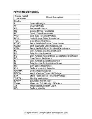
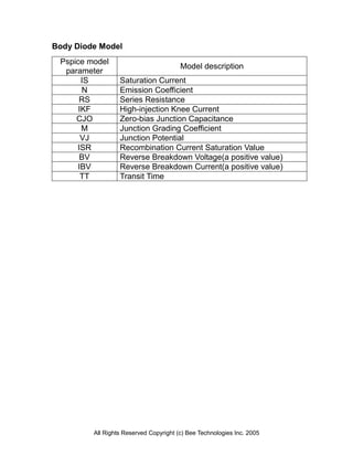
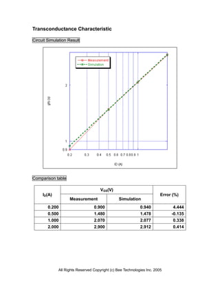
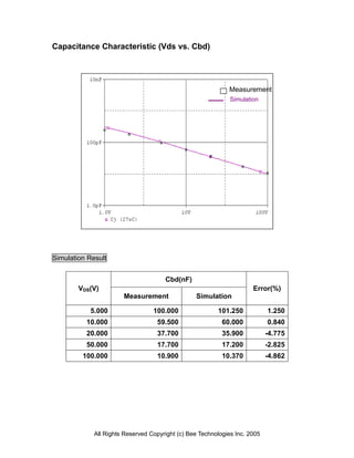
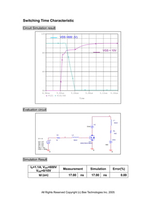
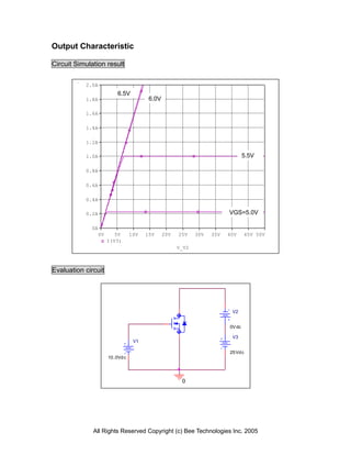
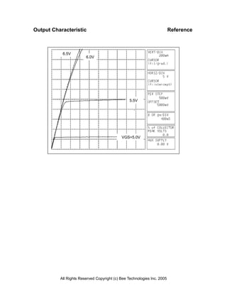
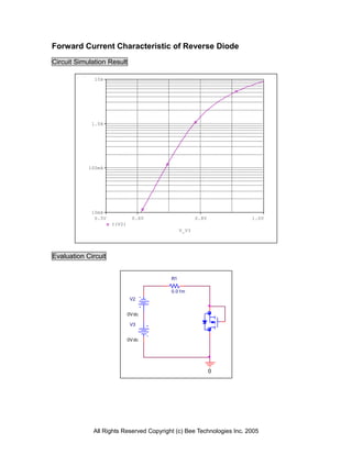
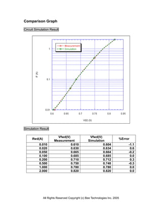
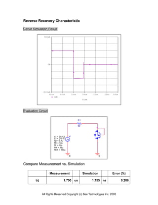
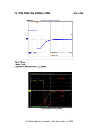

The document provides a detailed device modeling report for a power MOSFET (2SK3728-01MR) from Fuji Electric Co., Ltd., including parameters such as transconductance, gate capacitance, and characteristics of both the power MOSFET and its body diode. It contains simulation results comparing measurements, error percentages, and circuit specifications related to various behaviors of the device under different conditions. The report also includes performance metrics for characteristics like switching time, output, and reverse recovery, with diagrams and tables summarizing the findings.


