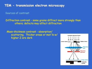
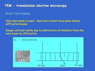
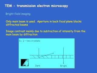
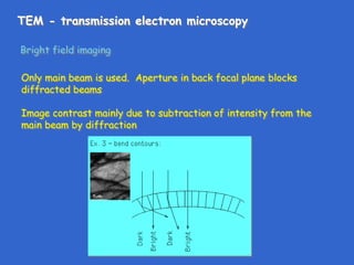
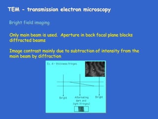
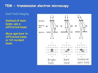
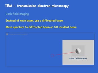
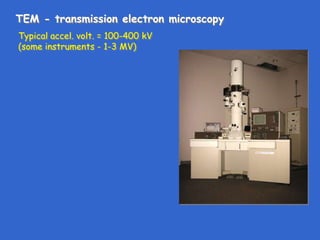
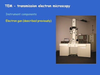
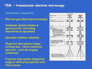
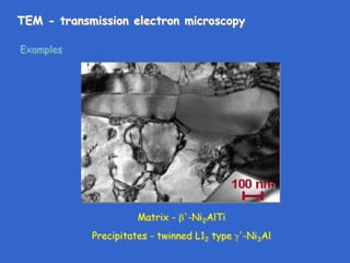
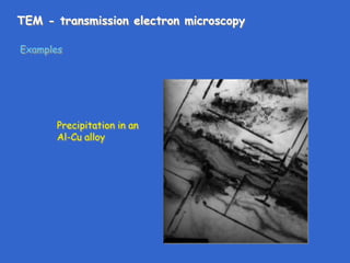
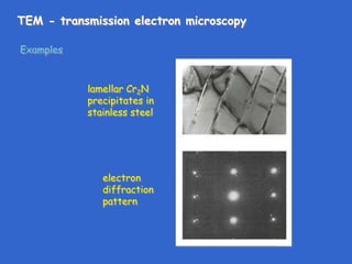
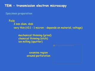
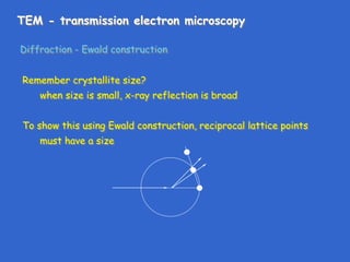
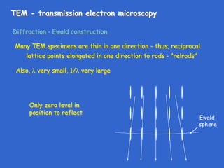
Transmission electron microscopy (TEM) uses electrons instead of light to image materials at the nanoscale. Key components of a TEM include an electron gun, condenser lenses, a specimen holder, an objective lens that forms the image, and projector lenses that magnify the image. TEMs can form images of a specimen's internal structure or collect diffraction patterns from which the specimen's crystal structure can be determined. Specimen preparation often involves thinning to less than 100 nm thickness. TEM provides several contrast mechanisms and imaging modes for revealing details about a material's microstructure, defects, and composition.

![TEM - transmission electron microscopy
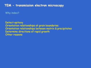
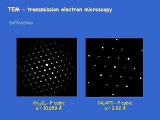
Diffraction
Symmetry of diffraction pattern reflects
symmetry of crystal around beam direction
Why does 3-fold diffraction pattern look hexagonal?
[111] in cubic [001] in hexagonal
Example:
6-fold in hexagonal, 3-fold in cubic](https://image.slidesharecdn.com/tem-240220124846-86f052b5/85/TEM-transmission-electron-microscopy-in-depth-14-320.jpg)
![TEM - transmission electron microscopy
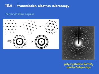
Diffraction
Note: all diffraction
patterns are
centrosymmetric,
even if crystal structure
is not centrosymmetric
(Friedel's law)
Some 0-level patterns
thus exhibit higher
rotational symmetry than
structure has
P cubic reciprocal lattice
layers along [111] direction
0-level
l = +1 level
l = -1 level](https://image.slidesharecdn.com/tem-240220124846-86f052b5/85/TEM-transmission-electron-microscopy-in-depth-15-320.jpg)
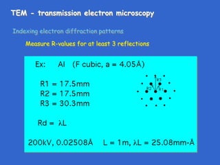
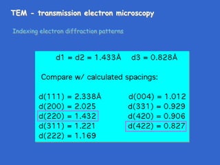
![TEM - transmission electron microscopy
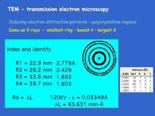
Indexing electron diffraction patterns
Index other reflections by vector sums, differences
Next find zone axis from cross product of any two (hkl)s
(202) x (220) ——> [444] ——> [111]](https://image.slidesharecdn.com/tem-240220124846-86f052b5/85/TEM-transmission-electron-microscopy-in-depth-21-320.jpg)