Downloaded 247 times


![Basic Terminology
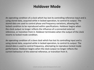
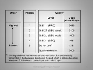
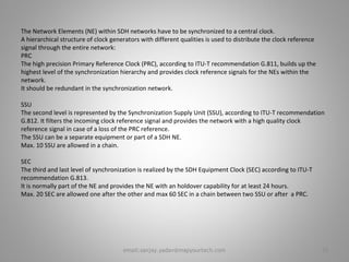
Synchronization Status Message (SSM)
It is defined in EN 300 417-6-1 [3]. This is a signal that is passed over a synchronization interface to indicate the
Quality-Level of the clock sourcing the synchronization signal. This signal was originally defined for use over
STM-N interfaces in the S1 byte. It has since been proposed for use over 2 Mbit/s interfaces as well.
The SSM code transmitted reflects the quality of the clock that the interface is ultimately traceable to; i.e. the
grade-of clock to which it is synchronized directly or indirectly via a chain of network element clock's (the
synchronization trail),or how long this chain of clocks is. For example, the clock-source quality-level may be a
Primary Reference Clock (PRC) complying with EN 300 462-6-1 [9], or it may be a Slave Clock in holdover-mode,
complying with ETSI EN 300 462-4-1 [7], or an EN 300 462-5-1 [8] Clock in holdover or free-run.
The clock-source quality-level is essentially, therefore, an indication only of the long-term accuracy of the
network element clock.
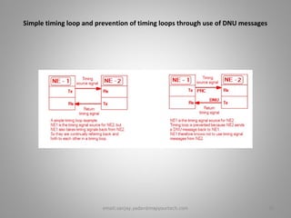
In a fully synchronized network all sources should be ultimately traceable to a PRC and this should be indicated
using a '0010' code. The "Do Not Use for Synchronization" code is used to prevent timing loops and is
transmitted in the opposite direction on interfaces used to synchronize an equipment's clock. The "Quality
Unknown" code was originally proposed for connection to equipment that did not use SSM codes. ETSI has
proposed that this coding is not used as it cannot be sensibly used in a quality based selection algorithm.
5email:sanjay.yadav@mapyourtech.com](https://image.slidesharecdn.com/synchronizationandtiminglooppresentation-mapyourtech-131008175803-phpapp02/85/Synchronization-and-timing-loop-presentation-mapyourtech-5-320.jpg)
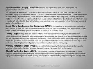
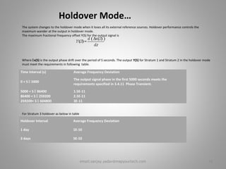
![SLIPS
The deletion and repetition of a data block is called a slip. If the block consists of only one bit, it is called a bit slip
or clock slip. If the block consists of an entire data frame (for example, the 192 payload bits in a DS1 frame), it is
called a frame slip. If the slip occurs at the frame boundary and the framing bit is not lost, it is called a controlled
slip. On the other hand, an uncontrolled slip means that identification of the frame boundary was lost and there
was a Change Of Frame Alignment (COFA). An uncontrolled slip is more serious because meaningful transmission
is interrupted (the receiver is unable to accurately read bit values) until framing is re-established.
The overall object of network synchronization is to minimize controlled slips and eliminate uncontrolled slips.
This can be achieved only by synchronizing all equipment clocks in all nodes to the same master clock or to a
number of master clocks that operate plesiochronously (very closely matched).Frame slips have different effects
on different traffic types. Table 1 shows the effects of a single frame slip on an individual 64 kb/s (DS-0) channel.
The slip rate between plesiochronous networks can be calculated from Eq. 1.
SR = Δf FR 86,400⋅ ⋅ Eq. 1
where
SR = Slip rate (frame slips/day)
Δf = Frequency accuracy difference
FR = Frame rate (frames/second) [Note: All telecommunications systems operate at 8,000 frames/second]
86,400 = Number of seconds/day
As an example, consider two networks that are synchronized by different clocks. One clock has
an accuracy of +1x10–11 and the other has an accuracy of –1x10–11. The accuracy difference in
this case is 2x10–11. Therefore, the slip rate is 2x10–11 x 8,000 frames/second x 86,400
seconds/day = 0.0138 frame slips/day, or 72.3 days/frame slip.
7email:sanjay.yadav@mapyourtech.com](https://image.slidesharecdn.com/synchronizationandtiminglooppresentation-mapyourtech-131008175803-phpapp02/85/Synchronization-and-timing-loop-presentation-mapyourtech-7-320.jpg)
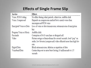
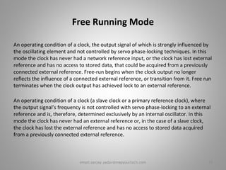
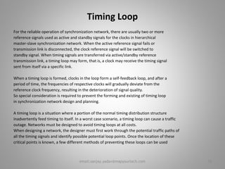
![Reference input signals:
T1, derived from:
STM-N (ITU-T Recommendation G.707 [18])
34 368 kbit/s with 125μs frame structure
139 264 kbit/s with 125μs frame structure
T2, derived from:
2 048 kbit/s (EN 300 166 [1])
T3, derived from:
2 048 kHz (EN 300 166 [1])
2 048 kbit/s (EN 300 166 [1]) with SSM according to (ITU-T Recommendation G.704 [16]).
Output signals:
T4: External reference signal,
2 048 kHz (ITU-T Recommendation G.703 [15]) (after physical interface)
2 048 kbit/s (EN 300 166 [1]) with SSM according to (ITU-T Recommendation G.704 [16]) (after
physical interface).
NOTE: The main application of 2 048 kbit/s signals with SSM is the exchange of synchronization status
information between an SSU and an SDH network element within a node.
T0: Timing signals for equipment-internal signal processing and for generating outgoing SDH traffic signals:
Frequencies are implementation-specific.
Basic properties for T0:
Frequency Accuracy: ± 4,6 × 10⁻⁶
Holdover: 5 × 10⁻⁸ (initial frequency offset)
2 × 10⁻⁶ (temperature)
1 × 10⁻⁸/day (aging)
10email:sanjay.yadav@mapyourtech.com](https://image.slidesharecdn.com/synchronizationandtiminglooppresentation-mapyourtech-131008175803-phpapp02/85/Synchronization-and-timing-loop-presentation-mapyourtech-10-320.jpg)


The document discusses synchronization in telecommunications networks. It defines key terms like synchronization status message (SSM), synchronization supply unit (SSU), primary reference clock (PRC), and timing loops. It explains that synchronization is important to avoid loss of information and describes the effects of poor synchronization. Slips, which are the deletion or repetition of data blocks, are discussed as well their impact on different traffic types. Maintaining synchronization across networks is necessary to minimize slips.