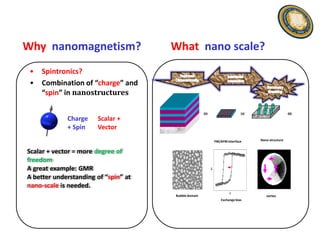
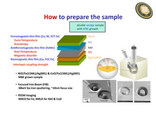
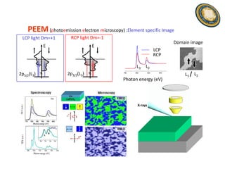
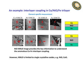
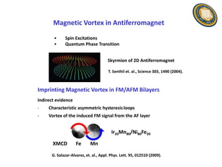
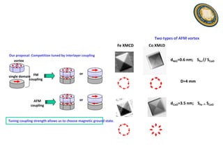
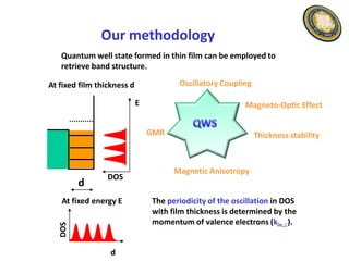
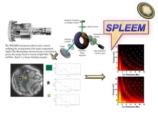
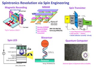
Very basic introduction to latest emerging technology in electronics called SPINTRONICS.
Quantum Mechanics property of electron called SPIN combine with the electronic property of electron .i.e SPIN+ELECTRONICS=SPINTRONICS
a branch of nano electronics that will improve technology by adding new freedom degrees to electronic for transfer and store information better than electronic devices :)
In our conventional electronic devices we use semi conducting materials for logical operation and magnetic materials for storage, but spintronics uses magnetic materials for both purposes. These spintronic devices are more versatile and faster than the present one. One such device is Spin Valve Transistors (SVT).
Spin valve transistor is different from conventional transistor. In this for conduction we use spin polarization of electrons. Only electrons with correct spin polarization can travel successfully through the device. These transistors are used in data storage, signal processing, automation and robotics with less power consumption and results in less heat. This also finds its application in Quantum computing, in which we use Qubits instead of bits.
IEEE presentation based on Spintronics & its semiconductor application specifically.
In the conclusion there is a hyperlink of a video which i'm unable to put here and hence i will give you the address of the video so that you can use the video and make the same hyperlink as i had made here.
TEDxCaltech-David Awschalom - Spintronics ( On YouTube)
video : 6:21- 7:13 (in video)
In this presentation file, i have briefly explained about Spintronics. it is a really new and a good concept for pressentation purpose. Hope it is helpful to you.
A small and brief introduction to spintronics and it's applications. Spintronics has tremendous applications in storage devices,Missile giudance, sensors etc.,
The magnetically sensitive transistor (also known as the spin transistor or spintronic transistor—named for spintronics, the technology which this development spawned), originally proposed in 1990 and currently still being developed, is an improved design on the common transistor invented in the 1940s. The spin transistor comes about as a result of research on the ability of electrons (and other fermions) to naturally exhibit one of two (and only two) states of spin: known as "spin up" and "spin down". Unlike its namesake predecessor, which operates on an electric current, spin transistors operate on electrons on a more fundamental level; it is essentially the application of electrons set in particular states of spin to store information.
Spintronics is a NANO technology which deals with spin dependent properties of an electron instead of charge dependent properties.
One of the main advantage of spintronics over electronics is the magnets tend to stay magnetize which is sparking in the industry an interest for replacing computer’s semiconductor based components with magnetic ones, starting with the RAM.
With an all-magnetic RAM, it is now possible to have a computer that retains all the information put into it. Most importantly, there will be no ‘boot-up’ waiting period when power is turned on.
Another promising feature of spintronics is that it doesn’t require the use of unique and specialized semiconductor, there by allowing it to work with common metals like Cu, Al, Ag.
Spintronics will use less power than conventional electronics, because the energy needed to change spin is a minute fraction of what is needed to push charge around.
Conventional electronic devices ignore the spin property and rely strictly on the transport of the electrical charge of electrons.
Adding the spin degree of freedom provides new effects, new capabilities and new functionalities.
nanotechnology has entered the sphere of water treatment processes. Many different types of nanomaterial’s are being evaluated and also being used in water treatment process.
Desalination is a key market area. Vast majority of worlds water is salt water, and though technology has existed for years that enables the desalination of ocean water, it is often a very energy intensive procedure and therefore expensive
Sebastiani - Nano-mechanical and microstructural characterization of MS-PVD N...thinfilmsworkshop
http://www.surfacetreatments.it/thinfilms
Nano-mechanical and microstructural characterization of MS-PVD Nb thin films (Marco Sebastiani - 30')
Speaker: Marco Sebastiani - Roma 3 University | Duration: 30 min.
Abstract
E. Bemporad1, M. Sebastiani1, F. Carassiti1
1Mechanical and Industrial Engineering Department, University of Rome ‘Roma Tre’, Via della Vasca Navale 79-00146 Rome, Italy
The main objective of the present study was to identify the influence of the applied bias voltage on the microstructural and mechanical properties of magnetron sputtering physical vapour deposition (MS-PVD) niobium thin films for use in superconducting resonant cavities for particle accelerators.
The microstructure and mechanical properties evolution as a function of the applied bias voltage and nature of the substrate (copper or quartz) were investigated by means of micro-hardness and nanoindentation testing, FIB/SEM, AFM and TEM techniques.
The superconducting properties (critical temperature Tc and residual resistivity) were determined by a calibrated four-contact probe and a cryogenic apparatus and then correlated to the mechanical properties.
Significant difference in terms of microstructure, surface roughness and mechanical properties were observed for biased coatings grown on different substrates. The observed differences are likely connected to the low conductivity of quartz that induces a re-sputtering effect and a consequent modification of the superconducting performances.
Introduction to nanoscience and nanotechnologyaimanmukhtar1
Introduction of nanoscience/nanotechnology ,properties/potential applications of nanomaterials and electrodeposition of metal single component and alloy nanowires in AAO template
Lattice Energy LLC-Technical Overview-June 25 2009Lewis Larsen
Commercializing a next generation source of safe nuclear energy: low energy nuclear reactions or LENRs. Widom-Larsen theory, weak interactions, transmutations, nanoscale evidence for nuclear effects, and Lattice's road to commercialization
New Explore Careers and College Majors 2024.pdfDr. Mary Askew
Explore Careers and College Majors is a new online, interactive, self-guided career, major and college planning system.
The career system works on all devices!
For more Information, go to https://bit.ly/3SW5w8W
Want to move your career forward? Looking to build your leadership skills while helping others learn, grow, and improve their skills? Seeking someone who can guide you in achieving these goals?
You can accomplish this through a mentoring partnership. Learn more about the PMISSC Mentoring Program, where you’ll discover the incredible benefits of becoming a mentor or mentee. This program is designed to foster professional growth, enhance skills, and build a strong network within the project management community. Whether you're looking to share your expertise or seeking guidance to advance your career, the PMI Mentoring Program offers valuable opportunities for personal and professional development.
Watch this to learn:
* Overview of the PMISSC Mentoring Program: Mission, vision, and objectives.
* Benefits for Volunteer Mentors: Professional development, networking, personal satisfaction, and recognition.
* Advantages for Mentees: Career advancement, skill development, networking, and confidence building.
* Program Structure and Expectations: Mentor-mentee matching process, program phases, and time commitment.
* Success Stories and Testimonials: Inspiring examples from past participants.
* How to Get Involved: Steps to participate and resources available for support throughout the program.
Learn how you can make a difference in the project management community and take the next step in your professional journey.
About Hector Del Castillo
Hector is VP of Professional Development at the PMI Silver Spring Chapter, and CEO of Bold PM. He's a mid-market growth product executive and changemaker. He works with mid-market product-driven software executives to solve their biggest growth problems. He scales product growth, optimizes ops and builds loyal customers. He has reduced customer churn 33%, and boosted sales 47% for clients. He makes a significant impact by building and launching world-changing AI-powered products. If you're looking for an engaging and inspiring speaker to spark creativity and innovation within your organization, set up an appointment to discuss your specific needs and identify a suitable topic to inspire your audience at your next corporate conference, symposium, executive summit, or planning retreat.
About PMI Silver Spring Chapter
We are a branch of the Project Management Institute. We offer a platform for project management professionals in Silver Spring, MD, and the DC/Baltimore metro area. Monthly meetings facilitate networking, knowledge sharing, and professional development. For event details, visit pmissc.org.
The Impact of Artificial Intelligence on Modern Society.pdfssuser3e63fc
Just a game Assignment 3
1. What has made Louis Vuitton's business model successful in the Japanese luxury market?
2. What are the opportunities and challenges for Louis Vuitton in Japan?
3. What are the specifics of the Japanese fashion luxury market?
4. How did Louis Vuitton enter into the Japanese market originally? What were the other entry strategies it adopted later to strengthen its presence?
5. Will Louis Vuitton have any new challenges arise due to the global financial crisis? How does it overcome the new challenges?Assignment 3
1. What has made Louis Vuitton's business model successful in the Japanese luxury market?
2. What are the opportunities and challenges for Louis Vuitton in Japan?
3. What are the specifics of the Japanese fashion luxury market?
4. How did Louis Vuitton enter into the Japanese market originally? What were the other entry strategies it adopted later to strengthen its presence?
5. Will Louis Vuitton have any new challenges arise due to the global financial crisis? How does it overcome the new challenges?
This comprehensive program covers essential aspects of performance marketing, growth strategies, and tactics, such as search engine optimization (SEO), pay-per-click (PPC) advertising, content marketing, social media marketing, and more
2. EDUCATION
Ph. D. CONDENSED PHYSICS
2007
HANYANG UNIVERSITY, Seoul, Korea TECHNICAL EXPERTISE
M. S. CONDENSED PHYSICS
1997 Instrument/ System development:
HONGIK UNIVERSITY, Seoul, Korea Development and construction of several vacuum
B. S. PHYSICS processing and measurement systems: UHV- STM, SMOKE,
1995 Electron-Beam Evaporation System.
ANDONG NATIONAL UNIVERSITY, Andong, Korea
Thin film growth:
Thermal E-beam evaporation systems. Thermal
RESEARCH EXPERIENCE Evaporation systems.
Department of Physics, University of California at Berkeley Structural and Surface analysis :
2009-present Low Energy Electron Diffraction (LEED), Atomic Force
Postdoctoral Associate, Advisor: Prof. Z. Q. Qiu Microscopy (AFM) , Scan Tunneling Microscopy (STM),
I investigated nano-magnetism in magnetic thin films. Photo Emission Electron Microscopy (PEEM), Scanning
Developed and built various vacuum processing and magnetic Electron Microscope (SEM).
measurement systems
Collaborated with various research partners (LBNL, UC DAVIS, and the Magnetic Characterization:
other UC Berkeley department) X-ray Magnetic Circular Dichroism (XMCD), X-ray Magnetic
Linear Dichroism (XMLD), Spin-Polarized Low Energy
Quantum Photonic Science Research Center in Hanyang University Electron Microscopy (SPLEEM), Superconducting Quantum
2006-2009 Interference Device (SQUID).
Additional Doctoral Research:
To further dissertation work, studied the fabrication of metallic thin
films and numerous Mn oxides, including magnetic alloy.
Korea Research Institute of Standards and Science
2003-2006
Additional Doctoral Research:
Investigated exchange bias effect of mono-layers of Fe on Pt (110) by
using In-situ SMOKE, XMCD, STM etc.
Developed and built UHV-STM and SMOKE measurement systems.
3. Why nanomagnetism? What nano scale?
• Spintronics?
• Combination of “charge” and
“spin” in nanostructures
2D 1D 0D
Charge Scalar +
+ Spin Vector
FM/AFM interface Nano-structure
Scalar + vector = more degree of
freedom
A great example: GMR
M
A better understanding of “spin” at
nano-scale is needed.
H
Bubble domain vortex
Exchange bias
4. How to prepare the sample
double wedge sample
with MBE growth
Ferromagnetic thin film (Co, Ni, FCT Fe)
Curie Temperature
Anisotropy
Antiferromagnetic thin film (FeMn)
Neel Temperature
Magnetic disorder
Nonmagnetic thin film (Cu, FCC Fe)
Interlayer coupling strength
• NiO/Fe(15ML)/Ag(001) & CoO/Fe(15ML)/Ag(001)
MBE grown sample
• Focused Iron Beam (FIB)
30keV Ga iron sputtering, ~10nm focus size
• PEEM imaging
XMCD for Fe; XMLD for NiO & CoO
m
5. PEEM (photoemission electron microscopy) :Element specific Image
LCP light Dm=+1 RCP light Dm=-1
Domain image
E E
LCP
Right
RCP
Left
L3 L2
2p3/2(L3) ~
~ 2p3/2(L3) ~
~
780 800 820
photo energy(eV)
840
L3 L2
Photon energy (eV)
Before
X-rays
After
6. An example: interlayer coupling in Co/NiO/Fe trilayer
Element-specific measurement
Co
NiO
Fe
Co
NiO
Fe
NiO XMLD image provides the key information to understand
the anomalous Co-Fe interlayer coupling.
However, XMLD is limited to single crystalline oxides, e.g. NiO, CoO.
7. Magnetic Vortex in Antiferromagnet
• Spin Excitations
• Quantum Phase Transition
Skyrmion of 2D Antiferromagnet
T. Senthil et. al., Science 303, 1490 (2004).
Imprinting Magnetic Vortex in FM/AFM Bilayers
Indirect evidence
- Characteristic asymmetric hysteresis loops
- Vortex of the induced FM signal from the AF layer
Ir20Mn80/Ni80Fe20
XMCD Fe Mn
G. Salazar-Alvarez, et. al., Appl. Phys. Lett. 95, 012510 (2009).
8. Two types of AFM vortex
Fe XMCD Co XMLD
Our proposal: Competition tuned by interlayer coupling
vortex dNiO=0.6 nm; SFe // SCoO
or
single domain FM
coupling
D=4 mm
AFM or
coupling
dCoO=3.5 nm; SFe ┴ SCoO
Tuning coupling strength allows us to choose magnetic ground state.
9. Our methodology
Quantum well state formed in thin film can be employed to
retrieve band structure.
At fixed film thickness d Oscillatory Coupling
E Magneto-Optic Effect
GMR Thickness stability
Magnetic Anisotropy
DOS
d
At fixed energy E The periodicity of the oscillation in DOS
with film thickness is determined by the
momentum of valence electrons (kin,).
DOS
d
10. 14
12
Energy (eV)
10
8
6
0 2 4 6 8 10 12
Co Thickness (ML)
14
12
Energy (eV)
10
8
6
0 2 4 6 8 10 12
Co Thickness (ML)
11. Spintronics Revolution via Spin Engineering
Magnetic Recording MRAM Spin Transistor
Spin-Valve Head
Pinned layer
Bit line
Current
“1” “0”
Memory cell
Word line with binary
information
Free layer • Density of DRAM
Tb/in2 before 2010 !
• Speed of SRAM IBM 256 Mb(’04)
• Non-volatility Samsung 64Kb(’03)
• Large Magnetocurrent(3500%)
• Low power • High Speed( 〉10GHz)
• Small collector current(~ 10 nA)
Biosensor
Spin LED Quantum Computer
Wang, INTERMAG(’03) Electron Spins in Quantum dots as Qubits
Ohno, Nature(’99)
13. Analysis of Cu(100nm)/Ru(3nm)/TaN(3nm)
/SiO(1um)/Si
SEM
No 3.
No 8.
No 9.
No10.
PEEM spectrum of elements
Distribution of Cu
Distribution of RuGeometry
Ru Cu O
No 10.
No 9.
450 480 925 950 490 560 630
14. Spin-Organic Light Emitting Diode
Cathode Interface
OLED • Metal Diffusion
light emission • Introduction of Impurities
• Barrier - poor e- injection
V Ferromagnetic metal cathodes
Spin Coated Polymer (Ir(ppy)3)
Spin coating process
ITO Glass substrate
- Fe, Al anode
Anode (ITO) Interface Rate: 5 A/s
• Indium, Oxygen Diffusion
• Barrier – poor h+ injection Base pressure: 10-7 Torr
• Variations in morphology - Organic layer
• Variations in work function Spin Coating 4000RPM
E-beam evaporation system
15. Two sepereated UHV STM systems
Variable temperature
SMOKE/LEED system Fe-Pt surface alloy: STM
Pt(110) surface: 1KeV Ar-ion sputtering
+ annealing at 1000 K
Fe evaporation: e-beam bombarded Fe plate (4N)
STM head and principle
Piezo
tube
200nm
Tip cartridge
Sample