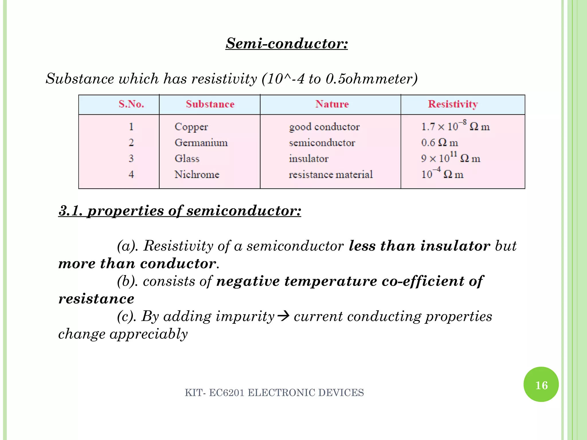
1
2
KIT- EC6201 ELECTRONIC DEVICES
DELIBERATION OF
TOPICS:
Atomic structure
Classification of solids
Semiconductor
3
KIT- EC6201 ELECTRONIC DEVICES
Atomic Structure:
1.1 Neils bhor theory:
Atom consists of
+ve charge  nucleus, -ve  electrons (revolve in circular
orbits).
Electron revolve around nucleus only in certain permitted orbits.
Each orbit certain fixed amount of energy.
Additional energy of electron excitation.
orbit name K,L,M,P…
Nucleus protons + neutrons.
Protons (positively charge), neutrons(neutral)
Atomic weight = no of protons + no of neutrons.
Atomic number = no of protons / no of electrons in atom
No of electrons in orbit2n2
4
KIT- EC6201 ELECTRONIC DEVICES
1.2. Structure of elements:
No of electrons in any orbit2n^2 nnumber of orbits
Example:
1st
 2 electrons
2nd
 8 electrons
3rd
 18 electrons
Atomic structure: ex copper
Atomic weight = 64
Atomic number =29
No of protons = no of electrons = 29
No of neutrons = 64-29 = 35
Electron29 1st
orbit2, 2nd
orbit8, 3rd
orbit18, 4th
orbit 1
5
KIT- EC6201 ELECTRONIC DEVICES
1.3 Electron:
tiny particles electrons
Negatively charged particle have negligible mass
Important properties:
Charge of electrons, e = 1.602 *10^-19 coulomb
Mass of electrons, m = 9.0*10^ -31kg
Radius of an electron, r = 1.9 * 10^-15meter
Ratio e/m of electron is 1.77*10^11coulombs/kg
mass of an electron is very small
very mobile and greatly influenced by electric or magnetic
fields
Energy of an electron:
2 types kinetic energy due to its motion
Potential energy due to charge on the nucleus
Total energy = K.E+P.E
Energy of electron increases as its distance from the nucleus
increases.
Last orbits electron possess very high energy as compared to electron
in the inner orbits.
6
KIT- EC6201 ELECTRONIC DEVICES
1.4 Energy band:
range of energy possessed by an electron in
a solid is known as energy bands
Each orbit of an atom has a single energy
7
KIT- EC6201 ELECTRONIC DEVICES
1.5 Energy band description:
Bands are classified into 2 types :
1.Valence band:
energy possessed by valence electron.
2.Conduction band:
energy possessed by free electron.
3.Forbidden energy gap:
separation between conduction band and
valance band on the energy level diagram.
width measures the bondage of valence
electrons to the atom.
8
KIT- EC6201 ELECTRONIC DEVICES
Classification of solids:
2.1.classification based on:
1.valance electrons
2.Free electrons
3.Forbidden energy gap
Valance electron:
determines the metal, non-metal, solids, gas, and electrical
properties of a material.
based on outermost valance electron.
Electrical conductivity of material are classified into
conductor
insulator
semi-conductor
Conductor:
valance electron < 4
Insulator:
valance electron > 4
Semi-conductor:
valance electron = 4
9
KIT- EC6201 ELECTRONIC DEVICES
Examples:
1.Conductor:
2.Insulator:
10
KIT- EC6201 ELECTRONIC DEVICES
3.semi-conductor:
11
KIT- EC6201 ELECTRONIC DEVICES
Free electrons:
valance electrons which are Loosely attached to the
nucleus
Conductor:
has large number of free electrons
Insulator:
has no free electrons
Semi-conductor:
has few free electrons
12
KIT- EC6201 ELECTRONIC DEVICES
Forbidden energy gap:
1.Insulator:
do not allow the passage of electric current
2.conductor:
which easily allow the passage of
electric current.
13
KIT- EC6201 ELECTRONIC DEVICES
3.Semi-conductor:
electrical conductivity lies in-
between conductor and insulator.
negative temperature co-
efficient of resistance.
14
KIT- EC6201 ELECTRONIC DEVICES
Why silicon is widely used as
semiconductor?
Answer is…….
15
KIT- EC6201 ELECTRONIC DEVICES
germanium valence electron  Higher energy level
16
KIT- EC6201 ELECTRONIC DEVICES
Semi-conductor:
Substance which has resistivity (10^-4 to 0.5ohmmeter)
3.1. properties of semiconductor:
(a). Resistivity of a semiconductor less than insulator but
more than conductor.
(b). consists of negative temperature co-efficient of
resistance
(c). By adding impurity current conducting properties
change appreciably
17
KIT- EC6201 ELECTRONIC DEVICES
3.2. Bonds in semiconductor:
Semi-conductor bonds  covalent bonds
18
KIT- EC6201 ELECTRONIC DEVICES
3.3. Effect of temperature on semiconductor:
(i).At absolute zero:
 act as perfect insulator
(ii).Above absolute zero:
 act as perfect conductor
19
KIT- EC6201 ELECTRONIC DEVICES
3.4.Hole current:
The current conduction by holes.
1. Due to movement of
valence electron from
one covalent bond to
another.
2. Current flow due to
presence of holes in
covalent bond
20
KIT- EC6201 ELECTRONIC DEVICES
3.4.Types of semi-conductor:
semi-conductor is classified as two type
(i).Intrinsic semi-conductor
(ii).Extrinsic semi-conductor
(i).Intrinsic semi-conductor:
extremely pure form of semiconductor
21
KIT- EC6201 ELECTRONIC DEVICES
(i).Extrinsic semi-conductor:
impure form of semiconductor
Doping:
adding impurity to the semiconductor
Two types of impurity:
1.Pentavalent impurity (donor impurity)
2.Trivalent impurity (acceptor impurity)
Pentavalent impurity  n-type semiconductor
Trivalent impurity  p- type semiconductor
N-type semiconductor:
22
KIT- EC6201 ELECTRONIC DEVICES
N-type conductivity:
current conduction predominantly by free electron
23
KIT- EC6201 ELECTRONIC DEVICES
P-type semi-conductor:
current conduction predominantly by holes
24
KIT- EC6201 ELECTRONIC DEVICES
P-type conductivity:
current conduction predominantly by holes
25
KIT- EC6201 ELECTRONIC DEVICES
Summarization of topics discussed:
1.Atomic structure
2. classification of solids
3.Semiconductors
26
KIT- EC6201 ELECTRONIC DEVICES

Semiconductor

  • 1.
  • 2.
    2 KIT- EC6201 ELECTRONICDEVICES DELIBERATION OF TOPICS: Atomic structure Classification of solids Semiconductor
  • 3.
    3 KIT- EC6201 ELECTRONICDEVICES Atomic Structure: 1.1 Neils bhor theory: Atom consists of +ve charge  nucleus, -ve  electrons (revolve in circular orbits). Electron revolve around nucleus only in certain permitted orbits. Each orbit certain fixed amount of energy. Additional energy of electron excitation. orbit name K,L,M,P… Nucleus protons + neutrons. Protons (positively charge), neutrons(neutral) Atomic weight = no of protons + no of neutrons. Atomic number = no of protons / no of electrons in atom No of electrons in orbit2n2
  • 4.
    4 KIT- EC6201 ELECTRONICDEVICES 1.2. Structure of elements: No of electrons in any orbit2n^2 nnumber of orbits Example: 1st  2 electrons 2nd  8 electrons 3rd  18 electrons Atomic structure: ex copper Atomic weight = 64 Atomic number =29 No of protons = no of electrons = 29 No of neutrons = 64-29 = 35 Electron29 1st orbit2, 2nd orbit8, 3rd orbit18, 4th orbit 1
  • 5.
    5 KIT- EC6201 ELECTRONICDEVICES 1.3 Electron: tiny particles electrons Negatively charged particle have negligible mass Important properties: Charge of electrons, e = 1.602 *10^-19 coulomb Mass of electrons, m = 9.0*10^ -31kg Radius of an electron, r = 1.9 * 10^-15meter Ratio e/m of electron is 1.77*10^11coulombs/kg mass of an electron is very small very mobile and greatly influenced by electric or magnetic fields Energy of an electron: 2 types kinetic energy due to its motion Potential energy due to charge on the nucleus Total energy = K.E+P.E Energy of electron increases as its distance from the nucleus increases. Last orbits electron possess very high energy as compared to electron in the inner orbits.
  • 6.
    6 KIT- EC6201 ELECTRONICDEVICES 1.4 Energy band: range of energy possessed by an electron in a solid is known as energy bands Each orbit of an atom has a single energy
  • 7.
    7 KIT- EC6201 ELECTRONICDEVICES 1.5 Energy band description: Bands are classified into 2 types : 1.Valence band: energy possessed by valence electron. 2.Conduction band: energy possessed by free electron. 3.Forbidden energy gap: separation between conduction band and valance band on the energy level diagram. width measures the bondage of valence electrons to the atom.
  • 8.
    8 KIT- EC6201 ELECTRONICDEVICES Classification of solids: 2.1.classification based on: 1.valance electrons 2.Free electrons 3.Forbidden energy gap Valance electron: determines the metal, non-metal, solids, gas, and electrical properties of a material. based on outermost valance electron. Electrical conductivity of material are classified into conductor insulator semi-conductor Conductor: valance electron < 4 Insulator: valance electron > 4 Semi-conductor: valance electron = 4
  • 9.
    9 KIT- EC6201 ELECTRONICDEVICES Examples: 1.Conductor: 2.Insulator:
  • 10.
    10 KIT- EC6201 ELECTRONICDEVICES 3.semi-conductor:
  • 11.
    11 KIT- EC6201 ELECTRONICDEVICES Free electrons: valance electrons which are Loosely attached to the nucleus Conductor: has large number of free electrons Insulator: has no free electrons Semi-conductor: has few free electrons
  • 12.
    12 KIT- EC6201 ELECTRONICDEVICES Forbidden energy gap: 1.Insulator: do not allow the passage of electric current 2.conductor: which easily allow the passage of electric current.
  • 13.
    13 KIT- EC6201 ELECTRONICDEVICES 3.Semi-conductor: electrical conductivity lies in- between conductor and insulator. negative temperature co- efficient of resistance.
  • 14.
    14 KIT- EC6201 ELECTRONICDEVICES Why silicon is widely used as semiconductor? Answer is…….
  • 15.
    15 KIT- EC6201 ELECTRONICDEVICES germanium valence electron  Higher energy level
  • 16.
    16 KIT- EC6201 ELECTRONICDEVICES Semi-conductor: Substance which has resistivity (10^-4 to 0.5ohmmeter) 3.1. properties of semiconductor: (a). Resistivity of a semiconductor less than insulator but more than conductor. (b). consists of negative temperature co-efficient of resistance (c). By adding impurity current conducting properties change appreciably
  • 17.
    17 KIT- EC6201 ELECTRONICDEVICES 3.2. Bonds in semiconductor: Semi-conductor bonds  covalent bonds
  • 18.
    18 KIT- EC6201 ELECTRONICDEVICES 3.3. Effect of temperature on semiconductor: (i).At absolute zero:  act as perfect insulator (ii).Above absolute zero:  act as perfect conductor
  • 19.
    19 KIT- EC6201 ELECTRONICDEVICES 3.4.Hole current: The current conduction by holes. 1. Due to movement of valence electron from one covalent bond to another. 2. Current flow due to presence of holes in covalent bond
  • 20.
    20 KIT- EC6201 ELECTRONICDEVICES 3.4.Types of semi-conductor: semi-conductor is classified as two type (i).Intrinsic semi-conductor (ii).Extrinsic semi-conductor (i).Intrinsic semi-conductor: extremely pure form of semiconductor
  • 21.
    21 KIT- EC6201 ELECTRONICDEVICES (i).Extrinsic semi-conductor: impure form of semiconductor Doping: adding impurity to the semiconductor Two types of impurity: 1.Pentavalent impurity (donor impurity) 2.Trivalent impurity (acceptor impurity) Pentavalent impurity  n-type semiconductor Trivalent impurity  p- type semiconductor N-type semiconductor:
  • 22.
    22 KIT- EC6201 ELECTRONICDEVICES N-type conductivity: current conduction predominantly by free electron
  • 23.
    23 KIT- EC6201 ELECTRONICDEVICES P-type semi-conductor: current conduction predominantly by holes
  • 24.
    24 KIT- EC6201 ELECTRONICDEVICES P-type conductivity: current conduction predominantly by holes
  • 25.
    25 KIT- EC6201 ELECTRONICDEVICES Summarization of topics discussed: 1.Atomic structure 2. classification of solids 3.Semiconductors
  • 26.