A 10 d bm 25 dbm, 0.363 mm2 two stage 130 nm rf cmos power amplifierVLSICS Design
This paper proposes a 2.4 GHz RF CMOS Power amplifi
er and variation in its main performance
parameters i.e, output power, S-parameters and powe
r added efficiency with respect to change in supply
voltage and size of the power stage transistor. The
supply voltage was varied form 1 V to 5 V and the
range
of output power at 1dB compression point was found
to be from 10.684 dBm to 25.08 dBm respectively.
The range of PAE is 16.65 % to 48.46 %. The width o
f the power stage transistor was varied from 150 μm
to 500 μm to achieve output power of range 15.47 dB
m to 20.338 dBm. The range of PAE obtained here is
29.085 % to 45.439 %. The total dimension of the la
yout comes out to be 0.714 * 0.508 mm
2
.
IJRET : International Journal of Research in Engineering and Technology is an international peer reviewed, online journal published by eSAT Publishing House for the enhancement of research in various disciplines of Engineering and Technology. The aim and scope of the journal is to provide an academic medium and an important reference for the advancement and dissemination of research results that support high-level learning, teaching and research in the fields of Engineering and Technology. We bring together Scientists, Academician, Field Engineers, Scholars and Students of related fields of Engineering and Technology.
A 60 GHz CMOS Power Amplifier for Wireless CommunicationsIJECEIAES
This paper presents a 60 GHz power amplifier (PA) suitable for wireless communications. The two-stage wideband PA is fabricated in 55 nm CMOS. Measurement results show that the PA obtains a peak gain of 16 dB over a -3 dB bandwidth from 57 GHz to 67 GHz. It archives an output 1 dB compression point (OP1dB) of 4 dBm and a peak power added efficiency (PAE) of 12.6%. The PA consumes a total DC power of 38.3 mW from a 1.2 V supply voltage while its core occupies a chip area of 0.45 mm 2 .
An operational amplifier with recycling folded cascode topology and adaptive ...VLSICS Design
This paper presents a highly adaptive operational amplifier with high gain, high bandwidth, high speed
and low power consumption. By adopting the recycling folded cascode topology along with an adaptivebiasing
circuit, this design achieves high performance in terms of gain-bandwidth product (GBW) and slew
rate (SR). This single stage op-amp has been designed in 0.18μm technology with a power supply of 1.8V
and a 5pF load. The simulation results show that the amplifier achieved a GBW of 335.5MHz, Unity Gain
Bandwidth of 247.1MHz and a slew rate of 92.8V/μs.
A New CMOS Fully Differential Low Noise Amplifier for Wideband ApplicationsTELKOMNIKA JOURNAL
In this paper, a multi-stage fully differential low noise amplifier (LNA) has been presented for
wideband applications. A common-gate input stage is used to improve the input impedance matching and
linearity. A common-source stage is also used as the second stage to enhance gain and reduce noise. A
shunt-shunt feedback is employed to extend bandwidth and enhance linearity. The proposed low noise
amplifier has been designed and simulated using RF-TSMC 0.18 μm CMOS process technology. In
frequency band of 3.5-7.5 GHz, this amplifier has a flat power gain (S21) of 16.5 ± 1.5 dB, low noise figure
(NF) of 3dB, input (S11) and output (S22) return losses less than -10 dB and high linearity with input thirdorder
intercept point (IIP3) of -3dBm. It’s power consumption is also less than 10 mw with low power supply
voltage of 0.8v.
Open Loop Control Of Series Parallel Resonant ConverterIDES Editor
Resonant converters are desirable for power
conversion due to their comparatively smaller size and
lower power losses resulting from high-frequency
operation and inherent soft switching. Among all the
topologies of the resonant converters, the series–parallel
resonant converter (SPRC) is known to have the
combined merits of the series resonant converter and
parallel resonant converter. The converter can regulate
the output voltage at a constant switching frequency even
for a change in load resistance from full load resistance to
infinity while maintaining good part load efficiency. The
purpose of this project is to design a closed loop
controller for the phase-controlled series parallel
resonant converter (PC SPRC). The open loop analysis
and closed loop control has been provided in this paper.
Design of Low Power & High Speed Comparator with 0.18μm Technology for ADC Ap...IJERA Editor
In Analog to Digital Converter (ADC), high speed comparator influences the overall performance of ADC directly. This paper presents the high speed & low power design of a CMOS comparator. Schematic design of this comparator is fabricated in a 0.18μm UMC Technology with 1.8V power supply and simulated in cadence Virtuoso. Simulation results are presented and it shows that this design can work under high speed of 0.8108 GHz. The design has a low offset voltage, low power dissipation 108.0318μw. In addition we have verified present results with schematic view design and also compared these results with earlier reported work and got improvement in this reported work.
Double feedback technique for reduction of Noise LNA with gain enhancementijceronline
In this paper we present a balun low noise amplifier (LNA) in which the gain is boosted by using a double feedback structure. The circuit is based on a conventional balun LNA with noise and distortion cancelation. The LNA is based on the combination of a common-gate (CG) stage and common-source (CS) stage. We propose to replace the load resistors by active loads, which can be used to implement local feedback loops (in the CG and CS stages). This will boost the gain and reduce the noise figure (NF). Simulation results, with a 130nm CMOS technology, show that the gain is 24dB and the NF is less than 2.7dB. The total power dissipation is only 5.4mW (since no extra blocks are required), leading to a figure-of-merit (FOM) of 3.8mW-1 using a nominal 1.2V supply. Measurement results are presented for the proposed DFBLNA included in a receiver frontend for biomedical applications (ISM and WMTS).
Design of a low-power compact CMOS variable gain amplifier for modern RF rece...journalBEEI
The demand for portability has speeded up the design of low-power electronic communication devices. Variable gain amplifier (VGA) is one of the most vulnerable elements of every modern receiver for the proper baseband processing of the signal. CMOS VGAs are generally suffered from low bandwidth and small gain range. In this research, a two-stage class AB VGA, each stage comprising of a direct transconductance amplifier and a linear transimpedance amplifier, is designed in Silterra 0.13-μm CMOS utilizing Mentor Graphics environment. The post-layout simulation results reveal that the VGA design achieves the widest bandwidth of >200 MHz and high gain range from -33 to 32 dB. The VGA dissipates only 2mW from a single 1.2 V DC supply. The core chip area of the VGA is also only 0.026 mm2 which is also the lowest compared to recent researches. Such a VGA will be a very useful module for all modern communication devices.
DESIGN OF 2.4 GHZ MMIC FEED FORWARD AMPLIFIER FOR WIRELESS APPLICATIONS jmicro
This paper proposes a design of 0.15μm Monolithic Microwave Integrated Circuit (MMIC) power amplifier
using GaAs pHEMT technology at 2.4 GHz which employs feed forward linearization technique to improve
linearity. The amplifier is designed to operate in personal communication systems (PCS) frequency range
using WIN semiconductor GaAs pHEMT technology. Single stage power amplifier is designed in lumped
and distributed components with its layout. Linearity of PA is improved by Feed forward Linearization
technique. To evaluate the performance of proposed linearized amplifier, Advanced Design system (ADS)
tool is used. The designed circuit results with 13.65dBm output power at 1dB compression point (P1dB),
6dB power gain and maximum Power added efficiency of 16.4%. Linearity achieved by feed forward
linearizer circuit with third order intermodulation suppression of 30dBc for the output power level of
8.217dBm and 1dB compression point at an input power of 15 dBm whereas 6 dBm for the Power amplifier
without feed forward linearizer circuit. The designed Power amplifier system with feed forward linearizer
had IMD3 suppression of 30dBc which is in appreciable range with improvement in 1dB compression
point.
Design of a high frequency low voltage CMOS operational amplifierVLSICS Design
A method is presented in this paper for the design of a high frequency CMOS operational amplifier (OpAmp) which operates at 3V power supply using tsmc 0.18 micron CMOS technology. The OPAMP designed is a two-stage CMOS OPAMP followed by an output buffer. This Operational Transconductance Amplifier (OTA) employs a Miller capacitor and is compensated with a current buffer compensation technique. The unique behaviour of the MOS transistors in saturation region not only allows a designer to work at a low voltage, but also at a high frequency. Designing of two-stage op-amps is a multi-dimensional-optimization problem where optimization of one or more parameters may easily result into degradation of others. The OPAMP is designed to exhibit a unity gain frequency of 2.02GHz and exhibits a gain of 49.02dB with a 60.50 phase margin. As compared to the conventional approach, the proposed compensation method results in a higher unity gain frequency under the same load condition. Design has been carried out in Tanner tools. Simulation results are verified using S-edit and W-edit.
DESIGN OF 2.4 GHZ MMIC FEED FORWARD AMPLIFIER FOR WIRELESS APPLICATIONS jmicro
This paper proposes a design of 0.15μm Monolithic Microwave Integrated Circuit (MMIC) power amplifier using GaAs pHEMT technology at 2.4 GHz which employs feed forward linearization technique to improve linearity. The amplifier is designed to operate in personal communication systems (PCS) frequency range using WIN semiconductor GaAs pHEMT technology. Single stage power amplifier is designed in lumped and distributed components with its layout. Linearity of PA is improved by Feed forward Linearization technique. To evaluate the performance of proposed linearized amplifier, Advanced Design system (ADS) tool is used. The designed circuit results with 13.65dBm output power at 1dB compression point (P1dB), 6dB power gain and maximum Power added efficiency of 16.4%. Linearity achieved by feed forward linearizer circuit with third order intermodulation suppression of 30dBc for the output power level of 8.217dBm and 1dB compression point at an input power of 15 dBm whereas 6 dBm for the Power amplifier without feed forward linearizer circuit. The designed Power amplifier system with feed forward linearizer had IMD3 suppression of 30dBc which is in appreciable range with improvement in 1dB compression point
DESIGN OF 2.4 GHZ MMIC FEED FORWARD AMPLIFIER FOR WIRELESS APPLICATIONSjmicro
This paper proposes a design of 0.15μm Monolithic Microwave Integrated Circuit (MMIC) power amplifier
using GaAs pHEMT technology at 2.4 GHz which employs feed forward linearization technique to improve
linearity. The amplifier is designed to operate in personal communication systems (PCS) frequency range
using WIN semiconductor GaAs pHEMT technology. Single stage power amplifier is designed in lumped
and distributed components with its layout. Linearity of PA is improved by Feed forward Linearization
technique. To evaluate the performance of proposed linearized amplifier, Advanced Design system (ADS)
tool is used. The designed circuit results with 13.65dBm output power at 1dB compression point (P1dB),
6dB power gain and maximum Power added efficiency of 16.4%. Linearity achieved by feed forward
linearizer circuit with third order intermodulation suppression of 30dBc for the output power level of
8.217dBm and 1dB compression point at an input power of 15 dBm whereas 6 dBm for the Power amplifier
without feed forward linearizer circuit. The designed Power amplifier system with feed forward linearizer
had IMD3 suppression of 30dBc which is in appreciable range with improvement in 1dB compression
point.
0.5GHz - 1.5GHz Bandwidth 10W GaN HEMT RF Power Amplifier Design IJECEIAES
With the current development in wireless communication technology, the need for a wide bandwith in RF power amplifier (RF PA) is an essential. In this paper, the design and simulation of 10W GaN HEMT wideband RF PA will be presented. The Source-Pull and Load-Pull technique was used to design the input and output matching network of the RF PA. From the simulation, the RF PA achieved a flat gain between 15dB to 17dB from 0.5GHz to 1.5GHz. At 1.5GHz, the drain efficiency is simulated to achieve 36% at the output power of 40 dBm while the power added efficiency (PAE) was found to be 28.2%.
IOSR Journal of Electronics and Communication Engineering(IOSR-JECE) is an open access international journal that provides rapid publication (within a month) of articles in all areas of electronics and communication engineering and its applications. The journal welcomes publications of high quality papers on theoretical developments and practical applications in electronics and communication engineering. Original research papers, state-of-the-art reviews, and high quality technical notes are invited for publications.
A Novel Design of a Microstrip Microwave Power Amplifier for DCS Application ...IJECEIAES
This paper presents a 1.80GHz class-A Microwave power amplifier (PA). The proposed power amplifier is designed with single-stage architecture. This power amplifier consists of a bipolar transistor and improved by Collector-Feedback Biasing fed with a single power supply. The aim of this work is to improve the performance of this amplifier by using simple stubs with 50Ω microstrip transmissions lines. The proposed PA is investigated and optimized by utilizing Advanced Design System (ADS) software. The simulation results show that the amplifier achieves a high power gain of 13dB, output power rise up to 21dBm and good impedances matching ;For the input reflection coefficient (S11) is below than - 46.39dB. Regarding the output reflection coefficient (S22) is below than -29.898dB, with an overall size of about 93 x 59mm². By the end; we find that this power amplifier offers an excellent performance for DCS applications.
International Journal of Engineering and Science Invention (IJESI)inventionjournals
International Journal of Engineering and Science Invention (IJESI) is an international journal intended for professionals and researchers in all fields of computer science and electronics. IJESI publishes research articles and reviews within the whole field Engineering Science and Technology, new teaching methods, assessment, validation and the impact of new technologies and it will continue to provide information on the latest trends and developments in this ever-expanding subject. The publications of papers are selected through double peer reviewed to ensure originality, relevance, and readability. The articles published in our journal can be accessed online.
IJRET : International Journal of Research in Engineering and Technology is an international peer reviewed, online journal published by eSAT Publishing House for the enhancement of research in various disciplines of Engineering and Technology. The aim and scope of the journal is to provide an academic medium and an important reference for the advancement and dissemination of research results that support high-level learning, teaching and research in the fields of Engineering and Technology. We bring together Scientists, Academician, Field Engineers, Scholars and Students of related fields of Engineering and Technology
This paper proposes a new voltage frequency converter (VFC) that converts both voltage and frequency to the required level of voltage and frequency in low voltage networks used in various countries. The proposed converter could be used as a universal power supply for sensitive AC loads. The converter is composed of, input voltage and frequency detection circuitry, full bridge boost rectifier and a DC to AC inverter. In addition, to improve the feasibility and performance of the converter, synchronous reference based PI (SRFPI) controller is adopted, where the system behaves similar to a DC-DC converter. The parameter selection of PI controller is done using a recent optimisation technique called Lightning Search Algorithm (LSA). The simulation of VFC is conducted in MATLAB/Simulink environment. The simulation results shows that LSA based PI controller provides better output voltage regulation with respect to the reference value under various load and input conditions.
IJERA (International journal of Engineering Research and Applications) is International online, ... peer reviewed journal. For more detail or submit your article, please visit www.ijera.com
Phase Frequency Detector and Charge Pump for Low Jitter PLL Applications IJECEIAES
In this paper a new technique is presented to improve the jitter performance of conventional phase frequency detectors by completely removing the unnecessary one-shot pulse. This technique uses a variable pulse-height circuit to control the unnecessary one-shot pulse height. In addition, a novel charge-pump circuit with perfect current-matching characteristics is used to improve the output jitter performance of conventional charge pumps. This circuit is composed of a pair of symmetrical pump circuits to obtain a good current matching. As a result, the proposed charge-pump circuit has perfect current-matching characteristics, wide output range, no glitch output current, and no jump output voltage. In order to verify such operation, circuit simulation is performed using 0.18 μm CMOS process parameters.
A Five – Level Integrated AC – DC ConverterIJTET Journal
This paper presents the implementation of a new five – level integrated AC – DC converter with high input power factor and reduced input current harmonics complied with IEC1000-3-2 harmonic standards for electrical equipments. The proposed topology is a combination of boost input power factor pre – regulator and five – level DC – DC converter. The single – stage PFC (SSPFC) approach used in this topology is an alternative solution to low – power and cost – effective applications.
Research Inventy : International Journal of Engineering and Scienceresearchinventy
Research Inventy : International Journal of Engineering and Science is published by the group of young academic and industrial researchers with 12 Issues per year. It is an online as well as print version open access journal that provides rapid publication (monthly) of articles in all areas of the subject such as: civil, mechanical, chemical, electronic and computer engineering as well as production and information technology. The Journal welcomes the submission of manuscripts that meet the general criteria of significance and scientific excellence. Papers will be published by rapid process within 20 days after acceptance and peer review process takes only 7 days. All articles published in Research Inventy will be peer-reviewed.
Between Filth and Fortune- Urban Cattle Foraging Realities by Devi S Nair, An...Mansi Shah
This study examines cattle rearing in urban and rural settings, focusing on milk production and consumption. By exploring a case in Ahmedabad, it highlights the challenges and processes in dairy farming across different environments, emphasising the need for sustainable practices and the essential role of milk in daily consumption.
PDF SubmissionDigital Marketing Institute in NoidaPoojaSaini954651
https://www.safalta.com/online-digital-marketing/advance-digital-marketing-training-in-noidaTop Digital Marketing Institute in Noida: Boost Your Career Fast
[3:29 am, 30/05/2024] +91 83818 43552: Safalta Digital Marketing Institute in Noida also provides advanced classes for individuals seeking to develop their expertise and skills in this field. These classes, led by industry experts with vast experience, focus on specific aspects of digital marketing such as advanced SEO strategies, sophisticated content creation techniques, and data-driven analytics.
Technoblade The Legacy of a Minecraft Legend.Techno Merch
Technoblade, born Alex on June 1, 1999, was a legendary Minecraft YouTuber known for his sharp wit and exceptional PvP skills. Starting his channel in 2013, he gained nearly 11 million subscribers. His private battle with metastatic sarcoma ended in June 2022, but his enduring legacy continues to inspire millions.
EASY TUTORIAL OF HOW TO USE CAPCUT BY: FEBLESS HERNANEFebless Hernane
CapCut is an easy-to-use video editing app perfect for beginners. To start, download and open CapCut on your phone. Tap "New Project" and select the videos or photos you want to edit. You can trim clips by dragging the edges, add text by tapping "Text," and include music by selecting "Audio." Enhance your video with filters and effects from the "Effects" menu. When you're happy with your video, tap the export button to save and share it. CapCut makes video editing simple and fun for everyone!
Can AI do good? at 'offtheCanvas' India HCI preludeAlan Dix
Invited talk at 'offtheCanvas' IndiaHCI prelude, 29th June 2024.
https://www.alandix.com/academic/talks/offtheCanvas-IndiaHCI2024/
The world is being changed fundamentally by AI and we are constantly faced with newspaper headlines about its harmful effects. However, there is also the potential to both ameliorate theses harms and use the new abilities of AI to transform society for the good. Can you make the difference?
Connect Conference 2022: Passive House - Economic and Environmental Solution...TE Studio
Passive House: The Economic and Environmental Solution for Sustainable Real Estate. Lecture by Tim Eian of TE Studio Passive House Design in November 2022 in Minneapolis.
- The Built Environment
- Let's imagine the perfect building
- The Passive House standard
- Why Passive House targets
- Clean Energy Plans?!
- How does Passive House compare and fit in?
- The business case for Passive House real estate
- Tools to quantify the value of Passive House
- What can I do?
- Resources
Transforming Brand Perception and Boosting Profitabilityaaryangarg12
In today's digital era, the dynamics of brand perception, consumer behavior, and profitability have been profoundly reshaped by the synergy of branding, social media, and website design. This research paper investigates the transformative power of these elements in influencing how individuals perceive brands and products and how this transformation can be harnessed to drive sales and profitability for businesses.
Through an exploration of brand psychology and consumer behavior, this study sheds light on the intricate ways in which effective branding strategies, strategic social media engagement, and user-centric website design contribute to altering consumers' perceptions. We delve into the principles that underlie successful brand transformations, examining how visual identity, messaging, and storytelling can captivate and resonate with target audiences.
Methodologically, this research employs a comprehensive approach, combining qualitative and quantitative analyses. Real-world case studies illustrate the impact of branding, social media campaigns, and website redesigns on consumer perception, sales figures, and profitability. We assess the various metrics, including brand awareness, customer engagement, conversion rates, and revenue growth, to measure the effectiveness of these strategies.
The results underscore the pivotal role of cohesive branding, social media influence, and website usability in shaping positive brand perceptions, influencing consumer decisions, and ultimately bolstering sales and profitability. This paper provides actionable insights and strategic recommendations for businesses seeking to leverage branding, social media, and website design as potent tools to enhance their market position and financial success.
Book Formatting: Quality Control Checks for DesignersConfidence Ago
This presentation was made to help designers who work in publishing houses or format books for printing ensure quality.
Quality control is vital to every industry. This is why every department in a company need create a method they use in ensuring quality. This, perhaps, will not only improve the quality of products and bring errors to the barest minimum, but take it to a near perfect finish.
It is beyond a moot point that a good book will somewhat be judged by its cover, but the content of the book remains king. No matter how beautiful the cover, if the quality of writing or presentation is off, that will be a reason for readers not to come back to the book or recommend it.
So, this presentation points designers to some important things that may be missed by an editor that they could eventually discover and call the attention of the editor.
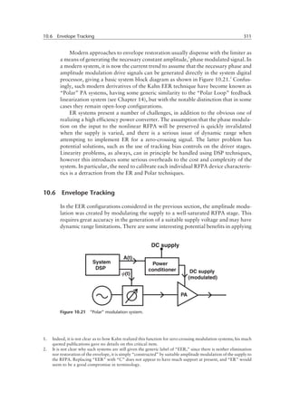
Rf power amplifiers for wireless communications ch10 6
1. Modern approaches to envelope restoration usually dispense with the limiter as
a means of generating the necessary constant amplitude,
1
phase modulated signal. In
a modern system, it is now the current trend to assume that the necessary phase and
amplitude modulation drive signals can be generated directly in the system digital
processor, giving a basic system block diagram as shown in Figure 10.21.2
Confus-
ingly, such modern derivatives of the Kahn EER technique have become known as
“Polar” PA systems, having some generic similarity to the “Polar Loop” feedback
linearization system (see Chapter 14), but with the notable distinction that in some
cases they remain open-loop configurations.
ER systems present a number of challenges, in addition to the obvious one of
realizing a high efficiency power converter. The assumption that the phase modula-
tion on the input to the nonlinear RFPA will be preserved is quickly invalidated
when the supply is varied, and there is a serious issue of dynamic range when
attempting to implement ER for a zero-crossing signal. The latter problem has
potential solutions, such as the use of tracking bias controls on the driver stages.
Linearity problems, as always, can in principle be handled using DSP techniques,
however this introduces some serious overheads to the cost and complexity of the
system. In particular, the need to calibrate each individual RFPA device characteris-
tics is a detraction from the ER and Polar techniques.
10.6 Envelope Tracking
In the EER configurations considered in the previous section, the amplitude modu-
lation was created by modulating the supply to a well-saturated RFPA stage. This
requires great accuracy in the generation of a suitable supply voltage and may have
dynamic range limitations. There are some interesting potential benefits in applying
10.6 Envelope Tracking 311
Figure 10.21 “Polar” modulation system.
1. Indeed, it is not clear as to how Kahn realized this function for zero-crossing modulation systems; his much
quoted publications gave no details on this critical item.
2. It is not clear why such systems are still given the generic label of “EER,” since there is neither elimination
nor restoration of the envelope, it is simply “constructed” by suitable amplitude modulation of the supply to
the RFPA. Replacing “EER” with “C” does not appear to have much support at present, and “ER” would
seem to be a good compromise in terminology.
2. a similar envelope-derived modulation to the supply voltage of a conventional linear
RF amplifier. Such a technique is generally termed “Envelope Tracking,” or “ET,”
and is shown schematically in Figure 10.22.
Recalling the analysis of a conventional Class B amplifier (Figure 10.1), we have
already seen that if the RF load resistor is decreased in inverse proportion to increas-
ing drive voltage amplitude, the efficiency remains constant at its maximum value
while the power increases as the square root of the drive power; this is an important
mode of dynamic behavior in the Doherty amplifier (Section 10.2). An alternative,
and considerably simpler, scenario is that the load resistor remains fixed and the
supply voltage is increased in proportion to the increasing drive voltage. In this case,
maximum efficiency is maintained (due to full rail-to-rail voltage swing) and the
output power increases linearly with input drive power. This process can be contin-
ued down to a selected point on the lower side, and up to a point where the RF swing
reaches breakdown level. In this manner, maximum efficiency can be maintained
over a wide linear power range.
One of the appealing aspects of this technique is that the modulation control
voltage does not have to replicate the signal envelope with great accuracy, as is the
case in the ER process. For example, the supply voltage could be tracked for just the
upper few dB of the signal envelope range; this would then show an overall PBO effi-
ciency characteristic somewhat comparable to a Doherty PA. The still-present chal-
lenge of the tracking power converter can also be further reduced by the use of a
power supply having two or more discrete switched output voltage levels. Problems
of dynamic range, particularly in zero-crossing signal environments, are essentially
eliminated by allowing for normal linear operation at a reduced supply voltage in
the small signal regime. An additional attraction of ET is that the efficiency enhance-
ment process is completely decoupled
3
from the RF matching. This is in contrast to
the Doherty and Chireix configurations, which depend heavily for their operation
on resonant RF circuit elements.
It is instructive to consider a simple case, where two supply voltages are avail-
able, as shown in Figure 10.23. The supply switch can, in principle, be realized using
low cost and readily available semiconductors, which for envelope speeds in the
MHz range do not have to be exceptionally fast, by modern standards. The drive
signal to the switch would conventionally be derived by using an envelope detector
312 Efficiency Enhancement Techniques
RF IN
DC
RF OUT
Pwr. cond
Figure 10.22 Envelope Tracking (“ET”) RF PA system.
3. Both literally and metaphorically; the physical integration of power converter and RFPA circuitry is one of
the less publicized challenges in implementing ER systems.
3. and a threshold circuit which sets the level at which the switch was activated. A
modern implementation would probably use a drive signal generated by the system
DSP, which could conveniently be time-synchronized with appropriate pre-
distortion of the input RF signal. This will include necessary compensation for the
small changes in gain and phase in the RFPA as the supply is switched. The “break-
point,” or envelope level at which the supply is switched, is clearly an important
design choice. This choice will have an optimum value, dependent on the statistics
of the signal environment. As with the selection of the breakpoint in a Doherty PA,
the intuitive choice would be to set the lower voltage to switch in at the mean power
level, the higher supply being used up to the peak power. The efficiency characteris-
tic shown in Figure 10.24 assumes that the PA follows the ideal Class B PBO/effi-
ciency characteristic for each supply voltage setting, reaching a maximum value of
70% at the onset of envelope clipping in each case.
In order to evaluate the impact of such a characteristic in a specific signal envi-
ronment, it is necessary to generate a representative signal burst and evaluate the
average efficiency. This process can be repeated for various breakpoint and PEP
backoff settings. For example, Figure 10.25 shows the results from performing this
exercise for a two-level supply voltage on an EDGE signal. The average efficiency
10.6 Envelope Tracking 313
RF IN
Switch drive
DC
RF OUT
DC-DC conv.
Figure 10.23 ET System using a two-level switched supply.
100
50
0
-10 dB-20 dB Pmax
Efficiency
(%)
Output power
backoff (dB)
Vss
Vss/2Vss/3
Figure 10.24 PBO-Efficiency characteristic for two-level switched ET system.
4. for the two-level supply switch is plotted for a range of breakpoint values. It is clear
that a simple two-level switch, in this signal environment, can give a useful increase
in efficiency (53.5% at optimum break point) in comparison to a standard Class B
PA (45.3%), but falls significantly short of the Doherty PA result for the same signal
environment (60.3%). In the case of an EDGE signal, it will in practice be necessary
to back the PEP level down from the clipping point in order to obtain acceptable
ACP performance, this will reduce all of the efficiency results by a similar factor.
The efficiency gains in Figure 10.25 seem to deliver somewhat less than the PBO effi-
ciency curves might suggest. The returns are, however, quite critically dependent on
the signal environment. Some further details of the method used to perform the effi-
ciency computations contained in Figure 10.25, and some more simulation results,
will be presented in Section 10.10.
As is customary when promoting efficiency enhancement techniques, little has
been said about the possible effects of the technique on the PA linearity. As far as
envelope tracking is concerned, this has to be raised as a potentially serious issue.
The next chapter in this book, Chapter 11, is largely devoted to minimizing the
harmful effects of small amounts of unintended modulation on the supply voltage to
an RFPA. Clearly, when it is proposed that this same supply voltage be intentionally
yanked around over most of its allowable range in order to improve the efficiency,
questions about linearity have to be addressed. The standard answer, as always in
the modern era, is that DSP will save the day. The gain and phase variations which
the tracking will create can in principle be characterized and compensated by suit-
able adjustment (DPD) to the input signal. But there can be little doubt that the large
supply variations will make the DPD task more challenging.
10.7 Power Converters for EER and ET
The implementation of a high efficiency, broadband power converter design for
EER and ET implementation in RFPAs has been the focus of much research activity
314 Efficiency Enhancement Techniques
Break point (normalized)
Efficiency
(%)
100
50
0
0 0.5 1.0
Doherty (6 dB breakpoint)
Figure 10.25 Average efficiency for EDGE signal, Class B PA with switched voltage supply;
(switch break point plotted as x-axis). Doherty PA efficiency shown for standard 6 dB break point.