The document discusses the use of cascaded T-type multilevel inverters (CTB-MLIs) in grid-connected photovoltaic (PV) systems, highlighting their advantages in reducing harmonic distortion and improving power quality. It presents a comparative analysis of various inverter topologies and their components, emphasizing the importance of efficient maximum power point tracking (MPPT) techniques. The work underscores the potential of renewable energy systems, particularly solar-based technologies, in addressing environmental challenges and enhancing energy security.
![International Journal of Trend in Scientific Research and Development (IJTSRD)
Volume 7 Issue 1, January-February 2023 Available Online: www.ijtsrd.com e-ISSN: 2456 – 6470
@ IJTSRD | Unique Paper ID – IJTSRD52629 | Volume – 7 | Issue – 1 | January-February 2023 Page 37
PV to Grid Connected Cascaded T-type Multilevel
Inverter with Improved Harmonic Performance
Md Janish Alam1
, Mr. Sarvesh Pratap Singh2
1
Student, School of Research and Technology, People’s University, Bhopal, Madhya Pradesh, India
2
Assistant Professor, School of Research and Technology, People’s University, Bhopal, Madhya Pradesh, India
ABSTRACT
Multilevel inverters act as a promising solution for medium voltage,
high power applications due to their modularity and reduced voltage
stress across the switches. Cascaded T Bridge Multilevel Inverters
(CTB-MLI) are being considered as the best choice for grid
connected Photovoltaic (PV) systems since they require several
sources on the DC side. By means of MLI’s, high quality output with
less harmonic distortion is obtained compared to a two-level inverter.
In this work, a comparative analysis of three levels of MLI’s is
presented. Control scheme based on Sinusoidal Pulse Width
Modulation (SPWM) is adopted due to its ease of implementation.
More number of levels results in reduced THD and nearly sinusoidal
output. Simulation is performed using MATLAB/Simulink.
KEYWORDS: Cascaded T Bridge Multilevel Inverter (CHB- MLI),
Photovoltaic (PV), THD, SPWM
How to cite this paper: Md Janish Alam
| Mr. Sarvesh Pratap Singh "PV to Grid
Connected Cascaded T-type Multilevel
Inverter with Improved Harmonic
Performance"
Published in
International Journal
of Trend in
Scientific Research
and Development
(ijtsrd), ISSN: 2456-
6470, Volume-7 |
Issue-1, February 2023, pp.37-52, URL:
www.ijtsrd.com/papers/ijtsrd52629.pdf
Copyright © 2023 by author (s) and
International Journal of Trend in
Scientific Research and Development
Journal. This is an
Open Access article
distributed under the
terms of the Creative Commons
Attribution License (CC BY 4.0)
(http://creativecommons.org/licenses/by/4.0)
1. INTRODUCTION
1.1. Background:
Presently energy consumption is continuously
increasing and it had increased the environmental
pollution due to increased usage of fossil fuels. Solar,
wind, small hydro etc. are alternative sources of
energy which are being used so as to mitigate the
environmental pollution. However, there are several
drawbacks of renewable energy-based systems such
as non-reliability, intermittency, power quality and
security. To overcoming these problems one of the
solution is use of distributed or dispersed generation
system. The advantage of distributed generation
system using renewable energy sources such as solar,
wind or small hydro is production of power near the
load centres, thereby eliminating the losses during
transmission. To increase reliability the renewable
based system are connected to grid. The Kyoto
agreement on global reduction of greenhouse gas
emissions has prompted renewed interest in
renewable energy system worldwide. Today many
renewable energy technologies are well matured,
reliable, and cost effective. The demand and
production of renewable energy based system are
increasing and hence the cost of it is continuously
decreasing. There are two types of the renewable
energy system namely, stand-alone system and grid-
connected system [6]. Both systems have a number of
similarities, but are dissimilar in terms of control
functions. The stand-alone system are used as off-grid
system with battery storage. Its control algorithm
must have an ability of bidirectional operation, which
is battery charging and inverting [8]. The grid-
connected system, on the other hand, converts dc into
ac and supplies electrical energy directly to power
grid [6] [9]. The Government of India and State
Governments had taken a major initiative of the
National Solar Mission for promoting ecologically
sustainable growth while addressing India’s energy
security challenge. This initiative made a major
contribution by India to the global effort to meet the
challenges of climate change. As a result of the
National Solar Mission and the successful completion
of the first stage by end of 2011, it was expected that
IJTSRD52629](https://image.slidesharecdn.com/8pvtogridconnectedcascadedt-typemultilevelinverterwithimprovedharmonicperformance-230629064753-44aed45d/75/PV-to-Grid-Connected-Cascaded-T-type-Multilevel-Inverter-with-Improved-Harmonic-Performance-1-2048.jpg)
![International Journal of Trend in Scientific Research and Development @ www.ijtsrd.com eISSN: 2456-6470
@ IJTSRD | Unique Paper ID – IJTSRD52629 | Volume – 7 | Issue – 1 | January-February 2023 Page 38
solar PV based power plants will become an exciting
business opportunity. Power production through solar
energy is possible using both solar thermal and solar
photovoltaic, but worldwide electricity generation is
more prominent through solar PV than through solar
thermal. The solar energy has many advantages for
instance clean, unlimited energy and it has potential
to provide sustainable electricity in those areas which
are not served by the conventional power
grid(Monica and Pop). Nevertheless, a photovoltaic
(PV) system is still much more costly than traditional
energy sources, due to the high manufacturing costs
of PV panels, but the energy that drives them, the
light from the sun, is freely available almost
everywhere [9] [8] [5]. Additional advantage of PV
technology is that it has no moving parts. Therefore,
the hardware is very robust. It has a long lifetime and
low maintenance requirements. Finally it offers
environmentally friendly power generation. The solar
energy produces dc power, and hence power
electronics and control equipment’s are needed to
convert dc power into ac [12].
1.2. Components of Solar PV Grid Connected
Inverter System: Main components of a
solar PV based grid interactive inverter
system are shown in figure 1.1
Figure 1.1 Components of a grid interactive
inverter system
1.2.1. Solar PV array
A photovoltaic (PV) array is a device by which an
electrical energy is generated as a result of the
photovoltaic effect. The photovoltaic effect is a
phenomenon by which an electrical potential is
developed between two semiconductor materials
when their common junction is illuminated with
radiation of photons [9]. The basic building element
of a PV array is the PV cell, which is referred as a
solar cell. A typical solar cell generates less than 2 W
at approximately 0.5 V. Therefore, in order to obtain
sufficient voltage for practical applications several
cells are connected in series to form a PV panel.
Commercially available PV panels may have peak
output power ranging from a few watts to more than
300 W at voltages ranging from 12 V to 48 V. Grid-
connected PV applications often require higher
voltages and currents than the ones which is available
in a PV panel. In order to obtain higher voltages and
current, PV panels must be connected into arrays.
When PV panels are connected in series higher
voltages are obtained, while parallel connections
result in higher currents. The number and
configuration of the elements of a PV array vary
depending on the overall system’s requirements [8].
1.2.2. PV Inverters
PV inverter systems connected to the low voltage grid
have an important role in distributed generation
systems. In order to keep up with the current trends
regarding the increase in PV installations, PV
inverters should have the following characteristics
[9]:
Low cost
Small weight and size, due to residential
installations
High reliability to match with that of PV panels
High efficiency
Be safe for human interaction
The following section gives a brief account of the
classification of grid interactive inverter topologies as
available in literature [6] [3][5]
1.2.2.1. Central Inverters
Centralized inverters interface a large number of PV
modules to the grid which is shown in Figure 1.2 (a).
The PV modules are divided into series connections
(called a string), each generating a sufficiently high
voltage to avoid further amplification. These series
connections were then connected in parallel, through
string diodes, in order to reach high power levels. At
first, line commutated thyristor based inverters were
used for this purpose. These were slowly replaced by
force commutated inverters using IGBT’s [11].
However, there are disadvantages associated with
central inverter scheme. There is a need for high-
voltage DC cables between PV panels and inverter
[12]. There are power losses due to common MPPT
and module mismatch. Moreover there are losses in
the string diodes and the reliability of the whole
system depends on one inverter [14][6] [2][10]
1.2.2.2. String Inverters
The present technology consists of the string inverters
and the modules. The string inverter which is shown
in figure 1.2 (b), is a reduced version of the
centralized inverter shown in figure 1.2 (a), where a
single string of PV modules is connected to the
inverter. The input voltage may be high enough to
avoid voltage amplification. The possibility of using
lesser number of PV modules in series also exists, if a
dc–dc converter or line-frequency transformer is used
for voltage amplification. There are no losses
associated with string diodes and separate MPPT’s
can be applied to each string. This increases the](https://image.slidesharecdn.com/8pvtogridconnectedcascadedt-typemultilevelinverterwithimprovedharmonicperformance-230629064753-44aed45d/75/PV-to-Grid-Connected-Cascaded-T-type-Multilevel-Inverter-with-Improved-Harmonic-Performance-2-2048.jpg)
![International Journal of Trend in Scientific Research and Development @ www.ijtsrd.com eISSN: 2456-6470
@ IJTSRD | Unique Paper ID – IJTSRD52629 | Volume – 7 | Issue – 1 | January-February 2023 Page 39
overall efficiency compared to the centralized
inverter, and reduces the price, due to mass
production [10].
Figure 1.2 (a) central inverter and (b) string
inverter
1.2.2.3. Module integrated inverters
A Module integrated has been shown in figure 1.3 (a).
It removes the mismatch losses between PV modules
since there is only one PV module, as well as
supports optimal adjustment between the PV module
and the inverter and, hence, the individual MPPT. It
includes the possibility of an ease of enlarging the
system, due to its modular structure [10]. On the other
hand, the necessary high voltage-amplification may
reduce the overall efficiency and increase the price
per watt, because of more complex circuit topologies.
On the other hand, the module integrated inverter is
intended to be mass produced which leads to low
manufacturing cost and low retail prices. The present
solution is to use dc–ac inverters using IGBT or
MOSFET [10].
1.2.2.4. Multi-string inverters
Multi-string inverters have recently appeared in the
PV market. They are an intermediate solution
between String inverters and Module inverters. A
Multi-String inverter has been shown in figure 1.3
(b), which has the advantages of both String and
Module inverters. It consists of many DC-DC
converters with individual MPPT’s, which feed
energy to a common DC-AC inverter. This way, no
matter the nominal data, size, technology, orientation,
inclination or weather conditions of the PV string,
they can be connected to one common grid connected
inverter. The Multi String concept is a flexible
solution, having a high overall efficiency of power
extraction, due to the fact that each PV string is
individually controlled [10].
Figure 1.3 (a) Module integrated inverter and
(b) string inverter
1.2.2.5. Multi stage inverters
Off late multi stage inverter topology has received
attention for power conversion (dc-to-ac). Advantages
of the multi stage inverter (MSI) includes
A. The multilevel structures can ensure even voltage
sharing, both statically and dynamically, among
the active switches while it is difficult for a two-
level inverter with a series connection of switches
to do so.
B. A substantial reduction in size and volume is
possible due to the elimination of the bulky
coupling transformers or inductors.
C. Multi stage inverters can offer better line current
waveforms with less harmonic content and thus
can significantly reduce the size and weight of
passive filter components [15][2] [9].
1.3. Maximum power point tracker
Maximum power point tracking techniques are used
in photovoltaic systems to maximize the PV array
output power by tracking continuously the MPP
which depends on panel's temperature and irradiance
conditions. PV array under uniform irradiance
exhibits a I- V characteristic with a unique point
called the maximum power point (MPP), where the
array produces maximum output power. Since the I-V
characteristic of a PV array and hence its MPP
changes as a consequence of the variation of the
irradiance level and of the panel’s temperature, it is
necessary to track continuously the MPP in order to
maximize the power output from a PV system, for a
given set of operating conditions. MPPT is not a
mechanical tracking system that physically moves the
modules to make them point more directly at the sun.
It is a fully electronic system that varies the electrical
operating point of the modules so that the modules
are able to deliver maximum available power. MPPT
can be used in conjunction with a mechanical sun
tracking system, but the two systems are completely
different [7]. The issue of maximum power point
tracking has been addressed in different ways in the
literature. The conventional MPPT methods [10] are
generally categorized into the following groups:
A. perturbation and observation (P&O) methods;
B. incremental conductance methods;
C. microcontroller-based methods;
D. miscellaneous.
2. METHODOLOGY
2.1. System Design
Recently, many countries of all over the world have
paid a lot of their attention to the development of a
renewable energy against depletion of fossil fuels in
the coming future. The renewable energy means that
the energy density is as high as fossil fuel or higher
than that and the clean energy does not emit any
polluted substances such as nitrogenous compounds,](https://image.slidesharecdn.com/8pvtogridconnectedcascadedt-typemultilevelinverterwithimprovedharmonicperformance-230629064753-44aed45d/75/PV-to-Grid-Connected-Cascaded-T-type-Multilevel-Inverter-with-Improved-Harmonic-Performance-3-2048.jpg)
![International Journal of Trend in Scientific Research and Development @ www.ijtsrd.com eISSN: 2456-6470
@ IJTSRD | Unique Paper ID – IJTSRD52629 | Volume – 7 | Issue – 1 | January-February 2023 Page 40
sulphate compounds, and dust. Hydrogen, as a future
energy source, is thought as an alternative of fossil
fuels in view of environment and energy security,
because hydrogen itself is clean, sustainable, and
emission-free. Hence, there are many ongoing active
studies on the production and application of hydrogen
in our society.
The main method for capturing the sun’s energy is the
use of photovoltaic. Photovoltaic (PV) utilizes the
sun’s photons or light to create electricity. PV
technologies rely on the photoelectric effect first
described by a French physicist Edmund Becquerel in
1839. Solar cells and modules using this PV effect are
ideal energy generators that they require no fuel,
generate no emissions, have no moving parts, can be
made in any size or shape, and rely on a virtually
limitless energy source, namely, the sun. The
photoelectric effect occurs when a beam of ultraviolet
light, composed of photons, strikes one part of a pair
of negatively charged metal plates. This causes
electrons to be “liberated” from the negatively
charged plate. These free electrons are then attracted
to the other plate by electrostatic forces. This flowing
of electrons is an electrical current. This electron flow
can be gathered in the form of direct current (DC).
This DC can then be converted into alternating
current (AC), which is the primary form of electrical
current in electrical power systems that are most
commonly used in buildings. PV devices take
advantage of the fact that the energy in sunlight will
free electrical charge carriers in certain materials
when sunlight strikes those materials. This freeing of
electrical charge makes it possible to capture light
energy as electrical current [1].
In general, photovoltaic (PV) arrays convert sunlight
into electricity. DC power generated depends on
illumination of solar and environmental temperature
which are variable. It is also varied according to the
amount of load. Under uniform irradiance and
temperature, a PV array exhibits a current-voltage
characteristic with a unique point, called maximum
power point, where the PV array produces maximum
output power. In order to provide the maximum
power for load, the maximum-power-point-tracking
(MPPT) algorithm is necessary for PV array. Briefly,
an MPPT algorithm controls converters to
continuously detect the instantaneous maximum
power of the PV array [2].
Figure 2.1: Equivalent circuit of PV model.
2.2. PHOTOVOLTAIC MODELLING
A. Ideal PV Cell Model
The equivalent circuit of the ideal PV cell is shown in
Figure 2.1. The basic equation from the theory of
semiconductors [3] that mathematically describes the
I-V characteristic of the ideal PV cell is as follows:
where IPV, cell is the current generated by the incident
light (it is directly proportional to the sun irradiation),
Id is the Shockley diode equation, I0,cell is the reverse
saturation or leakage current of the diode, q is the
electron charge (1.60217646 × 10⁻¹⁹
C), k is the
Boltzmann constant (1.3806503 × 10⁻²³
J/K), T (in
Kelvin) is the temperature of the p-n junction, and “a”
is the diode ideality constant [4].
B. Modeling the PV Array
Equations (2.1) and (2.2) of the PV cell do not
represent the V-I characteristic of a practical PV array.
Practical arrays are composed of several connected
PV cells and the observation of the characteristics at
the terminals of the PV array requires the inclusion of
additional parameters to the basic equation [3, 4]:
where IPV and I0 are the PV current and saturation
currents,respectively,ofthearrayandVt = NskT/q is
the thermal voltage of the array with Ns cells
connected in series. Cells connected in parallel
increase the current and cells connected in series
provide greater output voltages. If the array is
composedof Np parallelconnectionsofcells,thePV
and saturation currents may be expressed as IPV =
Np IPV,cell, I0 = Np I0,cell. In (2.3), Rs is the
equivalent series resistanceofthearrayandRp isthe
equivalent parallel resistance. Equation (2.3)
describes the single-diode model presented in
Figure 1 [4].
All PV array datasheets bring basically the following
information: the nominal open- circuit voltage (Voc,n),
the nominal short-circuit current (Isc,n), the voltage at
the MPP (Vmpp), the current at the MPP (Impp), the
open-circuit voltage/temperature coefficient (KV ), the
short-circuit current/temperature coefficient (KI ), and
the maximum experimental peak output power (Pmax).
This information is always provided with reference to
the nominal condition or standard test conditions
(STCs) of temperature and solar irradiation. Some
manufacturers provide I-V curves for several
irradiation and temperature conditions. These curves
make easier the adjustment and the validation of the
desired mathematical I-V equation. Basically,this is all](https://image.slidesharecdn.com/8pvtogridconnectedcascadedt-typemultilevelinverterwithimprovedharmonicperformance-230629064753-44aed45d/75/PV-to-Grid-Connected-Cascaded-T-type-Multilevel-Inverter-with-Improved-Harmonic-Performance-4-2048.jpg)
![International Journal of Trend in Scientific Research and Development @ www.ijtsrd.com eISSN: 2456-6470
@ IJTSRD | Unique Paper ID – IJTSRD52629 | Volume – 7 | Issue – 1 | January-February 2023 Page 41
the information one can get from datasheet of PV
arrays [4].
Electric generators are generally classified as current
or voltage sources. The practical PV device presents
hybrid behavior, which may be of current or voltage
source depending on the operating point. The practical
PV device has a series resistance Rs whose influence is
stronger when the device operates in the voltage
source region and a parallel resistance Rp withstronger
influenceinthecurrentsourceregionofoperation.The
Rs resistance is the sum of several structural
resistances of the device. Rs basically depends on the
contact resistance of the metal base with the p
semiconductor layer, the resistances of the p and n
bodies, the contact resistance of the n layer with the
top metal grid, and the resistance of the grid [5]. The
Rp resistance exists mainly due to the leakage current
of the p-n junction and depends on the fabrication
method of the PV cell. The value of Rp is generally
high and some authors neglect this resistance to
simplify the model. The value of Rs is very low, and
sometimes this parameter is neglected too.
The V-I characteristic of the PV array, shown in
Figure 2.2, depends on the internal characteristics of
the device (Rs, Rp) and on external influences such as
irradiation level and temperature.
The amount of incident light directly affects the
generation of charge carriers and, consequently, the
current generated by the device. The light-generated
current (IPV) of the elementary cells, without the
influence of the series and parallel resistances, is
difficult to determine. Datasheets only inform the
nominal short-circuit current (Isc,n), which is the
maximum current available at the terminals of the
practical device. The assumption Isc ≈ IPV is generally
used in the modeling of PV devices because in
practical devices the series resistance is low and the
parallel resistance is high. The light-generated current
of the PV cell depends linearly on the solar irradiation
and is also influenced by the temperature according to
the following equation (2.4), [2, 4, 6–8]
Figure 2.2: V-I characteristic of PV.
where IPV,n (in amperes) is the light-generated current
at the nominal condition (usually 25◦
C and 1000
W/m2
), ∆T = T − Tn (T and Tn being the actual and
nominal temperatures (in Kelvin), resp.), G (watt per
square meter) is the irradiation on the device surface,
and Gn is the nominal irradiation. Vt,n is the thermal
voltage of Ns series-connected cells at the nominal
temperature Tn.
The saturation current I0 of the PV cells that compose
the device depend on the saturation current density of
the semiconductor (J0, generallygiven in [A/cm2
]) and
on the effective area of the cells. The current density
J0 depends on the intrinsic characteristics of the PV
cell, which depend on several physical parameters
such as the coefficient of diffusion of electrons in the
semiconductor, the lifetime of minority carriers, and
the intrinsic carrier density [9]. In this paper the diode
saturation current I0 is approximated by the fixed
value (6 mA).
The value of the diode constant “a” may be arbitrarily
chosen. Many authors discuss ways to estimate the
correct value of this constant. Usually, 1 ≤ a ≤ 1.5 and
the choice depends on other parameters of the I-V
model. Some values for “a” are found in [6] based on
empirical analyses. Because “a” expresses the degree
of ideality of the diode and it is totally empirical, any
initial value of “a” can be chosen in order to adjust the
model. The value of “a” can be later modified in
order to improve the model fitting, if necessary. This
constant affects the curvature of the V-I curve and
varying a can slightly improves the model accuracy
[4].
Figure 2.3: P-I characteristic of PV.
2.3. STAND-ALONE SOLAR POWER
SYSTEM
The solar PV system consists of a PV module, the
dc/dc boost converter, the maximum power point
tracking algorithm and the load. Radiation (R) is
incident on the PV module. It generates a voltage (V)
and current (I) which will be fed into the load [3]. The
voltage power characteristic of a photovoltaic (PV)
array is nonlinear and time varying because of the
changes caused by the atmospheric conditions. When
the solar radiation and temperature varies the output
power of the PV module also changes. In order to](https://image.slidesharecdn.com/8pvtogridconnectedcascadedt-typemultilevelinverterwithimprovedharmonicperformance-230629064753-44aed45d/75/PV-to-Grid-Connected-Cascaded-T-type-Multilevel-Inverter-with-Improved-Harmonic-Performance-5-2048.jpg)
![International Journal of Trend in Scientific Research and Development @ www.ijtsrd.com eISSN: 2456-6470
@ IJTSRD | Unique Paper ID – IJTSRD52629 | Volume – 7 | Issue – 1 | January-February 2023 Page 42
obtain the maximum efficiency of the PV module, it
must operate at the maximum point of the PV
characteristic. The most extreme power point relies
upon the temperature and irradiance which are non-
direct in nature. The greatest power point following
control framework is utilized and work viability on
the non-straight varieties in the parameters, such as
temperature and radiations [4]. A MPPT is used for
extracting the maximum power from the solar PV
module and transferring that power to the load. A
dc/dc converter (boost converter) serves the purpose
of transferring maximum power from the solar PV
module to the load. A dc/dc converter acts as an
interface between the load and the module. The dc/dc
converter with maximum power point tracking
algorithm and the load is shown in Fig. 2.4. By
changing the duty cycle, the load impedance as seen
by the source is varied and matched at the point of the
peak power with the source so as to transfer the
maximum power. Therefore, MPPT techniques are
needed to maintain the PV array’s operating at its
MPP [3]. In this paper, two most popular of MPPT
technique (Perturb and Observe (P&O) methods and
artificial neural network (ANN) methods and dc-dc
converter will be involved in comparative study.
Fig. 2.4 Block Diagram of PV System with
MPPT
2.4. MAXIMUM POWER POINT TRACKING
Most extreme Power Point Tracking (MPPT) is
helpful apparatus in PV application. Sun oriented
radiation and temperature are the primary factor for
which the electric power provided by a photovoltaic
framework. The voltage at which PV module can
create greatest power is called 'most extreme power
point (pinnacle control voltage). The primary rule of
MPPT is in charge of separating the greatest
conceivable power from the photovoltaic and feed it
to the heap by means of dc-to-dc converter which
steps up/ down the voltage to required size [5]. The
operating point of a PV generator is located at the
intersection of its current-voltage curve with the load-
line. This operating point may be far from the
maximum power point (MPP) of the generator
wasting a significant part of the available solar power.
To achieve optimum matching between the PV
generator and the load, an MPP tracker, normally
comprised of a simple dc-dc converter, is used. The
duty ratio of the converter is controlled by an MPPT
algorithm to maximize the power delivered to the
load.
A number of different MPPT algorithms have been
proposed [1-3], including the P&O algorithm. This
simple algorithm does not require previous
knowledge of the PV generator characteristics or the
measurement of solar intensity and cell temperature
and is easy to implement. The algorithm perturbs the
operating point by increasing or decreasing a control
parameter by a small amount and measures the PV
array output power before and after the perturbation.
If the power increases, the algorithm continues to
perturb the system in the same direction; otherwise
the system is perturbed in the opposite direction (Fig.
2.5).
There are two common approaches for implementing
the P&O algorithm; reference voltage perturbation [4-
10] and direct duty ratio perturbation [5, 7, 11-13].
For reference voltage perturbation, the PV array
output voltage reference is used as the control
parameter in conjunction with a controller (usually a
PI controller) to adjust the duty ratio of the MPPT
power converter. The PI controller gains are tuned
while operating the system at a constant voltage equal
to the standard test condition (STC) value of the MPP
voltage. These gains are kept constant while the
reference voltage is controlled by the MPPT
algorithm. For direct duty ratio perturbation, the duty
ratio of the MPPT converter is used directly as the
control parameter.
Fig. 2.5 Flowchart of P&O MPPT algorithm
2.5. CASCADE MULTILEVEL INVERTER
Although it is an enabling and already proven
technology, multilevel converters present a great deal
of challenges and even more importantly, they offer a
wide range of possibilities that their research and
development is still growing in depth and width.
Researchers all over the world are contributing to
further improve energy efficiency, reliability, power](https://image.slidesharecdn.com/8pvtogridconnectedcascadedt-typemultilevelinverterwithimprovedharmonicperformance-230629064753-44aed45d/75/PV-to-Grid-Connected-Cascaded-T-type-Multilevel-Inverter-with-Improved-Harmonic-Performance-6-2048.jpg)
![International Journal of Trend in Scientific Research and Development @ www.ijtsrd.com eISSN: 2456-6470
@ IJTSRD | Unique Paper ID – IJTSRD52629 | Volume – 7 | Issue – 1 | January-February 2023 Page 43
density, simplicity, and cost of multilevel converters,
and broaden their application field as they become
more attractive and competitive than classic
topologies. Recently, many publications have
addressed multilevel converter technology and
stressed the growing importance of multilevel
converters for high-power applications. By
considering all this previous publications an in-depth
verification is carried out on cascade multilevel
inverter. In the previous chapter evaluation of high
power converters are demonstrated. Moreover,
concept of multilevel inverters is also introduced. In
this chapter an in-depth investigation on cascade
multilevel converters is carried out with experimental
verifications. Later in Section 2.6 importance of
cascade multilevel inverter is studied. Further, section
2.7 studies the applications of CMI. Section 2.8
provides the details of most important switching
techniques which are adopted for CMI.
2.6. IMPORTANCE OF CASCADE
MULTILEVEL INVERTER
In previous chapter a brief review is done on NPC-
MLI, FC-MLI and CHB-MLI. However, on
comparing these three commercial topologies of
multilevel voltage-source inverters, cascade
multilevel inverter reaches the higher output voltage
and power levels (13.8 kV, 30 MVA) and the higher
reliability due to its modular topology. Cascade
multilevel inverters are based on a series connection
of several single-phase inverters. This structure is
capable of reaching medium output voltage levels
using only standard low- voltage mature technology
components. Typically, it is necessary to connect
three to ten inverters in series to reach the required
output voltage. These converters also feature a high
modularity degree because each inverter can be seen
as a module with similar circuit topology, control
structure, and modulation [40]. Therefore, in the case
of a fault in one of these modules, it is possible to
replace it quickly and easily. Moreover, with an
appropriated control strategy, it is possible to bypass
the faulty module without stopping the load, bringing
an almost continuous overall availability [41].
Numerous publications have been visible in the
literature, particularly on this architecture. However,
research on cascade multilevel inverter is a hot topic
in multilevel based structures. So it’s feasible to know
the reason behind its significance.
In general inverters are compared in terms of
feasibility of their utilization and applications.
According to the MIL-HDBK-217F standards, the
reliability of a system is indirectly proportional to
number of its components, consequently less the
components more reliable is the system [32].
Therefore, let’s make the component verification of
above mentioned inverters, so that it would be clear
about the issues like; switching losses, reliability and
cost factor. Compared to m-level DC-MLI, FC-MLI
uses m-1 capacitors on the dc bus, the CMI uses only
(m-1)/2 capacitors for same m-level. Clamping diodes
are not required for FCMI and CMC. But balancing
capacitors are must for FCMI. But for CMI such
balancing – capacitors are completely absent.
However, this is summarized in Table 2.1. After
comparing CMI with DC-MLI, and FC-MLI, CMI
requires least number of components and its dominant
advantage is circuit layout with flexibility and
outstanding availability due to their intrinsic
component redundancy. Due to these features, the
cascade multilevel inverter has been recognized as an
important alternative for power market.
TABLE 2.1 Comparison of Traditional
Multilevel Topologies
Converter
Type
DC-MLI FC-MLI CMI
Main
switching
(m-1)*2 (m-1)*2 (m-1)*2
Main diodes (m-1)*2 (m-1)*2 (m-1)*2
Clamping
diodes
(m-1)*
(m-2)
0 0
Balancing
capacitors
0
(m-1)*
(m-2)/2
0
DC Bus
Capacitors
(m-1) (m-1) (m-1)/2
2.7. APPLICATIONS OF TRADITIONAL
CASCADE MULTILEVEL INVERTER
Although traditional cascade multilevel inverter
suffers with separate dc sources but the applications
of traditional CMI’s are vast. In fact this is the only
architectures which have been noticed in every
application. Fig.2.6 presents complete details of
applications and for the sake of simplicitysome of the
prominent applications are mentioned below.
2.7.1. Traction
Traction systems need a rectification stage of a high
voltage low-frequency ac power from the catenary
and a fully controllable inversion stage to feed the
traction motors. MMCs have been proposed to be
used as an interface between the catenary voltage and
low-voltage motor drives. The configuration used in
[33] connects a single-phase line of 15 kV/16.7 Hz to
three- phase 600 V induction motor drives using an
MMC and a medium-frequency transformer. Classical
cascade multilevel inverters have also been proposed
as a part of a power-quality compensator to reduce
harmonics, reactive power, negative sequence, and
the volatility of the load [34]. Applications of cascade
inverters on electric vehicles have been found in [35],](https://image.slidesharecdn.com/8pvtogridconnectedcascadedt-typemultilevelinverterwithimprovedharmonicperformance-230629064753-44aed45d/75/PV-to-Grid-Connected-Cascaded-T-type-Multilevel-Inverter-with-Improved-Harmonic-Performance-7-2048.jpg)
![International Journal of Trend in Scientific Research and Development @ www.ijtsrd.com eISSN: 2456-6470
@ IJTSRD | Unique Paper ID – IJTSRD52629 | Volume – 7 | Issue – 1 | January-February 2023 Page 44
where a back-to-back multilevel cascade topology is
proposed, and in [46-47], where a cascade inverter
with floating dc link is used as an inductor less boost
inverter.
Fig. 2.6 Cascade multilevel converter
applications
2.7.2. LNG Plant
The Liquid Natural Gas (LNG) plant presents a cyclic
behaviour during the year, monitoring the turbine
from the energy station in summer and reversing the
power direction in winter when the energy
consumption is higher. The use of a compressor
directly connected to a gas turbine leads to an
efficiency of 25%, due to the low efficiency of the
turbine (approximately 30%). In fact combination of
synchronous motor and a cascade multilevel
regenerative converter, the efficiency has been
improved to 36%. Due to the high power involved in
this system (45 MW) and the bidirectional power
flow, it is necessary to use a high-power converter
with regeneration capability [22]. The cascade
multilevel inverter emerges as the appropriate choice,
considering also its extremely high availability.
Cascade inverters can minimize the maintenance
effect in the production cycle, increasing the mean
time between failures and, at the same time, reducing
the maintenance work duration.
2.7.3. Pumps and Fans
Pumps and fans are intensively used in almost all
industry sectors. High-voltage high- power pumps
and fans are used in water plants, oil and gas plants,
cooling systems, geothermal and nuclear power
plants, underground mining, furnaces and boilers, and
so on. The use of cascade inverters to drive these
devices could lead to an important efficiency
improvement, because they typically run with
variable speed at partial load. The use of variable
speed drives, instead of dampers and throttling
valves, to control the flow speed can reduce
drastically the amount of power required. Fig. 2.5
shows an industrial fan application, where a 1-MW,
13.8-kV induction motor is driven by a converter
connected directly to the distribution system. The
distance from the drive and the motor is about 800 m.
The configuration shown in [50] presents the problem
of voltage resonances at the motor terminals due to
high-voltage variations over the long cables, requiring
an LC filter between the converter and the load.
However, if a CHB inverter is used, the voltage
variations are greatly reduced, and the filter is also
smaller if any.
2.7.4. STATCOM
One of the best suited applications for cascade
multilevel inverters is the power quality devices, like
STATCOMs and universal power quality
conditioners [58]. These devices are connected
directly to medium-voltage networks, as shown in
Fig.2.6, and do not require the injection of active
power in a nominal operating point. To accomplish
with the first requirement, it is possible to connect as
many inverters as required to reach the operating
voltage, without the use of a transformer. The second
requirement determines a simplification of the
cascade topology, which does not require a rectifier
and input transformer stage, significantly reducing its
costs. A combination of modulation and control
techniques can provide floating and balanced dc
voltages [59], [60]. Another alternative shown in [51]
is to use photovoltaic cells to provide the floating dc
voltages. The mentioned topology requires
additionally a maximum power point tracker strategy
to optimize the use of photovoltaic cells. However, in
this case, it is possible to temporarily inject active
power to the load. Additionally, according to recent
survey CMI are extensively used in compressors
(82%), synchronous motors (92%), converters (98%)
and power generation plants (47%), in addition it is
best suited for the power quality devices, like
STATCOMs and universal power quality
conditioners [42 - 43].
Recently, some new topologies of cascade multilevel
inverters have also emerged. This includes
asymmetric/hybrid cascade circuit topologies,
cascade circuit topology with floating dc link,
Cascade inverter with variable multilevel dc-link,
MMC based cascade modules, Regenerative cascade
inverter topologies, high frequency transformer-based
power modules and finally low frequency transformer
base multilevel inverters [34]. These multilevel
inverters can extend rated inverter voltage and power
by increasing the number of voltage levels. They can
also increase equivalent switching frequency without
the increase of actual switching frequency, thus
reducing ripple component of inverter output voltage
and electromagnetic interference effects. In over all,
the application of cascade multilevel inverters (CMI)
was prominent for motor drives and utility
applications. Thus, the cascade inverter has drawn](https://image.slidesharecdn.com/8pvtogridconnectedcascadedt-typemultilevelinverterwithimprovedharmonicperformance-230629064753-44aed45d/75/PV-to-Grid-Connected-Cascaded-T-type-Multilevel-Inverter-with-Improved-Harmonic-Performance-8-2048.jpg)
![International Journal of Trend in Scientific Research and Development @ www.ijtsrd.com eISSN: 2456-6470
@ IJTSRD | Unique Paper ID – IJTSRD52629 | Volume – 7 | Issue – 1 | January-February 2023 Page 45
great interest due to the great demand of medium-
voltage high-power inverters.
However, one of the major parts in the CMIoperation
is switching strategy. Indeed, a perfect switching can
improve CMI performance dramatically.
2.8. Modulation Techniques and Control
Strategies for Multilevel inverters
As discussion is confide to only cascade multilevel
inverters, so switching techniques which are suitable
for CMI are mentioned herein. However, in literature
numerous modulation techniques have been proposed
for cascade multilevel inverters. Some of the
prominent switching techniques are demonstrated in
Fig.2.7 While, a high number of power electronic
devices and switching redundancies bring a higher
level of complexity compared with a two-level
inverter counterpart. This complexitycould be used to
add additional capabilities to the modulation
technique, namely, reducing the switching frequency,
minimizing the common-mode voltage, or balancing
the dc voltages. Modulation techniques for cascade
multilevel inverters are usually an extension of the
two- level modulations [55].
Fig. 2.7 Details of PWM techniques
According to their switching frequency, they can be
classified as follows [56]: 1) fundamental switching
frequency, where each inverter has only one
commutation per cycle, for example, multilevel
selective harmonic elimination (SHE), space vector
control, and nearest voltage level, and 2) high
switching frequency, where each inverter has several
commutations per cycle, for example, multilevel
PWM and space vector modulation (SVM).
2.8.1. Multilevel SHE
SHE techniques can be applied to cascade multilevel
inverters using two approaches. The first one is to
consider one commutation angle per inverter; thus,
the number of harmonics that can be eliminated is
Ninv − 1. The switching pattern of multilevel SHE
can be obtained by solving a similar set of equations
to two-level SHE [37]. Numeric mathematical
methods used to solve these equations are Newton-
Raphson, resultant theory [38], and genetic
algorithms [39]. The typical waveform obtained by
this technique is shown in Fig. 2.7 In these
waveforms, it is possible to note that there exists a
high difference among the conducting times, which
produces an unbalanced power distribution. If a
multipulse transformer is used, this power unbalance
can lead to a distorted input current. In [36], this
effect is reduced by a simple change of conducting
angles. This modulation technique can be applied to
symmetrical inverters, when the number of output
voltage levels is high or when the inverter has
unequal dc links [40]. The second approach is to
combine the original SHE with the multilevel version
[41], as it can be seen in the waveform of Fig. 2.8,
where there are a number of switching angles per
voltage level. Mostly, in SHE, the Fourier coefficients
or harmonic components of the predefined switched
waveform with the unknown switching angles are
made equal to zero for those undesired harmonics,
while the fundamental component is made equal to
the desired reference amplitude. This set of equations
is solved offline using numerical methods, obtaining a
solution for the angles.
However, in all these cases, the number of harmonics
eliminated is independent from the number of output
voltage levels, and the switching frequency is higher
than the fundamental. It is possible to note that there
are several different possibilities to synthesize the
output voltage, allowing a further optimization in
terms of switching frequency. For converters with a
higher number of levels, like CHB, SHE is also
known as staircase modulation because of the stair-
like shape of the voltage waveform. The basic idea is
identical to SHE; the difference is that each angle is
associated to a particular cell. The operating principle
of this technique is to connect each cell of the inverter
at specific angles to generate the multilevel output
waveform, producing only a minimum of necessary
commutations.
Fig 2.8 One angle per voltage level with
multilevel selective harmonic elimination
technique](https://image.slidesharecdn.com/8pvtogridconnectedcascadedt-typemultilevelinverterwithimprovedharmonicperformance-230629064753-44aed45d/75/PV-to-Grid-Connected-Cascaded-T-type-Multilevel-Inverter-with-Improved-Harmonic-Performance-9-2048.jpg)
![International Journal of Trend in Scientific Research and Development @ www.ijtsrd.com eISSN: 2456-6470
@ IJTSRD | Unique Paper ID – IJTSRD52629 | Volume – 7 | Issue – 1 | January-February 2023 Page 46
The main advantage, like in SHE, is that the converter
switches very few times per cycle, reducing the
switching losses to a minimum. In addition, low-order
harmonics are eliminated, facilitating the reduction of
output filter volume, weight, and cost.
2.8.2. Multilevel SVM
The space vector modulation (SVM) algorithm is
basically also a PWM strategy with the difference that
the switching times are computed based on the three-
phase space vector representation of the reference and
the inverter switching states rather than the per-phase
in time representation of the reference and the output
levels as in previous analyzed methods. However,
multilevel converters enclose a large number of
vector states which can be used to modulate the
reference [52,53]. Moreover, each state vector has a
number of redundancies, as shown in Fig. 2.9.
Multilevel SVM must take care of this behaviour to
optimize the search of the modulating vectors and to
apply an appropriate switching sequence [54], [55].
Fig. 2.9 Multilevel Space Vector Modulation
On the other hand, the same properties of state and
switching redundancy allow the improvement of the
modulation technique to fulfill additional objectives
like, reducing the common mode output voltage [54],
reducing the effect of over modulation on the output
currents [45], improving the voltage spectra and
minimizing the switching frequency [46], and
controlling the dc-link voltage when floating cells are
used [37], [38]. In general, one of the advantages of
SVM techniques for multilevel converters is the
reduction of computation and implementation
complexity compared to carrier-based PWM
algorithms because the number of carriers does not
increase as the number of converter levels increases.
This advantage makes the digital implementation of
the algorithms easier. In addition, the vector
redundancies and the switching sequences can be
used for other control purposes and can be designed
according to a specific criterion depending on the
application. It has to be noticed that in order to
achieve a proper time average, the modulation period
Ts is small, leading to high switching frequencies,
comparable to carrier-based PWM (above 1 kHz), and
therefore not useful for very high-power applications.
2.8.3. Multilevel Carrier-Based PWM
Multilevel carrier-based PWM uses several triangular
carrier signals, which can be modified in phase and/or
vertical position in order to reduce the output voltage
harmonic content. There are two common carrier
modifications applied to these multilevel inverters. In
fact, Level-shifted PWM is widely noticed in NPC
inverters and can also be used in cascade inverters. In
[49], it is shown that this modulation technique is
applied to a five-level inverter. This modulation
technique produces an uneven distribution of power
among cells, which further results in high harmonic
content in the input current. In [40], this drawback is
avoided using a rotating carrier, which balances the
power of each cell. In [50], the level- shifted
modulation is used inside each CMI inverter and
synchronized with the other cells to produce the
multilevel output voltage. Phase-shifted PWM is the
most commonly used modulation technique for
cascade multilevel inverters because it offers an
evenly power distribution among cells and it is very
easy to implement independently of the number of
inverters [51], [52]. This modulation shifts the phase
of each carrier in a proper angle to reduce the
harmonic content of the output voltage. Moreover, it
is possible to work in the over modulation region
when a common-mode term is added to the reference.
2.8.4. Phase Shifted (PS-PWM)
Phase-shifted PWM (PSPWM) is a natural extension
of traditional PWM techniques, specially conceived
for FC [43] and CHB [44] converters. Since each FC
cell is a two- level converter, and each CHB cell is a
three-level inverter, the traditional bipolar and
unipolar PWM techniques can be used, respectively.
Due to the modularity of these topologies, each cell
can be modulated independently using the same
reference signal.
A phase shift is introduced between the carrier signals
of contiguous cells, producing a phase-shifted
switching pattern between them. In this way, when
connected together, a stepped multilevel waveform is
originated. It has been demonstrated that the lowest
distortion can be achieved when the phase shifts
between carriers are 180 or 360°/k for a CHB
Inverter. (where k is the number of power cells). This
difference is related to the fact that the FC and CHB
cells generate two and three levels, respectively.](https://image.slidesharecdn.com/8pvtogridconnectedcascadedt-typemultilevelinverterwithimprovedharmonicperformance-230629064753-44aed45d/75/PV-to-Grid-Connected-Cascaded-T-type-Multilevel-Inverter-with-Improved-Harmonic-Performance-10-2048.jpg)
![International Journal of Trend in Scientific Research and Development @ www.ijtsrd.com eISSN: 2456-6470
@ IJTSRD | Unique Paper ID – IJTSRD52629 | Volume – 7 | Issue – 1 | January-February 2023 Page 47
A Five-level CHB example of the operating principle
is illustrated in Fig. 2.9. Since all the cells are
controlled with the same reference and same carrier
frequency, the switch device usage and the average
power handled by each cell is evenly distributed. For
the case of the CHB, this means that multipulse diode
rectifiers can be used to reduce input current
harmonics. It is noticed in the FC, the advantage of
the even power distribution is that once the flying
capacitors are properly charged (initialized to their
corresponding values), no un--balance will be
produced due to the self-balancing property of this
topology [55], hence there is no need to control the
dc-link voltages. Another interesting feature is the
fact that the total output voltage has a switching
pattern with k times the frequency of the switching
pattern of each cell. This multiplicative effect is
produced by the phase-shifts of the carriers.
Fig. 2.10 Phase shifted and Level shifted PWM
carrier arrangements (a) Phase shifted PWM (b)
PD, (c) POD, (d) APOD
Hence, better total harmonic distortion (THD) is
obtained at the output, using k times lower frequency
carriers.
2.8.5. Level Shifted PWM (LS-PWM)
Level-shifted PWM (LSPWM) is the natural
extension of bipolar PWM for multilevel inverters.
Bipolar PWM uses one carrier signal that is compared
to the reference to decide between two different
voltage levels, typically the positive and negative
busbars of a VSI. By generalizing this idea, for a
multilevel inverter, m−1 carriers are needed. They are
arranged in vertical shifts instead of the phase-shift
used in PS-PWM. Each carrier is set between two
voltage levels; hence the name B level shifted. Since
each carrier is associated to two levels, the same
principle of bipolar PWM can be applied, taking into
account that the control signal has to be directed to
the appropriate semiconductors in order to generate
the corresponding levels. The carriers span the whole
amplitude range that can be generated by the
converter. They can be arranged in vertical shifts,
with all the signals in phase with each other, called
phase disposition (PD-PWM); with all the positive
carriers in phase with each other and in opposite
phase of the negative carriers, known as phase
opposition disposition (POD-PWM); and alternate
phase opposition disposition (APOD-PWM), which is
obtained by alternating the phase between adjacent
carriers [56-57]. An example of these arrangements
for a five- level inverter (thus four carriers) is given in
Fig. 2.10, respectively.
In brief, rather than level shifted PWM, phase shifted
PWM technique has finite merits like, no rotation in
switching, less switching losses and easy to
implement. Indeed, in present article all productive
topologies are implemented with sinusoidal PWM
approach. Next sections provide the details of
conventional CMI topology and performance
verifications and challenging aspects to resolve.
3. SIMULATION RESULTS & ANALYSIS
3.1. Results
To evaluate the performance of the proposed
Simulink Model – Dual Diode PV Model with
Cascaded T-Bridge Multilevel PV Inverter_ Phase-
shifted SPWM (PS-SPWM) switching scheme is then
applied to control the switching devices of each T-
bridge. and the control system, MATLAB/Simulink
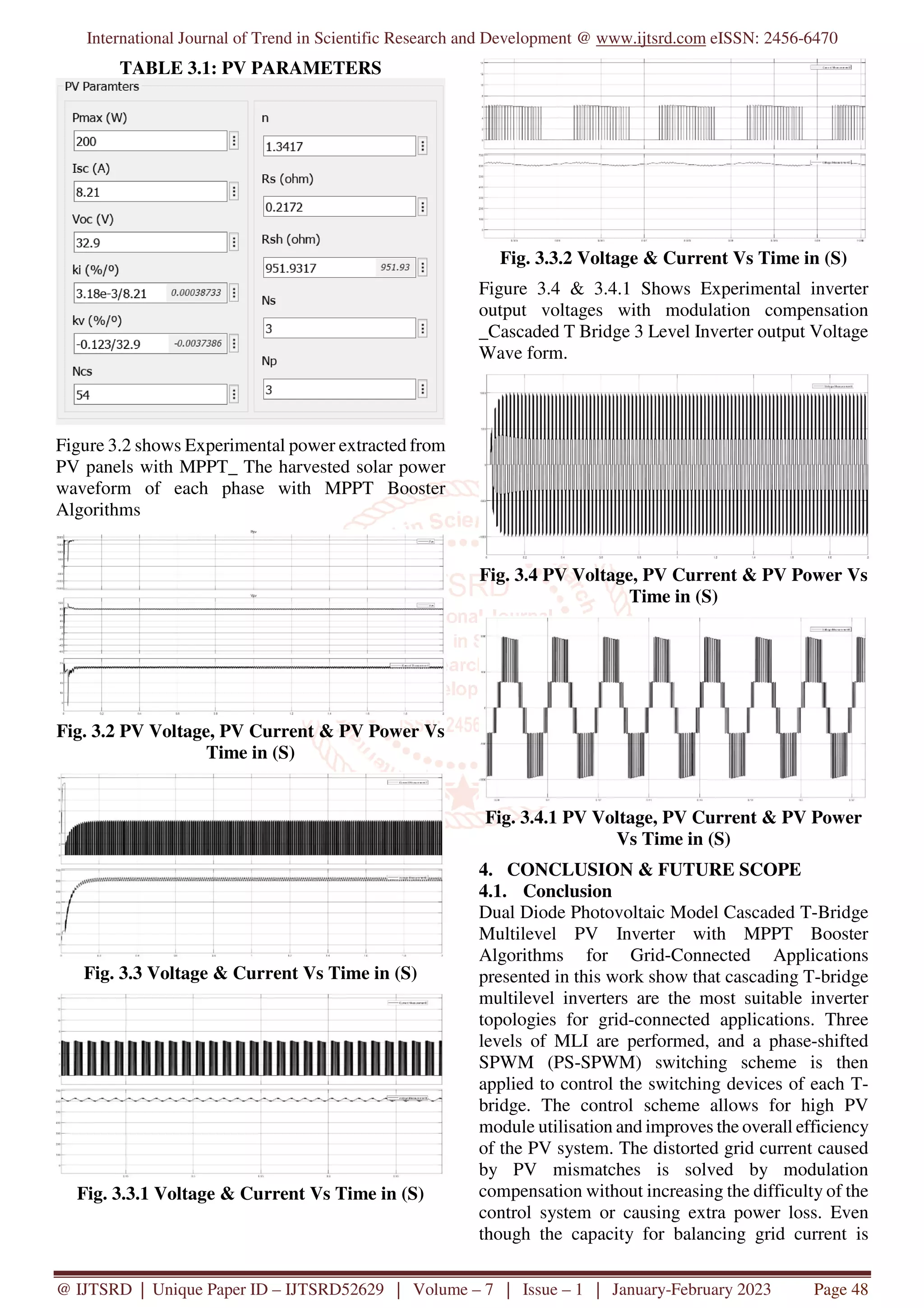
software has been utilized. Table 3.1 shows the
characteristics of the simulated system.
Fig. 3.1 MPPT Algorithms & Cascaded T-bridge
3 Level Inverter](https://image.slidesharecdn.com/8pvtogridconnectedcascadedt-typemultilevelinverterwithimprovedharmonicperformance-230629064753-44aed45d/75/PV-to-Grid-Connected-Cascaded-T-type-Multilevel-Inverter-with-Improved-Harmonic-Performance-11-2048.jpg)
![International Journal of Trend in Scientific Research and Development @ www.ijtsrd.com eISSN: 2456-6470
@ IJTSRD | Unique Paper ID – IJTSRD52629 | Volume – 7 | Issue – 1 | January-February 2023 Page 49
limited, the compensation scheme helps reduce the
percentage of unbalanced grid current. And it also
helps to avoid overmodulation. Hence, the findings
indicate that the CTMLI produces the lowest THD
contents and utilises fewer components. Moreover,
the PS-SPWM produces less THD than SPWM.
4.2. Future Scope
In the proposed multilevel inverter expansion for
3-phase applications, total number of transformers
in the circuit can be reduced by using of cascaded
3-phase transformer circuit instead of single-
phase transformer circuit. In the scheme, total
number of switching components in the circuit is
still a drawback to achieve lower cost and smaller
size of the inverter compared with conventional
multilevel inverter. This is a challenging issue and
new modifications have to be carried out so as to
reduce total switching components.
The proposed inverter has been operated by only
three control schemes, namely Fundamental
switching, SHEPWM and sinusoidal PWM.
Applying the improved switching techniques can
still improve the output quality. So potential of
proposed version could be explored by adopting
different switching techniques.
The proposed version of CMI is only adopted for
active power filter applications. In fact, the merits
of CMI can be used to build for photovoltaic/grid
connected systems. So, it can extend to multiple
applications like STATCOM, SSSC and UPQC
etc.
REFERENCES
[1] Rushikesh Mali; Nitin Adam; Akshay Satpaise;
A. P. Vaidya “Performance Comparison of
Two Level Inverter with Classical Multilevel
Inverter Topologies” 2019 IEEE International
Conference on Electrical, Computer and
Communication Technologies (ICECCT).
[2] Shengwen Fan; Yongji Yu; Yongchang Zhang;
Haitao Yang “Multi-mode Synchronized PWM
Schemes for three-level NPC Inverter” 2019
22nd International Conference on Electrical
Machines and Systems (ICEMS).
[3] V. Anil Kumar; M. Arounassalame
“Comparison of CHB Multi-level inverters
using Level shifted Modulation techniques with
closed loop PI control” 2018 4th International
Conference on Electrical Energy Systems
(ICEES).
[4] Ryosuke Kikuchi; Ryunosuke Araumi; Tomoki
Yokoyama” Deadbeat control for Multi-level
Inverter using 1MHz Multisampling Method
for Utility Interactive System” Ryosuke
Kikuchi; Ryunosuke Araumi; Tomoki
Yokoyama 2018 International Power
Electronics Conference (IPEC-Niigata 2018 -
ECCE Asia).
[5] Gurcharan Singh; Vijay Kumar Garg “THD
analysis of cascaded H-bridge multi-level
inverter” 2017 4th International Conference on
Signal Processing, Computing and Control
(ISPCC).
[6] Sayeeda Farzana; Y. Sumith; K. Ravisankar
“Performance enhancement of three phase
induction motor by using multi-level inverter”
2017 International Conference on Innovative
Mechanisms for Industry Applications
(ICIMIA).
[7] Martin Cheerangal Joy; Jayanand B “Three-
phase infinite level inverter fed induction motor
drive” 2016 IEEE International Conference on
Power Electronics, Drives and Energy Systems
(PEDES).
[8] Ben Bing; Zhang Chunjiang; Guo Zhongnan;
Zhao Xiaojun “Three phase three level inverter
digital control based on over sample and multi-
time calculation” 2016 IEEE 8th International
Power Electronics and Motion Control
Conference (IPEMC-ECCE Asia).
[9] A. Madhukar Rao; N. Kiran Kumar; K.
Sivakumar “A multi-level inverter
configuration for 4n pole induction motor drive
by using conventional two-level inverters”
2015 IEEE International Conference on
Industrial Technology (ICIT).
[10] Abhishek Kumar Ranjan; D. Vijaya Bhaskar;
Nibedita Parida “Analysis and simulation of
cascaded H-bridge multi-level inverter using
level-shift PWM technique” 2015 International
Conference on Circuits, Power and Computing
Technologies [ICCPCT-2015].
[11] Rakesh Kumar Dhal; Tapas Roy “A
comparative study between different multi-
level inverter topologies for different types of
bus clamping PWM techniques using Six
Region Selection Algorithm” Michael Faraday
IET International Summit 2015.
[12] Martin Votava; Tomas Glasberger
“Comparative study of pulse width modulation
techniques for three-level voltage source based
on cascaded connection of two-level inverters”
2015 16th International Scientific Conference
on Electric Power Engineering (EPE).](https://image.slidesharecdn.com/8pvtogridconnectedcascadedt-typemultilevelinverterwithimprovedharmonicperformance-230629064753-44aed45d/75/PV-to-Grid-Connected-Cascaded-T-type-Multilevel-Inverter-with-Improved-Harmonic-Performance-13-2048.jpg)
![International Journal of Trend in Scientific Research and Development @ www.ijtsrd.com eISSN: 2456-6470
@ IJTSRD | Unique Paper ID – IJTSRD52629 | Volume – 7 | Issue – 1 | January-February 2023 Page 50
[13] V Ravi Kumar; A. Sreedevi “Design and
development of Z-source multi-level inverter
for solar energy” 2015 International Conference
on Applied and Theoretical Computing and
Communication Technology (iCATccT).
[14] Saketh Dogga; Sumanth Kumar A. V;
Umasankar S. “A new nine level symmetrical
inverter derived from seven level inverter”
2014 International Conference on Advances in
Electrical Engineering (ICAEE).
[15] Manoj Hirani; Sushma Gupta; D. M.
Deshpande “Comparison of performance of
induction motor fed by sine pulse width
modulated inverter and multi-level inverter
using XILINX” 2014 IEEE International
Conference on Advanced Communications,
Control and Computing Technologies.
[16] Luyao Xie; Jun Qi; Guoqing Weng; Youbing
Zhang “Multi-level PV inverter with
photovoltaic groups independent MPPT
control” 2014 17th International Conference on
Electrical Machines and Systems (ICEMS).
[17] Meher Kalyan U; Sivakumar K “Switching
panels for complete utilisation of battery banks
in multi-level inverters for PV systems” 2014
14th International Conference on Environment
and Electrical Engineering.
[18] Debanjan Roy; Tapas Roy “A new technique to
implement conventional as well as advanced
Pulse Width Modulation techniques for multi-
level inverter” 2014 IEEE 6th India
International Conference on Power Electronics
(IICPE).
[19] Pedram Sotoodeh; Ruth Douglas Miller “A
single-phase 5-level inverter with FACTS
capability using modular multi-level converter
(MMC) topology” 2013 International Electric
Machines & Drives Conference
[20] Abdessattar Guermazi; Karima Halfaoui
“Direct space vector PWM algorithm for
multilevel inverters independent of that of two
levels with neutral point balancing” 10th
International Multi-Conferences on Systems,
Signals & Devices 2013 (SSD13).
[21] Ilhami Colak; Ersan Kabalci; Gokhan Keven
“Comparision of multi-carrier techniques in
seven-level asymmetric cascade multilevel
inverter” 4th International Conference on
Power Engineering, Energy and Electrical
Drives Year: 2013.
[22] Bhanu Naga V Angirekula; Olorunfemi Ojo
“Modeling and analysis of single phase multi
string five level inverter for distributed energy
resources” IECON 2013 - 39th Annual
Conference of the IEEE Industrial Electronics
Society.
[23] Danjiang Chen; Yinzhong Ye; Rong Hua
“Fault diagnosis of three-level inverter based
on wavelet analysis and Bayesian classifier”
2013 25th Chinese Control and Decision
Conference (CCDC).
[24] Masoud Soleimanipour; Hamed Sadeghi
Goughari; Nader Sargolzaei “Analysis and
Comparison of Multi-level Inverters Based on
Two-Level Space Vector PWM” 2012 UKSim
14th International Conference on Computer
Modelling and Simulation.
[25] Musamer Shamil; Mohamed Darwish; Christos
Marouchos “Single phase Multi-level inverter
with desire harmonics” 2012 47th International
Universities Power Engineering Conference
(UPEC).
[26] P. RoshanKumar; P. P. Rajeevan; K. Mathew;
K. Gopakumar; Jose I. Leon; Leopoldo G.
Franquelo “Common-mode voltage eliminated
three-level inverter using a three-level flying-
capacitor inverter and cascaded H-Bridge”
2012 IEEE International Conference on Power
Electronics, Drives and Energy Systems
(PEDES).
[27] G. Preethi; J. Gayathri Monika; V. Jamuna
“Digital simulation of multicarrier PWM
strategy for multi-level inverter” 2012
International Conference on Computing,
Electronics and Electrical Technologies
(ICCEET).
[28] Prasad; A. Sudhakar; Vijay Kumar “Simulation
of five-level inverter fed PMSM based on fast
SVPWM” 2012 IEEE International Conference
on Power Electronics, Drives and Energy
Systems (PEDES).
[29] Ben Slimene Marwa; Khlaifi Mohamed Larbi;
Ben Fredj Mouldi; Rehaoulia Habib “Modeling
and analysis of double stator induction machine
supplied by a multi-level inverter” 2012 16th
IEEE Mediterranean Electrotechnical
Conference.
[30] Dmitry Baimel; Raul Rabinovici; Jacek
Tomasik; Adrian Zuckerberger; Dmitriy Tokar
“Five-level H-bridge inverter fed by multi-
pulse rectifier” 2012 IEEE 27th Convention of
Electrical and Electronics Engineers in Israel.](https://image.slidesharecdn.com/8pvtogridconnectedcascadedt-typemultilevelinverterwithimprovedharmonicperformance-230629064753-44aed45d/75/PV-to-Grid-Connected-Cascaded-T-type-Multilevel-Inverter-with-Improved-Harmonic-Performance-14-2048.jpg)
![International Journal of Trend in Scientific Research and Development @ www.ijtsrd.com eISSN: 2456-6470
@ IJTSRD | Unique Paper ID – IJTSRD52629 | Volume – 7 | Issue – 1 | January-February 2023 Page 51
[31] H. Akagi, H. Fujita, S. Yonetani, and Y.
Kondo, “A 6. 6-kV transformerless STATCOM
b ased on a five-level diode clamped PWM
converter: System design and experimentation
o f a 200-V, 10-kVA laboratory model,” IEEE
Trans. Ind. Appl. , vol. 44, no. 2, pp. 672–680,
Mar. 2008.
[32] Micah Ortúzar, Rodrigo Carmi, Juan Dixon and
Luis Morán, "Voltage-Source Active Power
Filter, Based on Multi-Level Converter and
Ultracapacitor DC Link", IEEE Transactions on
Industrial Electronics, Vol. 53, Nº 2, April
2006, pp. 477- 485.
[33] H. Rudnick, J. Dixon and Luis Morán,
"Delivering Pure and Clean Power", IEEE
Power & Energy Magazine, Vol. 1, Nº 5,
September/October 2003, pp32-40.
[34] Ogasawara, S., and Akagi, H.: ‘Analysis of
variation of neutral point potential in neutral-
point-clamped voltage source PWM inverters’.
Conf. Rec. IEEE-IAS Annual Meeting,
Toronto, Canada, 1993, pp. 965–970.
[35] ÇolakI, Kabalci E. The control methods of
multi-level inverter. TUBAV Sci 2009; 1: 45–
54.
[36] Jouanne, A. V., Dai, S., and Zhang, H.: ‘A
multilevel inverter approach providing DC- link
balancing, ride-through enhancement, and
common-mode voltage elimination’, IEEE
Trans. Ind. Electron., 2002, 49, pp. 739–745
[37] W. McMurray, “Fast response stepped-wave
switching power converter circuit,” U. S. Patent
3 581 212, May 25, 1971.
[38] J. A. Dickerson and G. H. Ottaway,
“Transformerless power supply with line to
load isolation,” U. S. Patent 3 596 369, Aug. 3,
1971.
[39] P. M. Bhagwat and V. R. Stefanovic,
“Generalized structure of a multilevel PWM
inverter,” IEEE Trans. Ind. Applicat., vol. 19,
no 6, pp. 1057-1069, Nov. /Dec. 1983.
[40] R. H. Baker, “Bridge converter circuit,” U. S.
Patent 4 270 163, May 26, 1981.
[41] Celanovic, N., and Boroyevich, D.: ‘A
comprehensive study of neutralpoint voltage
balancing problem in three-lever neutral-point
clamped voltage source PWM inverters’, IEEE
Trans. Power Electron., 2000, 15, pp. 242–249.
[42] Lee, Y. H., Kim, R. Y., and Hyum, D. S.: ‘A
novel SVPWM strategy considering dc-link
balancing for a multi-level voltage source
inverter’. Proc. IEEE APEC, Dallas, USA,
1999, pp. 509–514.
[43] M. Marchesoni, M. Mazzucchelli, and S.
Tenconi, “A non-conventional power converter
for plasma stabilization,” in Proc. IEEE 19th
Power Electron. Spec. Conf., Apr. 11–14, 1988,
pp. 122–129.
[44] P. W. Hammond, “A new approach to enhance
power quality for medium voltage drives,” in
Proc. Ind. Appl. Soc. 42nd Annu. Petroleum
Chem. Ind. Conf., Sep. 11–13, 1995, pp. 231–
235.
[45] Ryszard Strzelecki, Grzegorz Benysek, “Power
electronics in smart electrical energy
networks,” Springer-ISBN 978-1-84800-317-0,
2008.
[46] Z. Peng, “A generalized multilevel i nverter
topology with self-voltage balancing,” IEEE
Trans. Ind. Applicat., vol. 37, March/April
2001, pp. 611–618,.
[47] K. Corzine and Y. Familiant, “A new cascaded
multilevel H-bridge drive,” IEEE Trans. Power
Electron. , vol. 17, no. 1, pp. 125–131, Jan.
2002.
[48] P. McGrath and D. G. Holmes, “Natural
capacitor voltage balancing for a flying
capacitor converter induction motor drive,”
IEEE Trans. Power Electron. , vol. 24, no. 6,
pp. 1554–1561, Jun. 2009.
[49] M. Hagiwara, K. Nishimura, and H. Akagi, “A
medium-voltage motor drive with a modular
multilevel PWM inverter,” IEEE Trans. Power
Electron, vol. 25, no. 7, pp. 1786–1799, Jul.
2010.
[50] J. Wang and F. Z. Peng, “Unified power flow
controller using the cascade multilevel
inverter,” IEEE Trans. Power Electron, vol. 19,
no. 4, pp. 1077–1084, Jul. 2004.
[51] Q. Song and W. Liu, “Control of a cascade
STATCOM with star con-figuration under
unbalanced conditions,” IEEE Trans. Power
Electron. , vol. 24, no. 1, pp. 45–58, Jan. 2009.
[52] J. Zaragoza, J. Pou, S. Ceballos, E. Robles, C.
Jaen, and M. Corbalan, “Voltage-balance
compensator for a carrier-based modulation in
the neutral-point-clamped converter,” IEEE
Trans. lnd. Electron., vol. 56, pp. 305–314, Feb.
2009.](https://image.slidesharecdn.com/8pvtogridconnectedcascadedt-typemultilevelinverterwithimprovedharmonicperformance-230629064753-44aed45d/75/PV-to-Grid-Connected-Cascaded-T-type-Multilevel-Inverter-with-Improved-Harmonic-Performance-15-2048.jpg)
![International Journal of Trend in Scientific Research and Development @ www.ijtsrd.com eISSN: 2456-6470
@ IJTSRD | Unique Paper ID – IJTSRD52629 | Volume – 7 | Issue – 1 | January-February 2023 Page 52
[53] Okayama, R. Uchida, M. Koyama, S.
Mizoguchi, S. Tamai, H. Ogawa, T. Fujii, Y.
Shimomura, “Large capacity high performance
3-level GTO inverter system for steel main
rolling mill drives,” in Conf. Rec. IAS Annu.
Meeting , 1996, pp. 174–179.
[54] S. Bernert, “Recent developments of high
power converters for industry and traction
applications,” IEEE Trans. Power Electron. ,
vol. 15, no. 6, pp. 1102–1117, Nov. 2000.
[55] S. Alepuz, S. Busquets-Monge, J. Bordonau, J.
Gago, D. Gonzalez, and J. Balcells,
“Interfacing renewable energy sources to the
utility grid us-ing a three-level inverter,” IEEE
Trans. Ind. Electron., vol. 53, no. 5, pp. 1504–
1511, Oct. 2006.
[56] Y. Cheng, C. Qian, M. L. Crow, S. Pekarek,
and S. Atcitty, “A comparison of diode-
clamped and cascaded multilevel converters for
a STATCOM with energy storage,” IEEE
Trans. Ind. Electron. , vol. 53, no. 5, pp. 1512–
1521, Oct. 2006.
[57] P. K. Steimer, H. E. Gruning, J. Werninger , E.
Carroll, S. Klaka, S. Linder “IGCT—A new
emerging technology for high power, low cost
inverters,” IEEE Ind. Appl. Mag. , vol. 5, no. 4,
pp. 12–18, Jul. /Aug. 1999.
[58] Brunner, M. Hieholzer, T. Laska, A. Porst,
“Progress in development of the 3. 5 kV high
voltage IGBT/diode chipset and 1200 A
module applications,” in Proc. IEEE Int. Symp.
Power Semicond. Devices IC’s, 1997, pp. 225–
228.
[59] B. Wu, High-Power Converters and AC Drives.
New York: Wiley-IEEE Press, Mar. 2006.
[60] N. S. Choi, J. G. Cho and G. H. Cho, “A
general circuit topology of multilevel inverter,”
in Proc. IEEE-PESC, 1991, pp. 96-103.](https://image.slidesharecdn.com/8pvtogridconnectedcascadedt-typemultilevelinverterwithimprovedharmonicperformance-230629064753-44aed45d/75/PV-to-Grid-Connected-Cascaded-T-type-Multilevel-Inverter-with-Improved-Harmonic-Performance-16-2048.jpg)