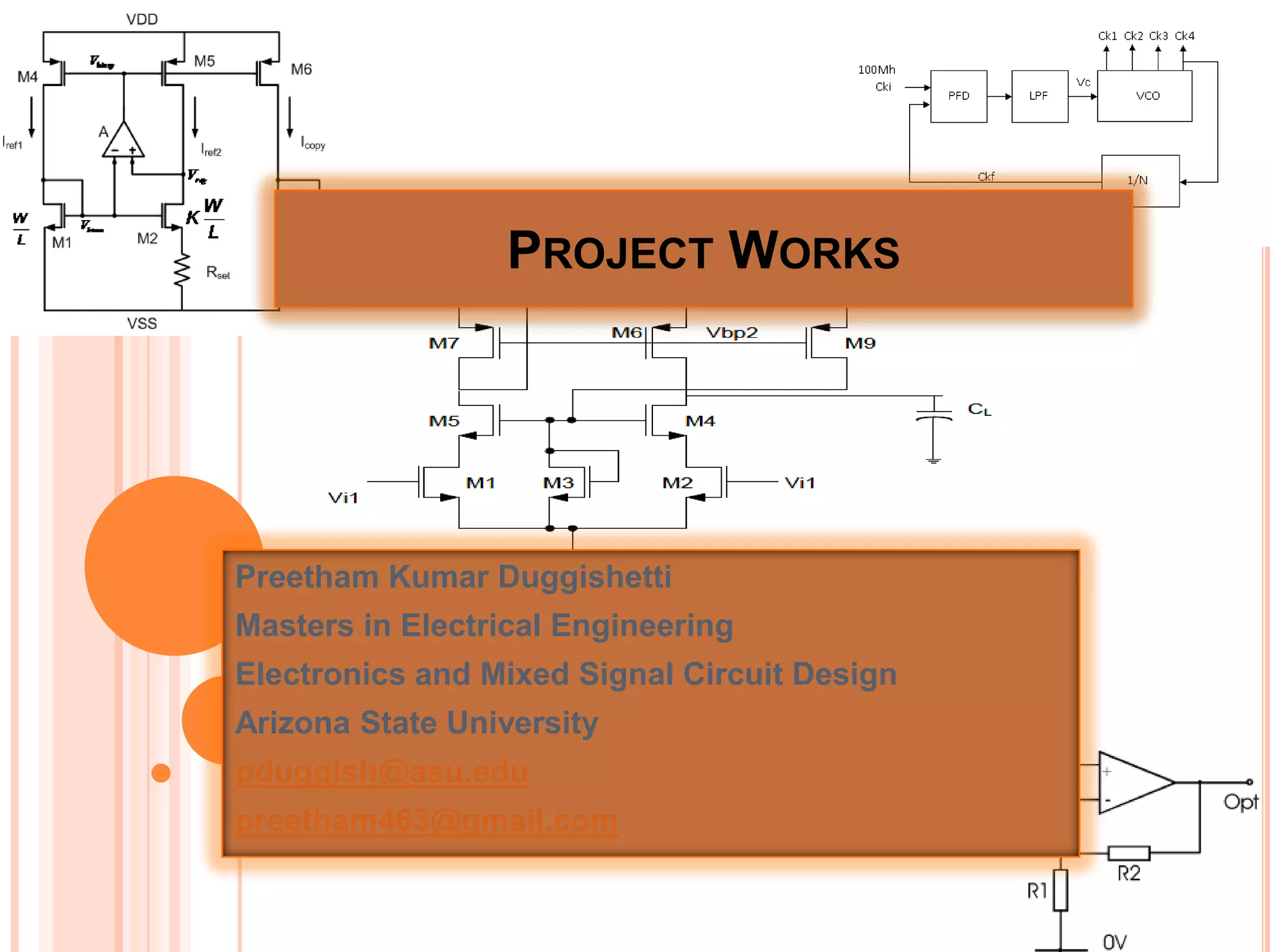
Project Works Preetham Kumar DuggishettiMasters in Electrical EngineeringElectronics and Mixed Signal Circuit DesignArizona State Universitypduggish@asu.edupreetham463@gmail.com
 PHASE LOCKED LOOP 	0.18 um technology
Cadence (Spectre ) , VerilogA, MATLAB.
Generated 4 equally spaced clocks at 1.6GHz with CMOS full-swing (1.8V), achieved 300ns lock time for 1.6GHz oscillation.
A maximum jitter of ±82ps was obtained, the PLL consumed 4.87mW when locked. A Behavioral model for the PLL using Verilog A, MATLAB was developed. Design of LOW POWER HIGH SPEED 32 BIT ALU 	0.25um technology
Cadence (Spectre, Virtuso)
Requirement : Power consumption to be least with a delay constraint of 10 nS, output transition time lower than 200pS with a load of 30 fF at the -10%Vdd and Slow-Slow Design corner.
Understood various design techniques for Low Power and procedures to choose the right logic style.
Layout  done using Virtuoso & power was 8.65 pJ without layout parasitic and 16 pJ with  parasitics.STURDY MASH 2-1 MODULATOR FOR WLAN SYSTEMS(Oversampling Sigma Delta ADC)0.35 um technology

Projects

  • 1.
    Project Works PreethamKumar DuggishettiMasters in Electrical EngineeringElectronics and Mixed Signal Circuit DesignArizona State Universitypduggish@asu.edupreetham463@gmail.com
  • 2.
    PHASE LOCKEDLOOP 0.18 um technology
  • 3.
    Cadence (Spectre ), VerilogA, MATLAB.
  • 4.
    Generated 4 equallyspaced clocks at 1.6GHz with CMOS full-swing (1.8V), achieved 300ns lock time for 1.6GHz oscillation.
  • 5.
    A maximum jitterof ±82ps was obtained, the PLL consumed 4.87mW when locked. A Behavioral model for the PLL using Verilog A, MATLAB was developed. Design of LOW POWER HIGH SPEED 32 BIT ALU 0.25um technology
  • 6.
  • 7.
    Requirement : Powerconsumption to be least with a delay constraint of 10 nS, output transition time lower than 200pS with a load of 30 fF at the -10%Vdd and Slow-Slow Design corner.
  • 8.
    Understood various designtechniques for Low Power and procedures to choose the right logic style.
  • 9.
    Layout doneusing Virtuoso & power was 8.65 pJ without layout parasitic and 16 pJ with parasitics.STURDY MASH 2-1 MODULATOR FOR WLAN SYSTEMS(Oversampling Sigma Delta ADC)0.35 um technology
  • 10.
    Cadence (Spectre ), MATLAB/SIMULINK, VerilogA .
  • 11.
    10MHZ signal bandwidth,50dB Input dynamic range. Complete transistor level circuit implementation and Behavioral model using Simulink/Matlab and VerilogA.TELESCOPIC CASCODE DIFFERENTIAL AMPLIFIER & biasing 0.35 um technology
  • 12.
  • 13.
    Dc gain >50dB, Ft = 70MHz with CL = 1pF, Tail current source < 110uA.
  • 14.
    Understood Test benchsetups for CMRR, PSRR+, PSRR-, Slew Rate configurationsCMOS β MULTIPLIER BASED CONSTANTgm CURRENT REFERENCE0.35 um technology
  • 15.
  • 16.
    Understood IC biasingcircuits and their variations with supply and temperature.
  • 17.
    Optimized transistorsizes and generated equal currents over a wide range of Vdd. DESIGN OF A SINGLE ENDED FOLDED CASCODE AMPLIFIER0.35 um technology
  • 18.
    Cadence (Spectre ,Virtuso Layout Editor )
  • 19.
    High gain, UGFof 25 MHz with 15pF capacitive load, input referred noise of 10nV/sqHz, Quiescent Power dissipation of 1.2mW, Slew rate of 10V/usec with 5pF cap load, PSRR and CMRR of 55dB at 10 KHz and Phase margin of 60 degrees with 5pF capacitive load.
  • 20.
    Also Done theLayout using various Analog design techniques.IBM CELL Processor ProgrammingImprovised the performance of an FFT algorithm on IBM CELL Processor by using multithreading concept (scheduled for implementation by IBM in near future)Design of a PROGRAMMABLE SIGMA DELTA ANALOG TO DIGITAL CONVERTERModulator had to be programmable to be used in a single chip receiver supporting both cellular (GSM) as well as cordless (DECT) phones.
  • 21.
    Matlab/Simulink tools wereused and a resolution of 14 bit and 12 bit respectively were achieved.