This document discusses the practical uses of surface mount adhesives in printed circuit board assemblies. It covers topics such as:
- The role of adhesives in holding components during wave soldering
- Factors to consider when selecting nozzles for adhesive dispensing like pad spacing, dot size, and standoff distance
- Relationships between nozzle diameter, standoff distance, and dispensed dot size and shape
- Applications that require special nozzle designs like dispensing adhesive between solder paste screened pads
- Process parameters like cure profiles and temperatures for different applications
The rapid assimilation of Ball Grid Array (BGA) and other
Area Array Package technology in the electronics industry
is due to the fact that this package type allows for a greater I/O count in a smaller area while maintaining a pitch that allows for ease of manufacture.
RELONG concentrates on developing, manufacturing and supplying advanced printed circuit board laminate material for high frequency and microwave applications. RELONG offers a broad range of low Dk, low loss PTFE laminate and Hydrocarbon prepreg products to satisfy customer’s ever-challenging performance and cost requirements.
Elcometer 138 Bresle Salt Kit to level of contaminants on a surface is measur...MM Naina Exports
Multilab Supplies, Distributes and Imports Elcometer 138 Bresle Salt Kit to level of contaminants on a surface is measured prior to application of the coating to ensure the quality of the coating and that its optimum lifetime is achieved
http://www.multilab.biz/testing/elcometer-testing-equipments/surface-cleanliness/elcometer138-bresle-salt-kit.htm
Product Description
It is essential that the level of contaminants on a surface is measured prior to application of the coating to ensure the quality of the coating and that its optimum lifetime is achieved.
If the coating is applied to a contaminated surface, which is not properly prepared, it could fail prematurely resulting in costly re-coating and high maintenance costs.
The Elcometer 138 Bresle Kit includes the Elcometer 138 Conductivity Meter. This lightweight, portable conductivity meter accurately measures the salinity of the test samples.
The cartridge type sensor can be easily replaced when necessary and displays conductivity (µS/cm and mS/cm) and salinity (%) on the digital display.
Features of the meter include indication of stability of reading indication.
(https://www.indiamart.com/swatienterprise) We “Swati Enterprise” are a Sole Proprietorship firm engaged in manufacturing high-quality array of Brass Bush, Brass Washer, Brass Screw, etc.
A Silicon-to-System Thermo-Mechanical Review of ElectronicsKamal Karimanal
A Silicon-to-System Review of Thermo-Mechanical Considerations in Electronics
Author: Kamal Karimanal, Cielution LLC
Thermal and Mechanical challenges to IC package reliability has been addressed with a sufficiently working system of information exchange across a supply chain that spans the foundries to system level assembly plants.The never ending market demand for miniaturization, performance, functionality and cost reduction invariably translates to manufacturing, design, assembly, and reliability challenges to the engineer. Within the Thermal and Mechanical realm these challenges manifest to the engineer in the form of seemingly disconnected problems areas such as BEOL yield, flipchip interconnect reliability, warpage mitigation, heat sink retention design, interface choice, thermally aware board and chassis layout, fan sizing and system level optimization. Evolving technology also introduces newer puzzles such as heterogeneous packaging using 3D ICs. The talk will focus on the tools, methodologies and information exchange protocols used by the thermal management and mechanical reliability professionals across the supply chain to address the various challenges.
The objective of any rework process is to duplicate as closely as possible the original manufacturing
process while not disturbing neighboring components while still meeting the original specifications and
assembly criteria of the PCB .
This paper will present a rigorous method for evaluating the performance and economic benefits of solder paste stencil nano-coatings. Criterion such as underside cleaning, bridging, transfer efficiency across SARs, solder paste deposit geometry, post-print cleaning, and abrasion resistance of the coating, will all be considered and weighted. Performance of currently available coatings will be compared. A discussion of the economic impact on current and future SMT design will be included.
SPIROL Spring Alignment Dowels and Bushings CatalogSPIROL
SPIROL roll-formed, hardened Spring Dowels and Dowel Bushings are designed to align mating components, eliminate drilling of a separate bolt hole, protect bolts from shear loading, and/or maintain joint integrity. The 12-page design guide provides product specification data and pages of helpful design guidelines. Four pages of applications are included.
My name is Elena Long. I am associated with matlabassignmentexperts.com as an Matlab Assignment help expert for the past 4 years and have been helping students with their assignments. I have a Ph.D. in Mechanical Engineering, from McGill University, Canada.
COLLEGE BUS MANAGEMENT SYSTEM PROJECT REPORT.pdfKamal Acharya
The College Bus Management system is completely developed by Visual Basic .NET Version. The application is connect with most secured database language MS SQL Server. The application is develop by using best combination of front-end and back-end languages. The application is totally design like flat user interface. This flat user interface is more attractive user interface in 2017. The application is gives more important to the system functionality. The application is to manage the student’s details, driver’s details, bus details, bus route details, bus fees details and more. The application has only one unit for admin. The admin can manage the entire application. The admin can login into the application by using username and password of the admin. The application is develop for big and small colleges. It is more user friendly for non-computer person. Even they can easily learn how to manage the application within hours. The application is more secure by the admin. The system will give an effective output for the VB.Net and SQL Server given as input to the system. The compiled java program given as input to the system, after scanning the program will generate different reports. The application generates the report for users. The admin can view and download the report of the data. The application deliver the excel format reports. Because, excel formatted reports is very easy to understand the income and expense of the college bus. This application is mainly develop for windows operating system users. In 2017, 73% of people enterprises are using windows operating system. So the application will easily install for all the windows operating system users. The application-developed size is very low. The application consumes very low space in disk. Therefore, the user can allocate very minimum local disk space for this application.
Sachpazis:Terzaghi Bearing Capacity Estimation in simple terms with Calculati...Dr.Costas Sachpazis
Terzaghi's soil bearing capacity theory, developed by Karl Terzaghi, is a fundamental principle in geotechnical engineering used to determine the bearing capacity of shallow foundations. This theory provides a method to calculate the ultimate bearing capacity of soil, which is the maximum load per unit area that the soil can support without undergoing shear failure. The Calculation HTML Code included.
Courier management system project report.pdfKamal Acharya
It is now-a-days very important for the people to send or receive articles like imported furniture, electronic items, gifts, business goods and the like. People depend vastly on different transport systems which mostly use the manual way of receiving and delivering the articles. There is no way to track the articles till they are received and there is no way to let the customer know what happened in transit, once he booked some articles. In such a situation, we need a system which completely computerizes the cargo activities including time to time tracking of the articles sent. This need is fulfilled by Courier Management System software which is online software for the cargo management people that enables them to receive the goods from a source and send them to a required destination and track their status from time to time.
CFD Simulation of By-pass Flow in a HRSG module by R&R Consult.pptxR&R Consult
CFD analysis is incredibly effective at solving mysteries and improving the performance of complex systems!
Here's a great example: At a large natural gas-fired power plant, where they use waste heat to generate steam and energy, they were puzzled that their boiler wasn't producing as much steam as expected.
R&R and Tetra Engineering Group Inc. were asked to solve the issue with reduced steam production.
An inspection had shown that a significant amount of hot flue gas was bypassing the boiler tubes, where the heat was supposed to be transferred.
R&R Consult conducted a CFD analysis, which revealed that 6.3% of the flue gas was bypassing the boiler tubes without transferring heat. The analysis also showed that the flue gas was instead being directed along the sides of the boiler and between the modules that were supposed to capture the heat. This was the cause of the reduced performance.
Based on our results, Tetra Engineering installed covering plates to reduce the bypass flow. This improved the boiler's performance and increased electricity production.
It is always satisfying when we can help solve complex challenges like this. Do your systems also need a check-up or optimization? Give us a call!
Work done in cooperation with James Malloy and David Moelling from Tetra Engineering.
More examples of our work https://www.r-r-consult.dk/en/cases-en/
Event Management System Vb Net Project Report.pdfKamal Acharya
In present era, the scopes of information technology growing with a very fast .We do not see any are untouched from this industry. The scope of information technology has become wider includes: Business and industry. Household Business, Communication, Education, Entertainment, Science, Medicine, Engineering, Distance Learning, Weather Forecasting. Carrier Searching and so on.
My project named “Event Management System” is software that store and maintained all events coordinated in college. It also helpful to print related reports. My project will help to record the events coordinated by faculties with their Name, Event subject, date & details in an efficient & effective ways.
In my system we have to make a system by which a user can record all events coordinated by a particular faculty. In our proposed system some more featured are added which differs it from the existing system such as security.
Quality defects in TMT Bars, Possible causes and Potential Solutions.PrashantGoswami42
Maintaining high-quality standards in the production of TMT bars is crucial for ensuring structural integrity in construction. Addressing common defects through careful monitoring, standardized processes, and advanced technology can significantly improve the quality of TMT bars. Continuous training and adherence to quality control measures will also play a pivotal role in minimizing these defects.
Hybrid optimization of pumped hydro system and solar- Engr. Abdul-Azeez.pdffxintegritypublishin
Advancements in technology unveil a myriad of electrical and electronic breakthroughs geared towards efficiently harnessing limited resources to meet human energy demands. The optimization of hybrid solar PV panels and pumped hydro energy supply systems plays a pivotal role in utilizing natural resources effectively. This initiative not only benefits humanity but also fosters environmental sustainability. The study investigated the design optimization of these hybrid systems, focusing on understanding solar radiation patterns, identifying geographical influences on solar radiation, formulating a mathematical model for system optimization, and determining the optimal configuration of PV panels and pumped hydro storage. Through a comparative analysis approach and eight weeks of data collection, the study addressed key research questions related to solar radiation patterns and optimal system design. The findings highlighted regions with heightened solar radiation levels, showcasing substantial potential for power generation and emphasizing the system's efficiency. Optimizing system design significantly boosted power generation, promoted renewable energy utilization, and enhanced energy storage capacity. The study underscored the benefits of optimizing hybrid solar PV panels and pumped hydro energy supply systems for sustainable energy usage. Optimizing the design of solar PV panels and pumped hydro energy supply systems as examined across diverse climatic conditions in a developing country, not only enhances power generation but also improves the integration of renewable energy sources and boosts energy storage capacities, particularly beneficial for less economically prosperous regions. Additionally, the study provides valuable insights for advancing energy research in economically viable areas. Recommendations included conducting site-specific assessments, utilizing advanced modeling tools, implementing regular maintenance protocols, and enhancing communication among system components.
Forklift Classes Overview by Intella PartsIntella Parts
Discover the different forklift classes and their specific applications. Learn how to choose the right forklift for your needs to ensure safety, efficiency, and compliance in your operations.
For more technical information, visit our website https://intellaparts.com
Democratizing Fuzzing at Scale by Abhishek Aryaabh.arya
Presented at NUS: Fuzzing and Software Security Summer School 2024
This keynote talks about the democratization of fuzzing at scale, highlighting the collaboration between open source communities, academia, and industry to advance the field of fuzzing. It delves into the history of fuzzing, the development of scalable fuzzing platforms, and the empowerment of community-driven research. The talk will further discuss recent advancements leveraging AI/ML and offer insights into the future evolution of the fuzzing landscape.
Explore the innovative world of trenchless pipe repair with our comprehensive guide, "The Benefits and Techniques of Trenchless Pipe Repair." This document delves into the modern methods of repairing underground pipes without the need for extensive excavation, highlighting the numerous advantages and the latest techniques used in the industry.
Learn about the cost savings, reduced environmental impact, and minimal disruption associated with trenchless technology. Discover detailed explanations of popular techniques such as pipe bursting, cured-in-place pipe (CIPP) lining, and directional drilling. Understand how these methods can be applied to various types of infrastructure, from residential plumbing to large-scale municipal systems.
Ideal for homeowners, contractors, engineers, and anyone interested in modern plumbing solutions, this guide provides valuable insights into why trenchless pipe repair is becoming the preferred choice for pipe rehabilitation. Stay informed about the latest advancements and best practices in the field.
The Benefits and Techniques of Trenchless Pipe Repair.pdf
Practical production uses_of_smt_adhesives
1. PRACTICAL PRODUCTION USES OF SMT ADHESIVES
By Steven Rocco Marongelli, Douglas Dixon,
Sergio Porcari, Wendy Cummings,
Frank Murch, Al Osterhout
Universal Instruments
GDM Product Team
PO Box 825
Binghamton, NY USA
13902-0825
607-779-1134
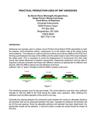
Introduction
Adhesives are typically used in surface mount Printed Circuit Board (PCB) assemblies to hold
the passive, (and sometimes active), components on to the bottom side of the board during
wave soldering. The adhesive is used to bond the surface mount device (SMD) to the PCB, thus
forming a joint between the body of the (SMD) and the solder resist or bare FR-4 board between
the solder pads. This is necessary to avoid the displacement of components from their sites
during high speed placement of passive components. Dispensing equipment must be able to
dispense a precise consistent dot shape with different volumes as appropriate for different size
devices. After the SMD is placed, the wet adhesive must have
sufficient “wet” or “green” strength to hold the SMD in position until cured.
Figure 1
The hardening process must be fast and simple. The cured adhesive must then have sufficient
strength to hold the SMD to the PCB during the solder wave operation. After soldering the
adhesive must not affect operation of the circuit in any way.
Generally the spacing between the component pads dictates the maximum allowable adhesive
dot diameter that can be dispensed between the pads. Typically the adhesive dot diameter will
be 2/3 the pad spacing. Once the allowable adhesive dot diameter has been determined, the
appropriate nozzle can be selected. A dual dot nozzle or single dot nozzle should be chosen at
this time.
PCB
Acceptable
PCB PCB
Unacceptable
Pad Contamination
Unacceptable
Component Bond Area
Sufficient
Component Bond Area
Insufficient
2. Why Dual Dots
From time to time the question comes up about why dual
dots are sometimes used and sometimes not. The reasons
are very logical but rarely stated. Adhesive adheres to a
surface in a way that is directly proportional to its area. The
amount of adhesive one can put under a component with a
single dot is shown in figure 2. This assumes a 3 mil stand
off and pad widths matching the component. The mass of
each of these common components is also shown in figure 3.
The 0805 and larger components are thicker and therefore
have more mass. The amount of adhesion area required
increases because of the increase in mass. However the
space under the component is limited. The Figure 2
relationship between mass and area is shown in figure 3.
The 0805 component is the breaking point where the
advantage of using dual dots exists but is not strong. The
components larger than 0805s require dual dots. In
addition to the increased mass these larger components
have higher centers of gravity due to the increased
thickness. Naturally, the exact point where the area and
the green or cured strength balance, depends on the
specific adhesive and the G forces of the chip shooter.
Nozzle Selection
Choosing a nozzle for use in dispensing adhesives requires knowledge of what dot size is
required. The dot size requirements can be derived from the board design being utilized or
specifically the pad spacing of components. It is not uncommon for Manufacturing Engineer
personnel or Quality Engineering personnel of a printed circuit board manufacturing facility, to
inquire what a recommended adhesive dot diameter should be for a particular component type.
Much has been written in regards to recommended surface mount component pad designs and
layouts for bottom side applications. (“Wave Solder”) Top side pad designs are used on bottom
side PCB fabrication. However these guidelines are rarely utilized. The pad spacing for a
particular component for each individual customer product is unique. Universal’s surface mount
laboratory, has recommended component pad spacing guidelines for use when designing
printed circuit boards for adhesive application.
0402
(1005)
0603
(1608)
0805
(2012)
1206
(3216)
1210
(3225)
Dual Dot Advantage
0
50
100
150
200
0402 0603 0805 1206 1210
Ratio
of
Force
to
Area
Single Dot
Single Dot
Dual Dot
3. 0402 0603 0805 1206 1210
A 0.013" 0.020" 0.035" 0.040" 0.060"
B 0.025" 0.040" 0.040" 0.070" 0.070"
C 0.121" 0.140" 0.140" 0.205" 0.205"
D1 0.010"-0.015" 0.020"-0.025"
D2 0.020"-0.035" 0.020"-0.035" 0.020"-0.035"
E 0.035" 0.035" 0.035"
A
C
B
D1
E
Recommended Contact Pattern Footprint D2
Table 1
Because the pad spacing for most typical surface mount components is not standardized from
one customer product to another, it becomes a challenging task when recommending what
tooling should be utilized to satisfy a particular customers adhesive deposition requirement for a
particular component.
Typically, surface mount component pads for a particular circuit board are designed for either
adhesive deposition or screening of solderpaste. (See Figure 4) The pad spacing is generally
smaller for solderpaste application as opposed to that of adhesive deposition. For example, the
component pad spacing between the pads of an 0603 chip cap/resistor is typically 0.020” if the
board was designed to be screen printed with solderpaste. The pad spacing for the same board
can be 0.040” if adhesive deposition was intended to be utilized.
A 0.030” diameter dot of
adhesive would easily be
recommended for use if the
component pads on the board
were indeed designed for
adhesive deposition. However, if
the pad design for the same
board was originally designed
for utilization of solderpaste, as
a method of adhering the
component to the board,
obviously
an 0.030” diameter dot of adhesive Figure 4
would be too large, as the spacing
between the pads is now 0.020”. A
0.040"
0.030"
0603
0603
Typical Wave Solder Pad Layout For
0603 Chip Component
Typical Solder Paste Pad Layout For
0603 Chip Component
0603
0603
Typically 0.015" - 0.020"
Typically 0.018" - 0.025"
4. 0.015” to 0.018” diameter dot is required for this particular application.
Therefore, because all pad design and spacing is not the same from one circuit board to another
the actual spacing between the pads of the particular component must be known.
Note that the volume of adhesive needed to maintain the component in place during the high
speed placement or wave solder process may be larger than possible for some specific pad
designs. Nozzle selection refers in this case to specific nozzle specifications for a known dot
size requirement.
When selecting a nozzle for use in dispensing adhesives,
the main parameters needed for correctly determining
correct nozzle selection are Nozzle ID, Nozzle Stand-Off,
and Dot Diameter. The nozzle standoff can be defined as
the distance from the tip of the dispensing surface to the
end of the mechanical standoff. The nozzle standoff is used
to maintain the distance between the PCB and the
dispensing tip. Most dispensers in use today are designed
to utilize some sort of mechanical standoff with Figure 5
the nozzles.
The stand-off usually dictates, to some degree, the height of the dispensed dot. If the stand-off is
too large the adhesive may never contact the board. If this condition exists than the adhesive will
build up on the bottom side of the nozzle. Generally this condition leads to poor dot shapes,
inconsistent volume, stringing and missing dots.
Relationship Of Adhesive Dot Height To Component Height From the Board
The distance between the bottom of the component and the top of the PC board is typically
between 0.003” to 0.005”. In order to assure a good bond or wetting of the adhesive to the
bottom of the component as it is placed onto the PC board, a good rule of thumb is to utilize a
dot height that is twice the distance between the bottom of the component and the top of the PC
board.
Stand Off
Noz
I.D.
PCB
5. Figure 6
Table 2
From table 2 above it can be derived that as the nozzle ID and nozzle standoff decrease the dot
diameter range also diminishes. It can also be noted that the recommended standoff for the 8
mil ID nozzle is the same as the 10 mil nozzle. It is recommended not to to go below the 5 mil
standoff due to tolerancing of PCB fabrication. Dot diameters smaller than that of a 16 mil dot
require special care from board manufacturing. Slight variations of pad heights and solder mask
on the PCB add up to large variations in actual mechanical standoff while dispensing. When
dispensing dots that require going through nozzles of 8 mils or less the adhesives used and the
particle size within the adhesives. Small nozzle ID’s with large particle size will tend to clog more
often making for a less than robust manufacturing process.
PCB
Component
Pad
Adhesive Solder Resist
A
2 X A
PCB
Component
Pad
Solder Resist
Adhesive Solder Resist
Typically 0.003" to 0.005"
Nozzle ID Nozzle Standoff Dot Diameter Range Optimal Dot Diameter
8 5 16-20 18
10 5 18-22 20
12 8 24-35 28
16 10 28-45 35
23 15 40-60+ 45
33 20 50-100+ 60
6. Figure 7
DOT DIA
Noz
I.D.
Stand
Off Note:
Adhesive dot diameter is approximately 2X
the Inside
Diameter of the nozzle.
Surface Tension of adhesive @ PC Board is 2X area in relationship to inside diameter of nozzle.
Final result is repetition of well defined dot of constant volume.
CorrectRelationship Between Nozzle I.D./ Nozzle Stand-Off/
Adhesive Dot Diameter
Correct adhesive volume dispensed.
DOT DIA
Stand
Off
Noz
I.D.
Note:
Adhesive dot diameter is exceeds the recommended 2X
Nozzle I.D.. Excessive adhesive is forced to migrate
throughout the inside of the outer nozzle stand-off.
IncorrectRelationship Between Nozzle I.D./ Nozzle Stand-Off/
Adhesive Dot Diameter
Incorrectadhesive volume dispensed.
Surface Tension of adhesive @ PC Board is less than the recommended 2X nozzle I.D.
The surface tension of the adhesive @ the nozzle now exceeds that of the board, due to large amount of adhesive build-up inside
nozzle bore. The snap off therefore is inconsistent.
Final result is inconsistent dot volume and poor dot shape. A pattern of large dot, small dot may develop. This occurs because @ every
other dispense there is almost twice the amount of dispensed adhesive @ the nozzle tip.
Stroke
Stroke
Stroke
Stroke
Stroke
This excessive
amount of adhesive
will be added to the
next dispensed dot.
7. Figure 8
Figure 9
Nozzle Tolerancing and Wear
Since the dot diameter is integrally tied to the nozzle ID and the nozzle standoff, nozzles will vary
slightly in performance due to nozzle tolerancing and nozzle wear. With the repeated force of the
nozzle standoff hitting the PCB the mechanical standoff will wear. The amount of wear seen on
the nozzle depends on the type of solder mask used on the PCB and the type of metal used in
the nozzle construction. It is important to monitor this wear so that the nozzle performance is
optimal. A reduced mechanical standoff will result in a smaller dot diameter range capability.
Low standoffs limit the size of the large dots. As the standoff wears down the adhesive will
contaminate the dispensing tip.
DOTDIA
Stand
Off
Noz
I.D.
Note:
Adhesive dot diameter is smaller than the recommended 2X
Nozzle I.D.. Not enough adhesive will contact the PC board.
Incorrect Relationship Between Nozzle I.D./ Nozzle Stand-Off/
Adhesive Dot Diameter
Incorrect adhesive volume dispensed.
Stroke
Stroke
Stroke
Stroke
Stroke
Surface Tension of adhesive @ PC Board is less than the recommended 2X nozzle I.D..
The surface tension of the adhesive @ the nozzle now exceeds that of the board, due to larger amount of adhesive @ nozzle tip.
This could be due to improper stand-off (To big in this example). Typically this is due to improper stroke setting of pump. (To
short).
This excessive
amount of adhesive
will be added to the
next dispensed dot.
Final result is inconsistent dot volume and poor dot shape. A pattern of large dot, small dot may develop. This occurs because @ every
otherdispense there is almost twice the amount of dispensed adhesive @ the nozzle tip.
8. Figure 10
Applications at the upper range of the dot diameter from the Figure above are more at risk than
that of the applications using dots within the lower range. As part of the Pre-startup procedure
the nozzle standoff should be measured and compared to the equipment manufactures
specifications. The nozzle ID should also be looked at to make sure that it hasn’t been damaged
during the manufacturing cycle or during cleaning.
Adhesive Between Pads With Solder Paste
In some process applications it is necessary to screen print solder paste onto pads and
dispense adhesive after screening. Dispensing adhesive between pads that have been pasted
can be a difficult process. The nozzle has to be designed so that the standoff doesn’t touch the
pads when dispensing adhesive. As the board density increases this process can be extremely
difficult to find board real-estate which can be utilized for a mechanical standoffs. Knowing or
designing in keep out zones for component circuitry when designing PCB’s can be very helpful
to the equipment manufactures when designing custom nozzles for this application. One sample
of how to figure out where a keep out zone might be is to take a pad design and superimpose
pad locations at 0 and 90 degrees. there is usually four locations nozzle standoffs can be
designed into the process as shown below.
By putting the mechanical standoffs at
one or two locations 45, 135, 215 or 315
degrees around the pad circuitry nozzle
rotation is not necessary for 0 and 90
degree components. One nozzle design
can be utilized for these applications. It
is recommended to use reduced
apertures on the stencil design so that it
reduces the risk of nozzle contamination
with the solder paste.
Pad
@
0
Pad
@
0
Pad @ 90
Pad @ 90
Stand-Off Post (Keep-Out Zone)
X 4
Adhesive Nozzle
Dispense Zone
9. Figure 11
Another consideration when dispensing adhesive between pads that have had solder paste
applied to them, is the type of adhesive utilized. An adhesive that is formulated to give very
specific rheoligical, or flow properties to allow for a higher profile dot that exhibits very little
slump, should be used in this application. Dots more in the shape of tall cylinders are required
as opposed to the typical triangular hershey kiss dot profile.
PCB
Component
Pad
Solder Paste
Adhesive
PCB
Component
Pad
Solder Paste
Adhesive
0.003" to 0.005"
0.013" to 0.015"
A taller, narrower yet more cylindrical dot is
required in order to provide proper bonding.
Solder Paste On Pads
Figure 12
When printing solder paste and dispensing epoxy between solder pasted pads a specialized
cure cycle is required. Curing epoxy at 150º C is a bondline temperature that should be verified
with thermocouples at various locations. Curing epoxy at temperatures above 160º C can
caaause the adhesive to become brittle, leading to possible component loss during the solder
wave process.
Solution:
The epoxy must be cured at 150º C for about 90 seconds prior to ramping to the reflow temp.
The graph below is a sample of what the cure cycle should look like.
10. Temperature in C
90 Seconds
150C
Ramp Rate 2C / Sec
RT
Ramp To Reflow
Conclusion
The volume of the dispensed adhesive dot should posses enough wet (green) strength to hold
the passive and active components on the PCB during placement. To much adhesive could lead
to pad contamination causing faulty solder joints and potential clogging of the nozzles on high
speed chip placement machines. Too little adhesive could lead to components falling from the
PCB.
The pad spacing will dictate the volume of adhesive utilized. PCB’s designed for deposition of
adhesive will have adequate space between the pads. PCB’s designed for screen printing of
solder paste will have much less space between the component pads therefore requiring the
need for custom nozzles.
Nozzle selection is dependent on recommended dot diameter and dot height. The ID of the
nozzle generally dictates the volume of adhesive dispensed. The nozzle stand-off will dictate the
height of the dispensed dot.
Special applications such as dispensing adhesive between pads with paste, may require the
use of special designed nozzles.
When all these variables are understood, the process of determining the best fit volume of
adhesive to be dispensed, should be a simple one.