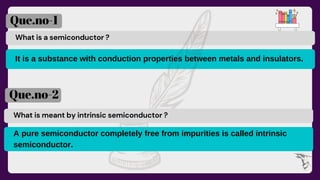
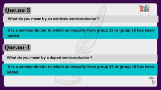
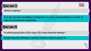
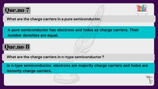
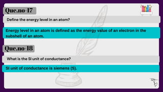
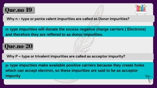
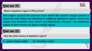
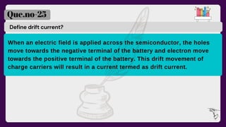
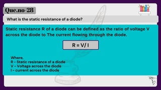
This document discusses key concepts related to PN junction diodes. It begins by defining a semiconductor as a material with conduction properties between metals and insulators. It then discusses intrinsic and extrinsic semiconductors, doping, and the charge carriers in pure, n-type, and p-type semiconductors. The document defines a junction diode as a structure formed by intimate contact of p-type and n-type semiconductors. It also discusses forward and reverse bias, knee voltage, reverse breakdown, Zener diodes, and their application as voltage regulators. Key diode parameters like barrier potential, reverse saturation current, static and dynamic resistance, and transition capacitance are also defined.
