The document provides specifications for an IRL3705N HEXFET Power MOSFET. Key details include:
- It has a maximum continuous drain current of 89A, drain-source breakdown voltage of 55V, and on-resistance as low as 0.01 ohms.
- It utilizes advanced processing for low resistance and fast switching capabilities. This provides high efficiency and reliability.
- It is available in a TO-220 package suitable for commercial/industrial applications up to 50 watts and features low thermal resistance.
Being an introvert seems like a fate, but in fact it‘s a challenge. Understand-
ing yourself will help you tackle the problems that all introverts are facing: health
risks, job-related problems and difficult relationships. Knowing about those intro-
vert specific issues will help you to lift your burden and to develop your true po-
tential. And as a result, you will live happier and healthier.
Original Mosfet IRF4905PBF IRF4905 IRF4905 4905 55V 74A TO-220 New Internatio...AUTHELECTRONIC
Original Mosfet IRF4905PBF IRF4905 IRF4905 4905 55V 74A TO-220 New International Rectifier
https://authelectronic.com/original-mosfet-irf4905pbf-irf4905-irf4905-4905-55v-74a-to-220-new-international-rectifier
Original P Channel Mosfet IRF9Z34 IRF9Z34N IRF9Z34NPBF 9Z34 60V 18A TO 220 NewAUTHELECTRONIC
Original P Channel Mosfet IRF9Z34 IRF9Z34N IRF9Z34NPBF 9Z34 60V 18A TO 220 New
https://authelectronic.com/original-p-channel-mosfet-irf9z34-irf9z34n-irf9z34npbf-9z34-60v-18a-to-220-new
Original N Channel Mosfet IRF3710PBF IRF3710 3710 37A 100V NewAUTHELECTRONIC
Original N Channel Mosfet IRF3710PBF IRF3710 3710 37A 100V New
https://authelectronic.com/original-n-channel-mosfet-irf3710pbf-irf3710-3710-37a-100v-new
Original P-CHANNEL MOSFET IRF5210PBF IRF5210 5210 100V 38A TO-220 New IRAUTHELECTRONIC
Original P-CHANNEL MOSFET IRF5210PBF IRF5210 5210 100V 38A TO-220 New IR
https://authelectronic.com/original-p-channel-mosfet-irf5210pbf-irf5210-5210-100v-38a-to-220-new-ir
Original N-Channel Power MOSFET IRF1010EPBF IRF1010 1010 60V 84A TO-220 New I...AUTHELECTRONIC
Original N-Channel Power MOSFET IRF1010EPBF IRF1010 1010 60V 84A TO-220 New International Rectifier
https://authelectronic.com/original-n-channel-power-mosfet-irf1010epbf-irf1010-1010-60v-84a-to-220-new-international-rectifier
Original Power MOSFET IRFP140PBF IRFP140 IRFP140N 100V 33A TO-247 New Intern...AUTHELECTRONIC
Original Power MOSFET IRFP140PBF IRFP140 IRFP140N 100V 33A TO-247 New International Rectifier
https://authelectronic.com/original-power-mosfet-irfp140pbf-irfp140-irfp140n-100v-33a-to-247-new-international-rectifier
Welcome to WIPAC Monthly the magazine brought to you by the LinkedIn Group Water Industry Process Automation & Control.
In this month's edition, along with this month's industry news to celebrate the 13 years since the group was created we have articles including
A case study of the used of Advanced Process Control at the Wastewater Treatment works at Lleida in Spain
A look back on an article on smart wastewater networks in order to see how the industry has measured up in the interim around the adoption of Digital Transformation in the Water Industry.
Overview of the fundamental roles in Hydropower generation and the components involved in wider Electrical Engineering.
This paper presents the design and construction of hydroelectric dams from the hydrologist’s survey of the valley before construction, all aspects and involved disciplines, fluid dynamics, structural engineering, generation and mains frequency regulation to the very transmission of power through the network in the United Kingdom.
Author: Robbie Edward Sayers
Collaborators and co editors: Charlie Sims and Connor Healey.
(C) 2024 Robbie E. Sayers
Industrial Training at Shahjalal Fertilizer Company Limited (SFCL)MdTanvirMahtab2
This presentation is about the working procedure of Shahjalal Fertilizer Company Limited (SFCL). A Govt. owned Company of Bangladesh Chemical Industries Corporation under Ministry of Industries.
Hierarchical Digital Twin of a Naval Power SystemKerry Sado
A hierarchical digital twin of a Naval DC power system has been developed and experimentally verified. Similar to other state-of-the-art digital twins, this technology creates a digital replica of the physical system executed in real-time or faster, which can modify hardware controls. However, its advantage stems from distributing computational efforts by utilizing a hierarchical structure composed of lower-level digital twin blocks and a higher-level system digital twin. Each digital twin block is associated with a physical subsystem of the hardware and communicates with a singular system digital twin, which creates a system-level response. By extracting information from each level of the hierarchy, power system controls of the hardware were reconfigured autonomously. This hierarchical digital twin development offers several advantages over other digital twins, particularly in the field of naval power systems. The hierarchical structure allows for greater computational efficiency and scalability while the ability to autonomously reconfigure hardware controls offers increased flexibility and responsiveness. The hierarchical decomposition and models utilized were well aligned with the physical twin, as indicated by the maximum deviations between the developed digital twin hierarchy and the hardware.
Sachpazis:Terzaghi Bearing Capacity Estimation in simple terms with Calculati...Dr.Costas Sachpazis
Terzaghi's soil bearing capacity theory, developed by Karl Terzaghi, is a fundamental principle in geotechnical engineering used to determine the bearing capacity of shallow foundations. This theory provides a method to calculate the ultimate bearing capacity of soil, which is the maximum load per unit area that the soil can support without undergoing shear failure. The Calculation HTML Code included.
Cosmetic shop management system project report.pdfKamal Acharya
Buying new cosmetic products is difficult. It can even be scary for those who have sensitive skin and are prone to skin trouble. The information needed to alleviate this problem is on the back of each product, but it's thought to interpret those ingredient lists unless you have a background in chemistry.
Instead of buying and hoping for the best, we can use data science to help us predict which products may be good fits for us. It includes various function programs to do the above mentioned tasks.
Data file handling has been effectively used in the program.
The automated cosmetic shop management system should deal with the automation of general workflow and administration process of the shop. The main processes of the system focus on customer's request where the system is able to search the most appropriate products and deliver it to the customers. It should help the employees to quickly identify the list of cosmetic product that have reached the minimum quantity and also keep a track of expired date for each cosmetic product. It should help the employees to find the rack number in which the product is placed.It is also Faster and more efficient way.
Original Mosfet L3705N L3705 3705 55V 75A TO-220 New
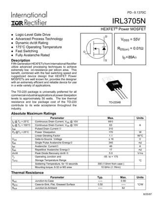
1. IRL3705N
HEXFET® Power MOSFET
PD - 9.1370C
S
D
G
VDSS = 55V
RDS(on) = 0.01Ω
ID=89A…
l Logic-Level Gate Drive
l Advanced Process Technology
l Dynamic dv/dt Rating
l 175°C Operating Temperature
l Fast Switching
l Fully Avalanche Rated
Fifth Generation HEXFETs from International Rectifier
utilize advanced processing techniques to achieve
extremely low on-resistance per silicon area. This
benefit, combined with the fast switching speed and
ruggedized device design that HEXFET Power
MOSFETs are well known for, provides the designer
with an extremely efficient and reliable device for use
in a wide variety of applications.
The TO-220 package is universally preferred for all
commercial-industrialapplicationsatpowerdissipation
levels to approximately 50 watts. The low thermal
resistance and low package cost of the TO-220
contribute to its wide acceptance throughout the
industry.
Description
TO-220AB
8/25/97
Parameter Max. Units
ID @ TC = 25°C Continuous Drain Current, VGS @ 10V 89…
ID @ TC = 100°C Continuous Drain Current, VGS @ 10V 63 A
IDM Pulsed Drain Current 310
PD @TC = 25°C Power Dissipation 170 W
Linear Derating Factor 1.1 W/°C
VGS Gate-to-Source Voltage ± 16 V
EAS Single Pulse Avalanche Energy‚ 340 mJ
IAR Avalanche Current 46 A
EAR Repetitive Avalanche Energy 17 mJ
dv/dt Peak Diode Recovery dv/dt ƒ 5.0 V/ns
TJ Operating Junction and -55 to + 175
TSTG Storage Temperature Range
Soldering Temperature, for 10 seconds 300 (1.6mm from case )
°C
Mounting torque, 6-32 or M3 srew 10 lbf•in (1.1N•m)
Absolute Maximum Ratings
Parameter Typ. Max. Units
RθJC Junction-to-Case ––– 0.90
RθCS Case-to-Sink, Flat, Greased Surface 0.50 ––– °C/W
RθJA Junction-to-Ambient ––– 62
Thermal Resistance
2. IRL3705N
Parameter Min. Typ. Max. Units Conditions
V(BR)DSS Drain-to-Source Breakdown Voltage 55 ––– ––– V VGS = 0V, ID = 250µA
∆V(BR)DSS/∆TJ Breakdown Voltage Temp. Coefficient ––– 0.056 ––– V/°C Reference to 25°C, ID = 1mA
––– ––– 0.010 VGS = 10V, ID = 46A „
––– ––– 0.012 Ω VGS = 5.0V, ID = 46A „
––– ––– 0.018 VGS = 4.0V, ID = 39A „
VGS(th) Gate Threshold Voltage 1.0 ––– 2.0 V VDS = VGS, ID = 250µA
gfs Forward Transconductance 50 ––– ––– S VDS = 25V, ID = 46A
––– ––– 25
µA
VDS = 55V, VGS = 0V
––– ––– 250 VDS = 44V, VGS = 0V, TJ = 150°C
Gate-to-Source Forward Leakage ––– ––– 100
nA
VGS = 16V
Gate-to-Source Reverse Leakage ––– ––– -100 VGS = -16V
Qg Total Gate Charge ––– ––– 98 ID = 46A
Qgs Gate-to-Source Charge ––– ––– 19 nC VDS = 44V
Qgd Gate-to-Drain ("Miller") Charge ––– ––– 49 VGS = 5.0V, See Fig. 6 and 13 „
td(on) Turn-On Delay Time ––– 12 ––– VDD = 28V
tr Rise Time ––– 140 –––
ns
ID = 46A
td(off) Turn-Off Delay Time ––– 37 ––– RG = 1.8Ω, VGS = 5.0V
tf Fall Time ––– 78 ––– RD = 0.59Ω, See Fig. 10 „
Between lead,
6mm (0.25in.)
from package
and center of die contact
Ciss Input Capacitance ––– 3600 ––– VGS = 0V
Coss Output Capacitance ––– 870 ––– pF VDS = 25V
Crss Reverse Transfer Capacitance ––– 320 ––– ƒ = 1.0MHz, See Fig. 5
Electrical Characteristics @ TJ = 25°C (unless otherwise specified)
nH
IGSS
S
D
G
LS Internal Source Inductance ––– 7.5 –––
RDS(on) Static Drain-to-Source On-Resistance
LD Internal Drain Inductance ––– 4.5 –––
IDSS Drain-to-Source Leakage Current
Parameter Min. Typ. Max. Units Conditions
IS Continuous Source Current MOSFET symbol
(Body Diode)
––– –––
showing the
ISM Pulsed Source Current integral reverse
(Body Diode)
––– –––
p-n junction diode.
VSD Diode Forward Voltage ––– ––– 1.3 V TJ = 25°C, IS = 46A, VGS = 0V „
trr Reverse Recovery Time ––– 94 140 ns TJ = 25°C, IF = 46A
Qrr Reverse RecoveryCharge ––– 290 440 nC di/dt = 100A/µs „
ton Forward Turn-On Time Intrinsic turn-on time is negligible (turn-on is dominated by LS+LD)
Source-Drain Ratings and Characteristics
S
D
G
89…
310
A
Repetitive rating; pulse width limited by
max. junction temperature. ( See fig. 11 )
ƒ ISD ≤ 46A, di/dt ≤ 250A/µs, VDD ≤ V(BR)DSS,
TJ ≤ 175°C
Notes:
‚ VDD = 25V, starting TJ = 25°C, L = 320µH
RG = 25Ω, IAS = 46A. (See Figure 12)
„ Pulse width ≤ 300µs; duty cycle ≤ 2%.
… Calculated continuous current based on maximum allowable
junction temperature; for recommended current-handling of the
package refer to Design Tip # 93-4
3. IRL3705N
Fig 1. Typical Output Characteristics
Fig 3. Typical Transfer Characteristics
Fig 2. Typical Output Characteristics
Fig 4. Normalized On-Resistance
Vs. Temperature
1
10
100
1000
0.1 1 10 100
I,Drain-to-SourceCurrent(A)D
V , Drain-to-Source Voltage (V)DS
A
20µs PULSE W IDTH
T = 25°CJ
VGS
TOP 15V
12V
10V
8.0V
6.0V
4.0V
3.0V
BOTTOM 2.5V
2.5V
1
10
100
1000
0.1 1 10 100I,Drain-to-SourceCurrent(A)D
V , Drain-to-Source Voltage (V)DS
A
20µs PULSE W IDTH
T = 175°C
VGS
TOP 15V
12V
10V
8.0V
6.0V
4.0V
3.0V
BOTTOM 2.5V
2.5V
J
1
1 0
1 0 0
1 0 0 0
2.0 3.0 4.0 5.0 6.0 7.0 8.0
T = 25°CJ
G SV , Gate-to-Source Voltage (V)
DI,Drain-to-SourceCurrent(A)
T = 175°CJ
A
V = 25V
20µs PULSE W IDTH
DS
0.0
0.5
1.0
1.5
2.0
2.5
3.0
-60 -40 -20 0 2 0 4 0 6 0 8 0 1 0 0 1 2 0 1 4 0 1 6 0 1 8 0
JT , Junction Temperature (°C)
R,Drain-to-SourceOnResistanceDS(on)
(Normalized)
V = 10VGS
A
I = 77AD
4. IRL3705N
Fig 8. Maximum Safe Operating Area
Fig 6. Typical Gate Charge Vs.
Gate-to-Source Voltage
Fig 5. Typical Capacitance Vs.
Drain-to-Source Voltage
Fig 7. Typical Source-Drain Diode
Forward Voltage
0
1000
2000
3000
4000
5000
6000
1 10 100
C,Capacitance(pF)
DSV , Drain-to-Source Voltage (V)
A
V = 0V , f = 1MHz
C = C + C , C SHORTED
C = C
C = C + C
GS
iss gs gd ds
rss g d
oss ds gdC is s
C os s
C rs s
0
3
6
9
12
15
0 20 40 60 80 100 120 140
Q , Total Gate Charge (nC)G
V,Gate-to-SourceVoltage(V)GS
A
FOR TES T CIRCUIT
SEE FIGURE 13
I = 46A
V = 44V
V = 28V
D
DS
DS
1 0
1 0 0
1 0 0 0
0.4 0.8 1.2 1.6 2.0 2.4 2.8
T = 25°CJ
V = 0VGS
V , Source-to-Drain Voltage (V)
I,ReverseDrainCurrent(A)
SD
SD
A
T = 175°CJ
1
10
100
1000
1 10 100
V , Drain-to-Source Voltage (V)DS
I,DrainCurrent(A)
OPE RATION IN THIS A RE A LIMITE D
BY R
D
D S(on)
10µs
100µs
1ms
10ms
A
T = 25°C
T = 175°C
S ingle Pulse
C
J
5. IRL3705N
Fig 9. Maximum Drain Current Vs.
Case Temperature
Fig 10a. Switching Time Test Circuit
VDS
90%
10%
VGS
td(on) tr td(off) tf
Fig 10b. Switching Time Waveforms
VDS
Pulse Width ≤ 1 µs
Duty Factor ≤ 0.1 %
RD
VGS
RG
D.U.T.
5.0V
+
-VDD
Fig 11. Maximum Effective Transient Thermal Impedance, Junction-to-Case
25 50 75 100 125 150 175
0
20
40
60
80
100
T , Case Temperature ( C)
I,DrainCurrent(A)
°C
D
LIMITED BY PACKAGE
0.01
0.1
1
0.00001 0.0001 0.001 0.01 0.1 1
Notes:
1. Duty factor D = t / t
2. Peak T = P x Z + T
1 2
J DM thJC C
P
t
t
DM
1
2
t , Rectangular Pulse Duration (sec)
ThermalResponse(Z)
1
thJC
0.01
0.02
0.05
0.10
0.20
D = 0.50
SINGLE PULSE
(THERMAL RESPONSE)
6. IRL3705N
QG
QGS QGD
VG
Charge
5.0 V
Fig 13b. Gate Charge Test CircuitFig 13a. Basic Gate Charge Waveform
Fig 12c. Maximum Avalanche Energy
Vs. Drain Current
D.U.T.
VDS
IDIG
3mA
VGS
.3µF
50KΩ
.2µF12V
Current Regulator
Same Type as D.U.T.
Current Sampling Resistors
+
-
0
200
400
600
800
25 50 75 100 125 150 175
J
E,SinglePulseAvalancheEnergy(mJ)AS A
Starting T , Junction Temperature (°C)
V = 25V
I
TOP 19A
33A
BOTTOM 46A
D D
D
Fig 12b. Unclamped Inductive Waveforms
Fig 12a. Unclamped Inductive Test Circuit
tp
V(BR)DSS
IAS
R G
IA S
0.01Ωtp
D .U .T
LVD S
+
-
VD D
D R IV ER
A
15 V
10V
7. IRL3705N
P.W.
Period
di/dt
Diode Recovery
dv/dt
Ripple ≤ 5%
Body Diode Forward Drop
Re-Applied
Voltage
Reverse
Recovery
Current
Body Diode Forward
Current
VGS=10V
VDD
ISD
Driver Gate Drive
D.U.T. ISD Waveform
D.U.T. VDS Waveform
Inductor Curent
D =
P.W.
Period
+
-
+
+
+-
-
-
Fig 14. For N-Channel HEXFETS
* VGS = 5V for Logic Level Devices
Peak Diode Recovery dv/dt Test Circuit
ƒ
„
‚
RG
VDD
• dv/dt controlled by RG
• Driver same type as D.U.T.
• ISD controlled by Duty Factor "D"
• D.U.T. - Device Under Test
D.U.T
Circuit Layout Considerations
• Low Stray Inductance
• Ground Plane
• Low Leakage Inductance
Current Transformer
*
8. IRL3705N
PART NUMBERINTERNATIONAL
RECTIFIER
LOGO
EXAMPLE : THIS IS AN IRF1010
W ITH ASSEMBLY
LOT CODE 9B1M
ASSEMBLY
LOT CODE
DATE CODE
(YYW W )
YY = YEAR
W W = W EEK
9246
IRF1010
9B 1M
A
Part Marking Information
TO-220AB
Package Outline
TO-220AB Outline
Dimensions are shown in millimeters (inches)
PART NUMBERINTERNATIONAL
RECTIFIER
LOGO
EXAMPLE : THIS IS AN IRF1010
W ITH ASSEMBLY
LOT CODE 9B1M
ASSEMBLY
LOT CODE
DATE CODE
(YYW W )
YY = YEAR
W W = W EEK
9246
IRF1010
9B 1M
A
L E AD A S S IG N M E N T S
1 - G A T E
2 - D R AIN
3 - S O U R C E
4 - D R AIN
- B -
1 .3 2 (.0 52 )
1 .2 2 (.0 48 )
3X
0.5 5 (.02 2)
0.4 6 (.01 8)
2 .9 2 (.11 5 )
2 .6 4 (.10 4 )
4 .69 ( .1 85 )
4 .20 ( .1 65 )
3X
0 .93 ( .0 37 )
0 .69 ( .0 27 )
4.0 6 (.16 0)
3.5 5 (.14 0)
1.15 ( .0 4 5)
M IN
6.4 7 (.25 5)
6.1 0 (.24 0)
3.78 (.14 9)
3.54 (.13 9)
- A -
1 0.5 4 (.41 5)
1 0.2 9 (.40 5)2 .87 ( .1 13 )
2 .62 ( .1 03 )
1 5.24 ( .6 0 0)
1 4.84 ( .5 8 4)
1 4.09 (.5 5 5)
1 3.47 (.5 3 0)
3 X
1 .4 0 (.05 5 )
1 .1 5 (.04 5 )
2 .54 ( .1 00 )
2X
0 .3 6 (.01 4) M B A M
4
1 2 3
N O T E S :
1 D IM E N S IO N IN G & T O L ER AN C IN G P ER A N S I Y 14 .5 M , 1 98 2. 3 O U T L IN E C O N F O R M S T O JE D E C O U T LIN E T O -2 20 A B.
2 C O N T R O L LIN G D IM E N S IO N : IN C H 4 H EA T S IN K & L E AD M EA S U R E M E N T S D O N O T IN C L U D E BU R R S .
WORLD HEADQUARTERS: 233 Kansas St., El Segundo, California 90245, Tel: (310) 322 3331
EUROPEAN HEADQUARTERS: Hurst Green, Oxted, Surrey RH8 9BB, UK Tel: ++ 44 1883 732020
IR CANADA: 7321 Victoria Park Ave., Suite 201, Markham, Ontario L3R 2Z8, Tel: (905) 475 1897
IR GERMANY: Saalburgstrasse 157, 61350 Bad Homburg Tel: ++ 49 6172 96590
IR ITALY: Via Liguria 49, 10071 Borgaro, Torino Tel: ++ 39 11 451 0111
IR FAR EAST: K&H Bldg., 2F, 30-4 Nishi-Ikebukuro 3-Chome, Toshima-Ku, Tokyo Japan 171 Tel: 81 3 3983 0086
IR SOUTHEAST ASIA: 315 Outram Road, #10-02 Tan Boon Liat Building, Singapore 0316 Tel: 65 221 8371
http://www.irf.com/ Data and specifications subject to change without notice. 8/97
9. Note: For the most current drawings please refer to the IR website at:
http://www.irf.com/package/