Download to read offline
![Lekashri S. Int. Journal of Engineering Research and Applications www.ijera.com
ISSN: 2248-9622, Vol. 6, Issue 4, (Part - 7) April 2016, pp.45-48
www.ijera.com 46|P a g e
Figure 2: An Input Assignment
III. CONFIGURATION GENERATION
ALGORITTHM
The process of assigning activating inputs
and test vectors in the configurations for the nets
starts by extracting the interconnect features of a
specific circuit mapped to an FGPA (in this case, this
is given by the Vertex 4) from the Native Generic
Database (NGD) of the design. The NGD is
converted to a text file and then the nets are sorted
based on the number of connected LUTs. A greedy
criterion for selecting the activating inputs and test
vectors is used as follows: The first activating input is
assigned to a net that is connected to the largest
number of LUTs, followed by assigning the second
and third activating inputs to the other nets in a
descending order. However, during each activating
input assignment, it must be ensured that no two (or
more) nets connected to a LUT are driven by the
same activating input. In the case of two nets
connected to the same LUT having the same
activating input, one of the activating inputs is
assigned to the next available activating input to
resolve the conflict. The pseudo code for the above
process as given in the induction method of Tahoori
[3] is utilized for propagating the sensitized faults to
the primary output, thus accomplishing observability
in detection.
At completion of the algorithm, the
activating inputs to the LUTs are found and hence,
the corresponding test configurations can be
determined.
IV. PROPOSED METHOD
Optimization of test patterns for testing
SRAM using genetic algorithm is been proposed. The
novelty of this comprehensive method is that it
connects an activating input to multiple nets, thus
generating a compact set of activating test vectors and
requiring a reduced numbers of configurations. The
faults covered in this technique include all possible
stuck-at, open, and pair wise bridging faults.
However, to allow a fair comparison with existing
works logic simulation is therefore employed also in
this paper; therefore, all possible stuck-at, open, and
pair wise bridging faults are considered and detected
by the proposed approach. So, for detecting the faults
at the primary outputs, the induction fault detection
method is adopted. The proposed method optimizes
the test pattern in execution .This is lower than a
previous comprehensive method. The proposed
method has a genetic algorithm execution. Therefore,
the proposed method differs from previous
approaches with respect to test pattern. The test
patterns are generated by using Linear feedback shift
register (LFSR).
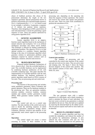
An LFSR is a shift register with feedbacks
from the last stage and other stages. The outputs of its
flip-flops form the test pattern. Each state of the
LFSR corresponds to one test pattern. The number of
unique test patterns the LFSR can generate depends
on the number and location of the feedbacks as well
as its initial value, which is known as the seed. An
example of an LFSR is shown in Figure 3
Figure 3: LFSR Example
It is initialized with the seed 0001. In the
subsequent clock cycles, a series of test patterns are
produced at the outputs of the flip-flops. This LFSR,
which has n=4 flip-flops, produces a total of 15 (2n -
1) distinct patterns (except 0000) as shown in
Figure.3. The feedback positions are usually
described by a characteristic polynomial. In our
example, feedbacks are made from the first (x) and
the fourth (x4) positions, hence the characteristic
polynomial of the LFSR is p(x) = 1 + x + x4. The
0 0 0 1
1 0 0 0
1 1 0 0
1 1 1 0
1 1 1 1
0 1 1 1
1 0 1 1
0 1 0 0
1 0 1 1
1 1 0 0
0 1 1 0
0 0 1 1
1 0 0 1
0 1 0 0
0 0 1 0
0 0 0 1](https://image.slidesharecdn.com/i0604074548-160810113344/85/Optimization-of-Test-Pattern-Using-Genetic-Algorithm-for-Testing-SRAM-2-320.jpg)
![Lekashri S. Int. Journal of Engineering Research and Applications www.ijera.com
ISSN: 2248-9622, Vol. 6, Issue 4, (Part - 7) April 2016, pp.45-48
www.ijera.com 48|P a g e
used for testing and fault analysis of the circuit. The
simulated output of without fault and with fault are
shown below in fig 6 & fig 7 respectively. Thus the
observed results from the proposed architecture
achieves minimum power in the range of 220-230
mW and the reduced time constraint is about 1.5-2 ns.
Figure 6: Without Fault
Figure 7: With Fault
VIII. CONCLUSION
Thus genetic algorithmic method for
optimizing test pattern for testing of a SRAM that is
been proposed relies on generating minimized test
patterns. This algorithmic-based method detects all
stuck-at, open, and pair wise bridging faults,
optimizes test patterns with minimum time constraint
and less power consumption.
REFERENCES
[1] M. J. O'Dare and T. Arslan,”Generating Test
Patterns For Vlsi Circuits Using A Genetic
Algorithm” ,U.K.
[2] Lalit A. Patel, Sarman K. Hadia,“Transistor
Level Fault Finding in VLSI Circuits using
Genetic Algorithm “
[3] M.B. Tahoori, “Application-Dependent
Testing of FPGAs,” IEEE Trans. Very Large
Scale Integration Systems, vol. 14, no. 9, pp.
1024- 1033, Sept. 2006.
[4] M.B. Tahoori, “Application-Dependent
Testing of FPGA Interconnects,” Proc. 18th
IEEE Int’l Symp. Defect and Fault
Tolerance in VLSI Systems, pp. 409-416,
Nov. 2003.
[5] M.B. Tahoori, “Application-Dependent
Diagnosis of FPGAs,” Proc. IEEE Int’l Test
Conf., pp. 645-654, Oct. 2004.
[6] A. Doumar and H. Ito, “Testing the Logic
Cells and Interconnect Resources for
FPGAs,” Proc. Eighth Asian Test Symp., pp.
369-374, Nov. 1999.
[7] Y. Yu, J. Xu, W.K. Huang, and F.
Lombardi, “A Diagnosis Method for
Interconnects in SRAM Based FPGAs,”
Proc. Seventh Asian Test Symp., pp. 278-
282, Dec. 1998.
[8] W.K. Huang, X.T. Chen, and F. Lombardi,
“On the Diagnosis of Programmable
Interconnect System: Theory and
Application,” Proc. 14th VLSl Test Symp.,
pp. 204-209, Apr. 1996.
[9] F. Lombardi, D. Ashen, X. Chen, and W.K.
Huang, “Diagnosing Programmable
Interconnect System for FPGAs,” Proc.
Fourth ACM Int’l Symp. Field-
Programmable Gate Arrays, pp. 100-106,
1996.
[10] Feng Liang, Luwen Zhang, Shaochong Lei,
Guohe Zhang, Kaile Gao an](https://image.slidesharecdn.com/i0604074548-160810113344/85/Optimization-of-Test-Pattern-Using-Genetic-Algorithm-for-Testing-SRAM-4-320.jpg)

This document proposes optimizing test patterns for testing SRAM using genetic algorithms. The genetic algorithm approach generates a compact set of test vectors requiring fewer configurations while detecting all stuck-at, open, and bridging faults. It reduces redundancy and optimizes the test patterns, resulting in reduced testing time and power consumption compared to previous methods. The optimized test patterns are generated using a linear feedback shift register and genetic operations including selection, crossover and mutation. Results show the proposed method achieves fault detection with a minimum time constraint of 1.5-2 ns and low power consumption of 220-230 mW.


![208224019-20_testing_ppt[1][1][1]_1[1][1].pptx](https://cdn.slidesharecdn.com/ss_thumbnails/208224019-20testingppt111111-250415093818-44899f27-thumbnail.jpg?width=640&height=640&fit=bounds)


