Download to read offline
![Advanced Nanoscience and Technology: An International Journal (ANTJ), Vol. 3, No.1/2, June 2017
DOI: 10.5121/antj.2017.3201 1
ON APPROACH TO INCREASE DENSITY OF FIELD-
EFFECT TRANSISTORS IN AN INVERTER CIRCUIT
E.L. Pankratov and E.A. Bulaeva
Nizhny Novgorod State University, 23 Gagarin avenue, Nizhny Novgorod, 603950,
Russia
ABSTRACT
In this paper we consider an approach to decrease dimensions of field-effect transistors framework
invertors with increasing of their density. Framework the approach it is necessary to manufacture a
heterostructure, which consist of two layers. One of them includes into itself several sections. After
manufacturing of the heterostructure these sections should be doped by diffusion or by ion implantation
with future optimized annealing of dopant and/or radiation defects. To prognosis the technological
process we consider an analytical approach, which gives a possibility to take into account variation of
physical parameters in space and time. At the same time the approach gives a possibility to take into
account nonlinearity of mass and heat transport and to analyze the above transport without crosslink-
ing solutions on interfaces between materials of heterostructure.
KEYWORDS
Field-effect heterotransystors, inverters dynamic and resistive loads, decreasing of dimensions, optimiza-
tion of manufacturing.
1. INTRODUCTION
Intensive development of solid state electronics gives a possibility to increase density of elements
of integrated circuits, reliability and performances of their elements (diodes, field-effect and bipo-
lar transistors, et al) and their discrete analogs. Increasing of density of elements of integrated
circuits leads to necessity to decrease their dimensions. One way to decrease dimensions of ele-
ments of integrated circuits is their manufacturing framework thin film heterostructures [1-4]. An
alternative approach to decrease their dimensions is using laser and microwave types of anneal-
ing [5-7]. Both types of annealing gives a possibility to generate inhomogenous distribution of
temperature. In this situation one can obtain inhomogenous distribution of diffusion coefficients
of dopants and radiation defects and other parameters. The inhomogeneity gives a possibility to
decrease dimensions of elements of integrated circuits. Properties of electronic materials could be
also changed by radiation processing [8,9].
In the present paper we consider circuits of invertors with dynamic and resistive loads [10] (see
Fig. 1). Based on recently formulated recommendations to decrease dimensions of single transis-
tors (both bipolar and field-effect) [11-16] we formulate recommendations to increase density of
field-effect transistors framework the considered circuits. We assume, that the considered circuits
were manufactured framework the considered in Fig.1 heterostructure. The heterostructure con-
sist of a substrate and an epitaxial layer. The epitaxial layer includes into itself several sections,
manufactured by using other materials. These sections were doped by diffusion or by ion implan-
tation to generate required types of conductivity (n or p) in the required materials. Framework this
paper we analyzed redistribution of dopants during annealing of these dopants and/or radiation
defects to formulate conditions, which correspond to decreasing of the considered circuits.](https://image.slidesharecdn.com/3217antj01-170712050218/75/ON-APPROACH-TO-INCREASE-DENSITY-OF-FIELD-EFFECT-TRANSISTORS-IN-AN-INVERTER-CIRCUIT-1-2048.jpg)
![Advanced Nanoscience and Technology: An International Journal (ANTJ), Vol. 3, No.1/2, June 2017
2
Fig. 1a. Structure of Inverter With Dynamic Load. Fig. 1b. Structure of inverter with resistive load.
View from top View From Top
2. METHOD OF SOLUTION
To solve our aim we shall analyze spatio-temporal distribution of concentration of dopant. The
distribution has been determined by solving the following boundary problem
z
tzyxC
D
zy
tzyxC
D
yx
tzyxC
D
xt
tzyxC
CCC
,,,,,,,,,,,,
. (1)
Boundary and initial conditions for the equations are
0
,,,
0
x
x
tzyxC
,
0
,,,
xLx
x
tzyxC
,
0
,,,
0
y
y
tzyxC
,
0
,,,
yLx
y
tzyxC
,
0
,,,
0
z
z
tzyxC
,
0
,,,
zLx
z
tzyxC
, C (x,y,z,0)=f (x,y,z). (2)
Function C(x,y,z,t) describes the spatio-temporal distribution of concentration of dopant; T is the
temperature of annealing; DС is the dopant diffusion coefficient. Value of dopant diffusion coeffi-
cient will be different in different materials and will be changed with changing of temperature of
annealing (with account Arrhenius law). The value also depends on concentrations of dopant and
radiation defects. All above dependences could be accounted by the following relation [9, 17,18]
2*
2
2*1
,,,,,,
1
,,,
,,,
1,,,
V
tzyxV
V
tzyxV
TzyxP
tzyxC
TzyxDD LC
.(3)](https://image.slidesharecdn.com/3217antj01-170712050218/75/ON-APPROACH-TO-INCREASE-DENSITY-OF-FIELD-EFFECT-TRANSISTORS-IN-AN-INVERTER-CIRCUIT-2-2048.jpg)
![Advanced Nanoscience and Technology: An International Journal (ANTJ), Vol. 3, No.1/2, June 2017
3
The function DL(x,y,z,T) gives a possibility to take into account the spatial and temperature de-
pendences of dopant diffusion coefficient (due to presents several layers in heterostructure and
Arrhenius law). The function P (x,y,z,T) describes the limit of solubility of dopant. The parameter
[1,3] describes quantity of charged defects, which were interacted (in average) with atoms of
dopant [17]. The function V (x,y,z,t) describes the spatio-temporal distribution of concentration of
radiation vacancies. The parameter V*
describes the equilibrium distribution of concentration of
vacancies. It should be noted, that using diffusion type of doping did not generation radiation de-
fects. In this situation 1=2=0. We determine spatio-temporal distributions of concentrations of
radiation defects by solving the following system of equations [9,18]
Tzyxk
y
tzyxI
TzyxD
yx
tzyxI
TzyxD
xt
tzyxI
IIII ,,,
,,,
,,,
,,,
,,,
,,,
,
tzyxVtzyxITzyxk
z
tzyxI
TzyxD
z
tzyxI VII ,,,,,,,,,
,,,
,,,,,, ,
2
(4)
Tzyxk
y
tzyxV
TzyxD
yx
tzyxV
TzyxD
xt
tzyxV
VVVV ,,,
,,,
,,,
,,,
,,,
,,,
,
tzyxVtzyxITzyxk
z
tzyxV
TzyxD
z
tzyxV VIV ,,,,,,,,,
,,,
,,,,,, ,
2
.
Boundary and initial conditions for these equations are
0
,,,
0
x
x
tzyx
,
0
,,,
xLx
x
tzyx
,
0
,,,
0
y
y
tzyx
,
0
,,,
yLy
y
tzyx
,
0
,,,
0
z
z
tzyx
,
0
,,,
zLz
z
tzyx
, (x,y,z,0)=f (x,y,z). (5)
Here =I,V. The function I(x,y,z,t) describes variation of distribution of concentration of radiation
interstitials in space and time. The function D(x,y,z,T) describes dependences of the diffusion
coefficients of point radiation defects on spatial coordinates and temperature. Terms V2
(x,y,z,t)
and I2
(x,y,z,t) correspond to generation divacancies and diinterstitials; kI,V(x,y,z,T) is the parameter
of recombination of point radiation defects; kI,I(x,y,z,T) and kV,V(x,y,z,T) are the parameters of
generation of simplest complexes of point radiation defects.
We determine concentrations of divacancies V (x,y,z,t) and dinterstitials I (x,y,z,t) as functions
of space and time by solving the following system of equations [17,18]
y
tzyx
TzyxD
yx
tzyx
TzyxD
xt
tzyx I
I
I
I
I
,,,
,,,
,,,
,,,
,,,
tzyxITzyxktzyxITzyxk
z
tzyx
TzyxD
z
III
I
I ,,,,,,,,,,,,
,,,
,,, 2
,
(6)
y
tzyx
TzyxD
yx
tzyx
TzyxD
xt
tzyx V
V
V
V
V
,,,
,,,
,,,
,,,
,,,
tzyxVTzyxktzyxVTzyxk
z
tzyx
TzyxD
z
VVV
V
V ,,,,,,,,,,,,
,,,
,,, 2
,
.](https://image.slidesharecdn.com/3217antj01-170712050218/75/ON-APPROACH-TO-INCREASE-DENSITY-OF-FIELD-EFFECT-TRANSISTORS-IN-AN-INVERTER-CIRCUIT-3-2048.jpg)
![Advanced Nanoscience and Technology: An International Journal (ANTJ), Vol. 3, No.1/2, June 2017
4
Boundary and initial conditions for these equations are
0
,,,
0
x
x
tzyx
,
0
,,,
xLx
x
tzyx
,
0
,,,
0
y
y
tzyx
,
0
,,,
yLy
y
tzyx
,
0
,,,
0
z
z
tzyx
,
0
,,,
zLz
z
tzyx
, I (x,y,z,0)=fI (x,y,z), V (x,y,z,0)=fV (x,y,z). (7)
Here D(x,y,z,T) are the diffusion coefficients of the above complexes of radiation defects;
kI(x,y,z,T) and kV (x,y,z,T) are the parameters of decay of these complexes.
We determine spatio-temporal distributions of concentrations of dopant and radiation defects by
using method of averaging of function corrections [19] with decreased quantity of iteration steps
[20]. Framework the approach we used solutions of Eqs. (1), (4) and (6) in linear form and with
averaged values of diffusion coefficients D0L, D0I, D0V, D0I, D0V as initial-order approximations
of the required concentrations. The solutions could be written as
1
0
1
2
,,,
n
nCnnnnC
zyxzyx
C
tezcycxcF
LLLLLL
F
tzyxC ,
1
0
1
2
,,,
n
nInnnnI
zyxzyx
I
tezcycxcF
LLLLLL
F
tzyxI ,
1
0
1
2
,,,
n
nVnnnnC
zyxzyx
C
tezcycxcF
LLLLLL
F
tzyxV ,
1
0
1
2
,,,
n
nnnnn
zyxzyx
I tezcycxcF
LLLLLL
F
tzyx II
I
,
1
0
1
2
,,,
n
nnnnn
zyxzyx
V tezcycxcF
LLLLLL
F
tzyx VV
V
,
where
2220
22 111
exp
zyx
n
LLL
tDnte ,
x y zL L L
nnnn udvdwdwvufvcvcucF
0 0 0
,, , cn() =
cos(n/L).
We consider the above solutions as initial-order approximations of concentrations of dopant and
radiation defects.
Approximations of concentrations of dopant and radiation defects with the second and higher or-
ders could be determine framework standard iterative procedure [19,20]. The procedure based on
replacement of the functions C(x,y,z,t), I(x,y,z,t), V(x,y,z,t), I(x,y,z, t), V(x,y,z,t) in the right
sides of the Eqs. (1), (4) and (6) on the following sums n+ n-1(x,y,z,t). Framework the standard
iterative procedure we obtain equations for the second-order approximations of concentrations of
dopant and radiation defects
TzyxP
tzyxC
V
tzyxV
V
tzyxV
xt
tzyxC C
,,,
,,,
1
,,,,,,
1
,,, 12
2
2
21
2
](https://image.slidesharecdn.com/3217antj01-170712050218/75/ON-APPROACH-TO-INCREASE-DENSITY-OF-FIELD-EFFECT-TRANSISTORS-IN-AN-INVERTER-CIRCUIT-4-2048.jpg)

![Advanced Nanoscience and Technology: An International Journal (ANTJ), Vol. 3, No.1/2, June 2017
6
t
LC
C
L TzyxD
z
zyxfd
y
zyxC
TzyxP
zyxC
TzyxD
0
112
,,,,,
,,,
,,,
,,,
1,,,
d
z
zyxC
TzyxP
zyxC
V
zyxV
V
zyxV C ,,,
,,,
,,,
1
,,,,,,
1 112
2
2
21 (8a)
t
I
t
I d
y
zyxI
TzyxD
y
d
x
zyxI
TzyxD
x
tzyxI
0
1
0
1
2
,,,
,,,
,,,
,,,,,,
t
III
t
I dzyxITzyxkd
z
zyxI
TzyxD
z 0
2
12,
0
1
,,,,,,
,,,
,,,
t
VIVII dzyxVzyxITzyxkzyxf
0
1212, ,,,,,,,,,,, (9a)
t
V
t
V d
y
zyxV
TzyxD
y
d
x
zyxV
TzyxD
x
tzyxV
0
1
0
1
2
,,,
,,,
,,,
,,,,,,
t
IVV
t
V dzyxVTzyxkd
z
zyxV
TzyxD
z
d
y
zyxV
0
2
12,
0
11
,,,,,,
,,,
,,,
,,,
t
VIVIV dzyxVzyxITzyxkzyxf
0
1212, ,,,,,,,,,,,
t
I
t
I
I d
y
zyx
TzyxD
y
d
x
zyx
TzyxD
x
tzyx II
0
1
0
1
2
,,,
,,,
,,,
,,,,,,
t
II
t
I
dzyxITzyxkd
z
zyx
TzyxD
z I
0
2
,
0
1
,,,,,,
,,,
,,,
t
I dzyxITzyxkzyxf I
0
,,,,,,,, (10a)
t
V
t
V
V d
y
zyx
TzyxD
y
d
x
zyx
TzyxD
x
tzyx VV
0
1
0
1
2
,,,
,,,
,,,
,,,,,,
t
VV
t
V
dzyxVTzyxkd
z
zyx
TzyxD
z V
0
2
,
0
1
,,,,,,
,,,
,,,
t
V dzyxVTzyxkzyxf V
0
,,,,,,,,
Average values of the considered approximations have been determined by the following
relations [19,20]
0 0 0 0
122 ,,,,,,
1 x y zL L L
zyx
tdxdydzdtzyxtzyx
LLL
. (11)
Substitution of approximations (8a)-(10a) into the previous relation gives the possibility
to obtain relations for the average values 2 in the following final form](https://image.slidesharecdn.com/3217antj01-170712050218/75/ON-APPROACH-TO-INCREASE-DENSITY-OF-FIELD-EFFECT-TRANSISTORS-IN-AN-INVERTER-CIRCUIT-6-2048.jpg)

![Advanced Nanoscience and Technology: An International Journal (ANTJ), Vol. 3, No.1/2, June 2017
10
It should be noted, that framework the considered approach of manufacturing of transistor anneal-
ing should be optimized. Reason of the optimization is following. The main reason for this opti-
mization is following. If the annealing time is small, the dopant does not achieves any interfaces
between the materials of heterostructure. In this situation one can not find any modifications of
the distribution of concentration of dopant. If the annealing time is large, the distribution of con-
centration of dopant is too homogenous. We optimize the annealing time based on a recently in-
troduced approach [11-16]. By applying the criterion we approximate real distribution of concen-
tration of dopant by a step-wise function (see Figs. 4 and 5). Next we determine optimal values of
annealing time by minimization of the following mean-squared error
x y zL L L
zyx
xdydzdzyxtzyxC
LLL
U
0 0 0
,,,,,
1
, (15)
where (x,y,z) is the step-wise approximation of spatial distribution of concentration of dopant C
(x,y,z,t). We minimize the mean-squared error as the function of time. After the minimization we
obtain optimal value of annealing time . Dependences of optimal values of annealing time on
parameters are presented in Figs. 6 and 7 for diffusion and ion types of doping, respectively. It
should be noted, that it is necessary to anneal radiation defects after ion implantation. One could
find spreading of concentration of the distribution of concentration of dopant during this anneal-
ing. In the ideal case distribution of dopant achieves appropriate interfaces between materials of
heterostructure during annealing of radiation defects. If dopant does not achieve to the nearest
interface during annealing of radiation defects, it is practical to additionally anneal the dopant. In
this situation the optimal value of the additional annealing time of implanted dopant is smaller,
than the annealing time of infused dopant.
0.0 0.1 0.2 0.3 0.4 0.5
a/L, , ,
0.0
0.1
0.2
0.3
0.4
0.5
D0L
-2
3
2
4
1
Fig.6. Dependences of dimensionless optimal annealing time of infused dopant.
Curve 1 describes dimensionless optimal annealing time as the function of the relation a/L for =
=0 and for equal to each other values of dopant diffusion coefficient in all parts of heterostruc-
ture. Curve 2 describes dimensionless optimal annealing time as the function of the parameter
for a/L=1/2 and ==0 and for equal to each other values of dopant diffusion coefficient in all
parts of heterostructure. Curve 3 describes dimensionless optimal annealing time as the function
of the parameter for a/L=1/2 and ==0 and for equal to each other values of dopant diffusion
coefficient in all parts of heterostructure. Curve 4 describes dimensionless optimal annealing time
as the function of the parameter for a/L=1/2 and = =0 and for equal to each other values of
dopant diffusion coefficient in all parts of heterostructure](https://image.slidesharecdn.com/3217antj01-170712050218/75/ON-APPROACH-TO-INCREASE-DENSITY-OF-FIELD-EFFECT-TRANSISTORS-IN-AN-INVERTER-CIRCUIT-10-2048.jpg)
![Advanced Nanoscience and Technology: An International Journal (ANTJ), Vol. 3, No.1/2, June 2017
11
0.0 0.1 0.2 0.3 0.4 0.5
a/L, , ,
0.00
0.04
0.08
0.12
D0L
-2
3
2
4
1
Fig.7. Dependences of dimensionless optimal annealing time of implanted dopant.
Curve 1 describes dimensionless optimal annealing time as the function of the relation a/L for =
=0 and for equal to each other values of dopant diffusion coefficient in all parts of heterostruc-
ture. Curve 2 describes dimensionless optimal annealing time as the function of the parameter
for a/L=1/2 and ==0 and for equal to each other values of dopant diffusion coefficient in all
parts of heterostructure. Curve 3 describes dimensionless optimal annealing time as the function
of the parameter for a/L=1/2 and ==0 and for equal to each other values of dopant diffusion
coefficient in all parts of heterostructure. Curve 4 describes dimensionless optimal annealing time
as the function of the parameter for a/L=1/2 and = =0 and for equal to each other values of
dopant diffusion coefficient in all parts of heterostructure
4. CONCLUSIONS
In this paper we analyzed variation of concentrations of infused and implanted dopants during
manufacturing field-effect heterotransistors framework inverter circuit. We formulate recommen-
dations for optimization annealing of dopant and/or radiation defects to decrease dimensions of
considered transistors. We introduce an analytical approach to prognosis diffusive and ion types
of doping. The approach gives a possibility to take into account at one time spatial and temporal
variations of physical parameters of mass and heat transport and nonlinearity of both transports.
ACKNOWLEDGEMENTS
This work is supported by the agreement of August 27, 2013 № 02.В.49.21.0003 between The
Ministry of education and science of the Russian Federation and Lobachevsky State University of
Nizhni Novgorod.
REFERENCES
[1] G. Volovich. Modern chips UM3Ch class D manufactured by firm MPS. Modern Electronics. Issue 2.
P. 10-17 (2006).
[2] A. Kerentsev, V. Lanin, Constructive-technological features of MOSFET-transistors. Power Electron-
ics. Issue 1. P. 34 (2008).
[3] A.O. Ageev, A.E. Belyaev, N.S. Boltovets, V.N. Ivanov, R.V. Konakova, Ya.Ya. Kudrik, P.M. Lit-
vin, V.V. Milenin, A.V. Sachenko. Au–TiBx-n-6H-SiC Schottky barrier diodes: the features of cur-
rent flow in rectifying and nonrectifying contacts. Semiconductors. Vol. 43 (7). P. 897-903 (2009).
[4] N.I. Volokobinskaya, I.N. Komarov, T.V. Matioukhina, V.I. Rechetniko, A.A. Rush, I.V. Falina, A.S.
Yastrebov. Investigation of technological processes of manufacturing of the bipolar power high-](https://image.slidesharecdn.com/3217antj01-170712050218/75/ON-APPROACH-TO-INCREASE-DENSITY-OF-FIELD-EFFECT-TRANSISTORS-IN-AN-INVERTER-CIRCUIT-11-2048.jpg)
![Advanced Nanoscience and Technology: An International Journal (ANTJ), Vol. 3, No.1/2, June 2017
12
voltage transistors with a grid of inclusions in the collector region. Semiconductors. Vol. 35 (8). P.
1013-1017 (2001).
[5] K.K. Ong, K.L. Pey, P.S. Lee, A.T.S. Wee, X.C. Wang, Y.F. Chong. Dopant distribution in the re-
crystallization transient at the maximum melt depth induced by laser annealing. Appl. Phys. Lett. 89
(17), 172111-172114 (2006).
[6] H.T. Wang, L.S. Tan, E. F. Chor. Pulsed laser annealing of Be-implanted GaN. J. Appl. Phys. 98 (9),
094901-094905 (2006).
[7] Yu.V. Bykov, A.G. Yeremeev, N.A. Zharova, I.V. Plotnikov, K.I. Rybakov, M.N. Drozdov, Yu.N.
Drozdov, V.D. Skupov. Diffusion processes in semiconductor structures during microwave annealing.
Radiophysics and Quantum Electronics. Vol. 43 (3). P. 836-843 (2003).
[8] V.V. Kozlivsky. Modification of semiconductors by proton beams (Nauka, Sant-Peterburg, 2003, in
Russian).
[9] V.L. Vinetskiy, G.A. Kholodar', Radiative physics of semiconductors. ("Naukova Dumka", Kiev,
1979, in Russian).
[10] R. Gaska, M. Gaevski, R. Jain, J. Deng, M. Islam, G. Simin, M. Shur. Novel AlInN/GaN integrated
circuits operating up to 500 °C. Solid-State Electronics. Vol. 113. P. 22-27 (2015).
[11] E.L. Pankratov. Dopant diffusion dynamics and optimal diffusion time as influenced by diffusion-
coefficient nonuniformity. Russian Microelectronics. Vol. 36 (1). P. 33-39 (2007).
[12] E.L. Pankratov. Redistribution of dopant during annealing of radiative defects in a multilayer struc-
ture by laser scans for production an implanted-junction rectifiers. Int. J. Nanoscience. Vol. 7 (4-5). P.
187-197 (2008).
[13] E.L. Pankratov. Decreasing of depth of implanted-junction rectifier in semiconductor heterostructure
by optimized laser annealing. J. Comp. Theor. Nanoscience. Vol. 7 (1). P. 289-295 (2010).
[14] E.L. Pankratov, E.A. Bulaeva. Application of native inhomogeneities to increase compactness of ver-
tical field-effect transistors. J. Comp. Theor. Nanoscience. Vol. 10 (4). P. 888-893 (2013).
[15] E.L. Pankratov, E.A. Bulaeva. An approach to manufacture of bipolar transistors in thin film struc-
tures. On the method of optimization. Int. J. Micro-Nano Scale Transp. Vol. 4 (1). P. 17-31 (2014).
[16] E.L. Pankratov, E.A. Bulaeva. Increasing of sharpness of diffusion-junction heterorectifier by using
radiation processing. Int. J. Nanoscience. Vol. 11 (5). P. 1250028-1250035 (2012).
[17] Z.Yu. Gotra. Technology of microelectronic devices (Radio and communication, Moscow, 1991).
[18] P.M. Fahey, P.B. Griffin, J.D. Plummer. Point defects and dopant diffusion in silicon. Rev. Mod.
Phys. V. 61. № 2. P. 289-388 (1989).
[19] Yu.D. Sokolov. About the definition of dynamic forces in the mine lifting. Applied Mechanics. Vol. 1
(1). P. 23-35 (1955).
[20] E.L. Pankratov. Dynamics of delta-dopant redistribution during heterostructure growth. The Eur.
Phys. J. B. Vol. 57 (3). P. 251-256 (2007).
AUTHORS
Pankratov Evgeny Leonidovich is a Doctor of Science, an Associate Professor of Nizhny Novgorod State
University. He has 189 published papers in area of his researches.
Bulaeva Elena Alexeevna is a Master of Science, a PhD student of Nizhny Novgorod State University.
She has 138 published papers in area of his researches.](https://image.slidesharecdn.com/3217antj01-170712050218/75/ON-APPROACH-TO-INCREASE-DENSITY-OF-FIELD-EFFECT-TRANSISTORS-IN-AN-INVERTER-CIRCUIT-12-2048.jpg)

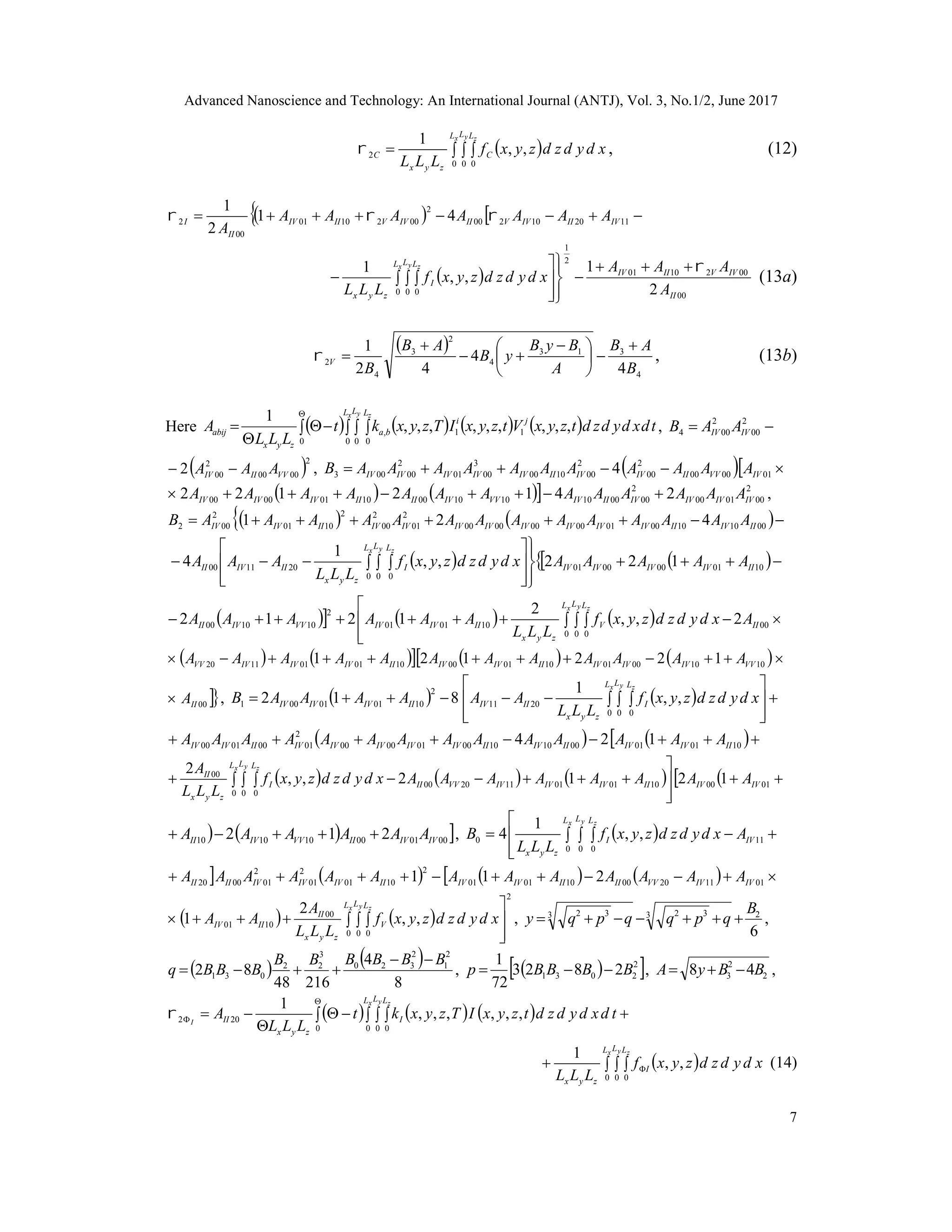
This paper presents a method to increase the density of field-effect transistors in inverter circuits by manufacturing a heterostructure with optimized dopant distribution through diffusion or ion implantation. It discusses how adjusting the dimensions and properties of integrated circuits can enhance performance and reliability using spatio-temporal models of dopant and defect concentrations. The analytical approach aids in optimizing the manufacturing process while accounting for the interactions between materials in the heterostructure.


