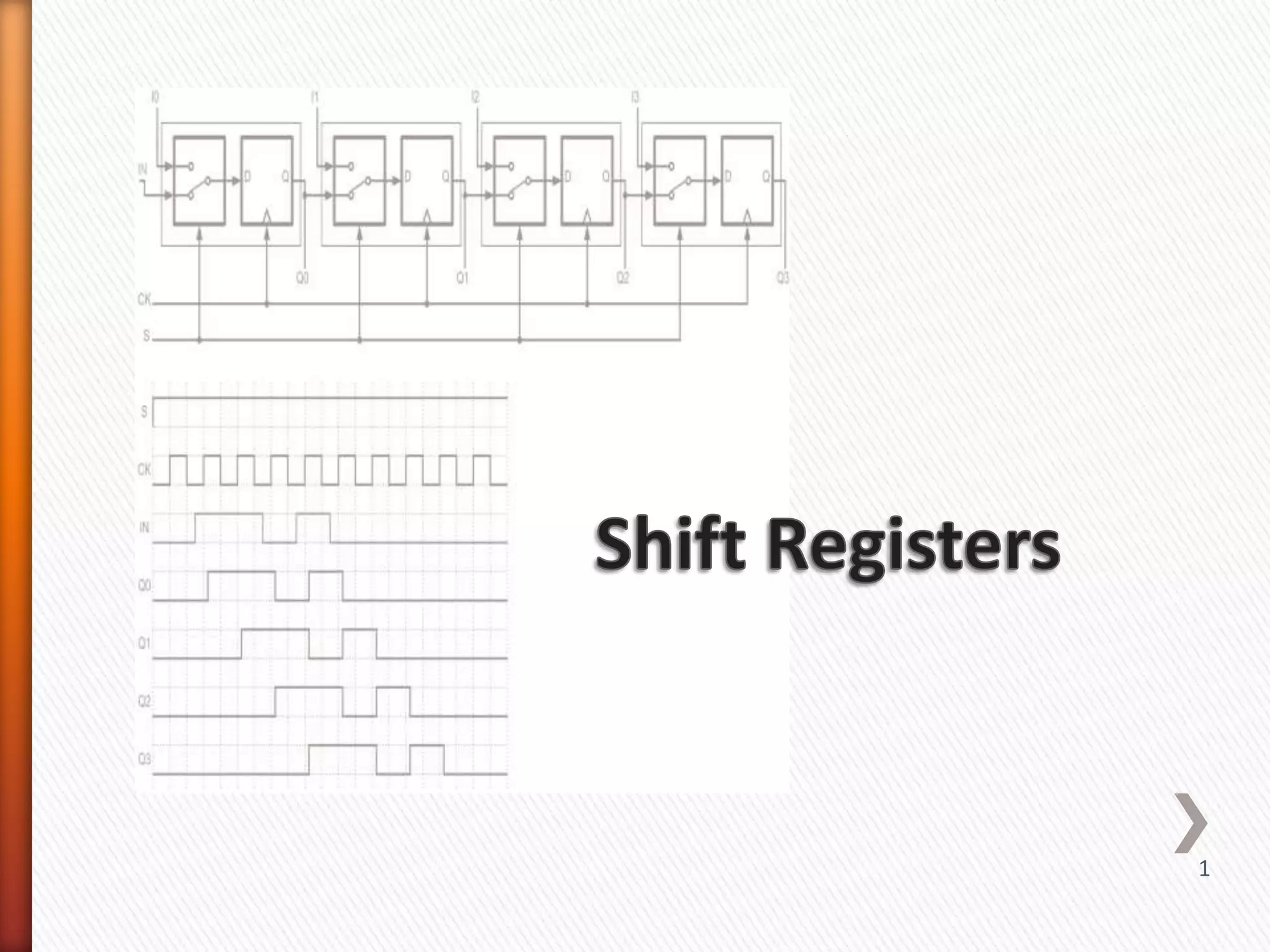
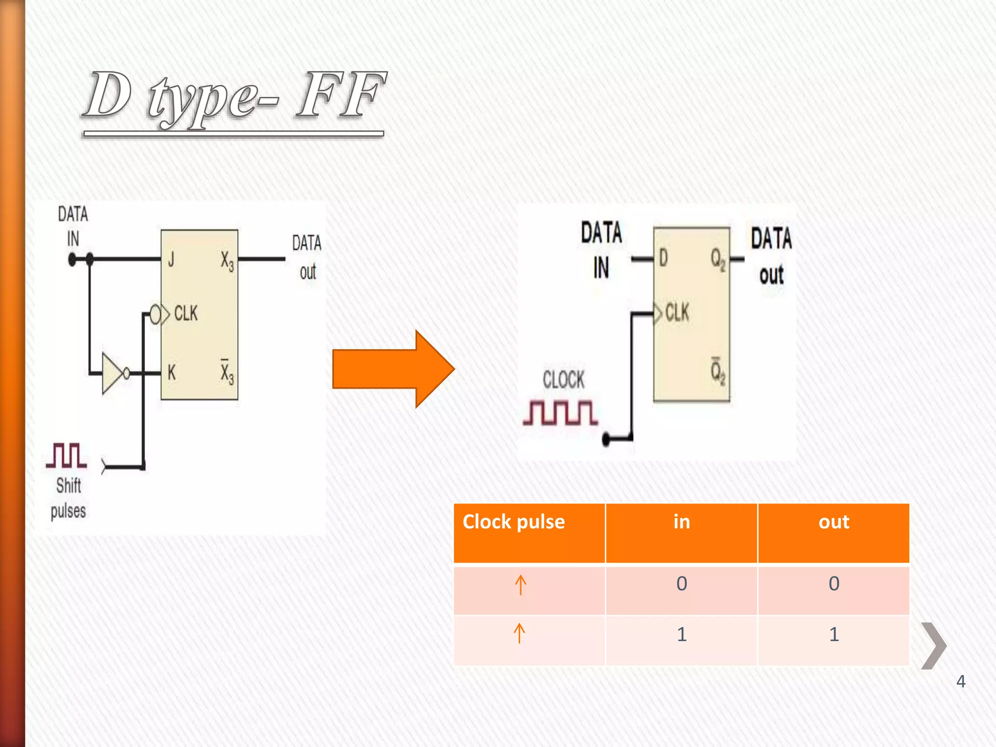
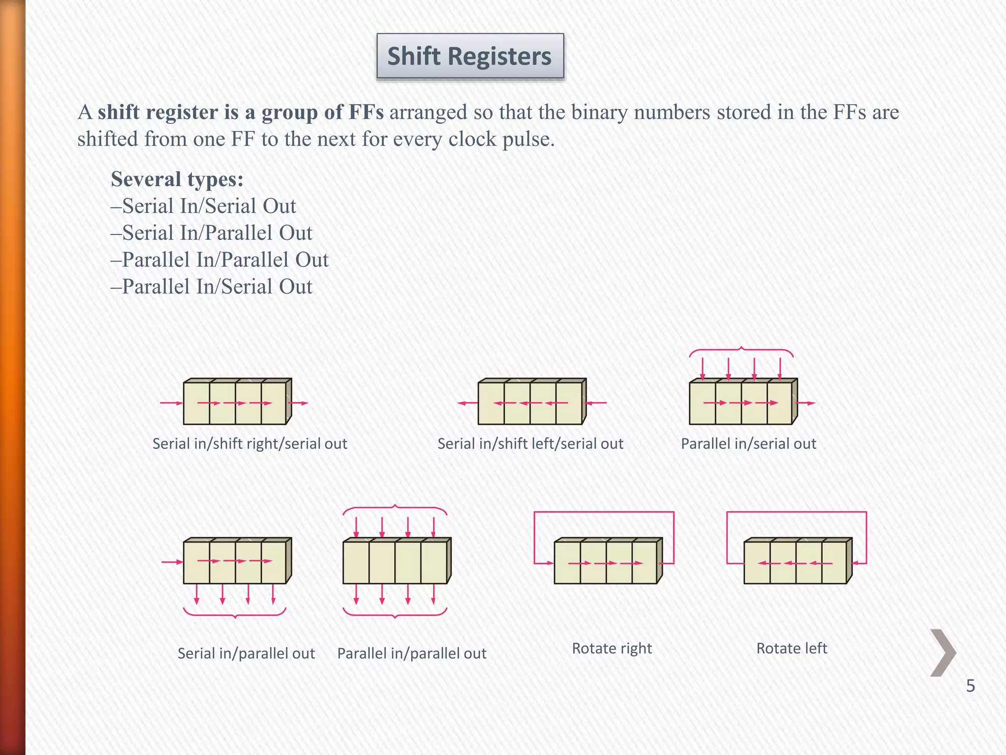
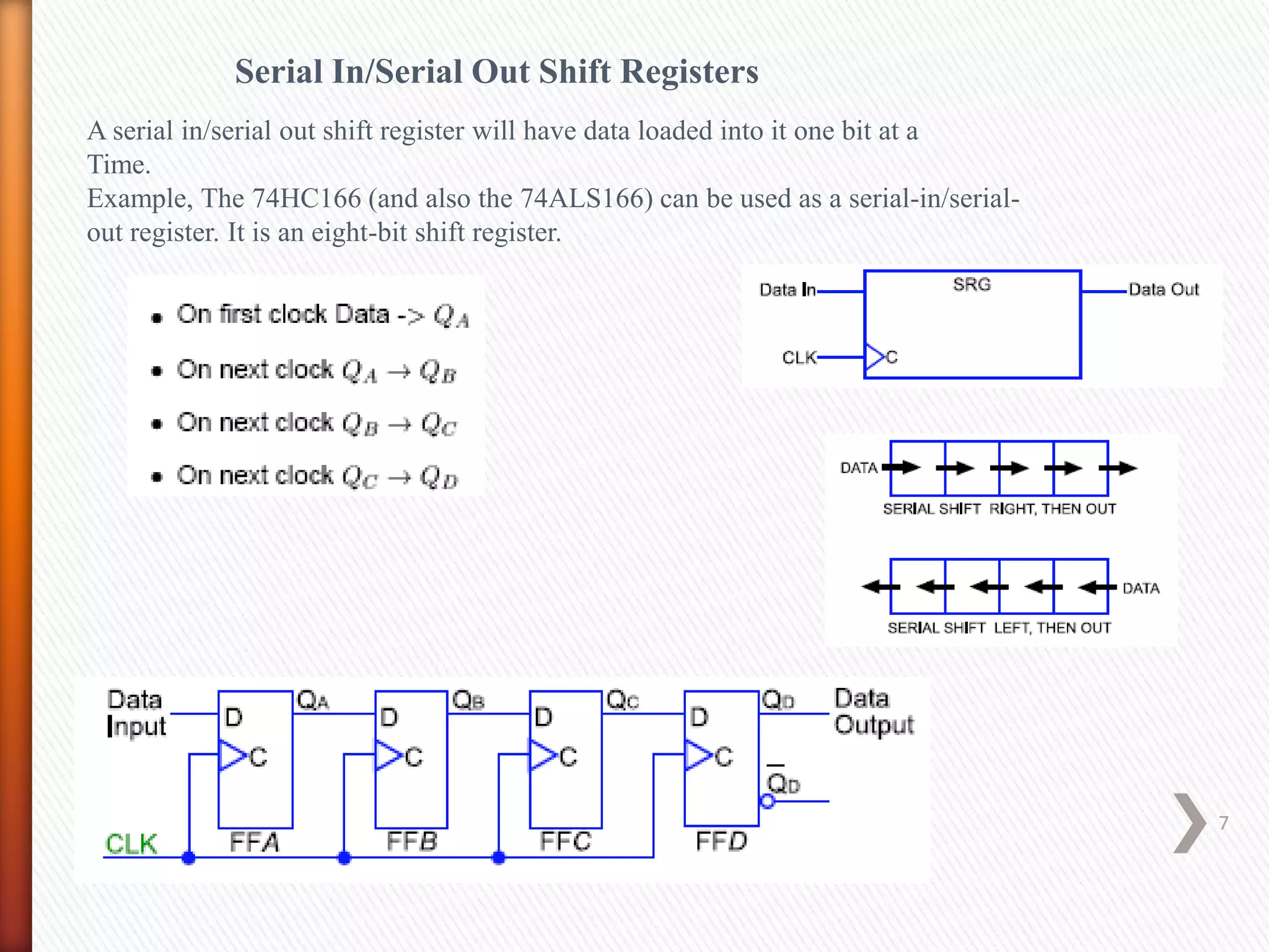
1. A shift register is a group of flip-flops arranged so that the binary numbers stored in the flip-flops are shifted from one flip-flop to the next for every clock pulse. There are several types including serial in/serial out, serial in/parallel out, parallel in/parallel out, and parallel in/serial out.
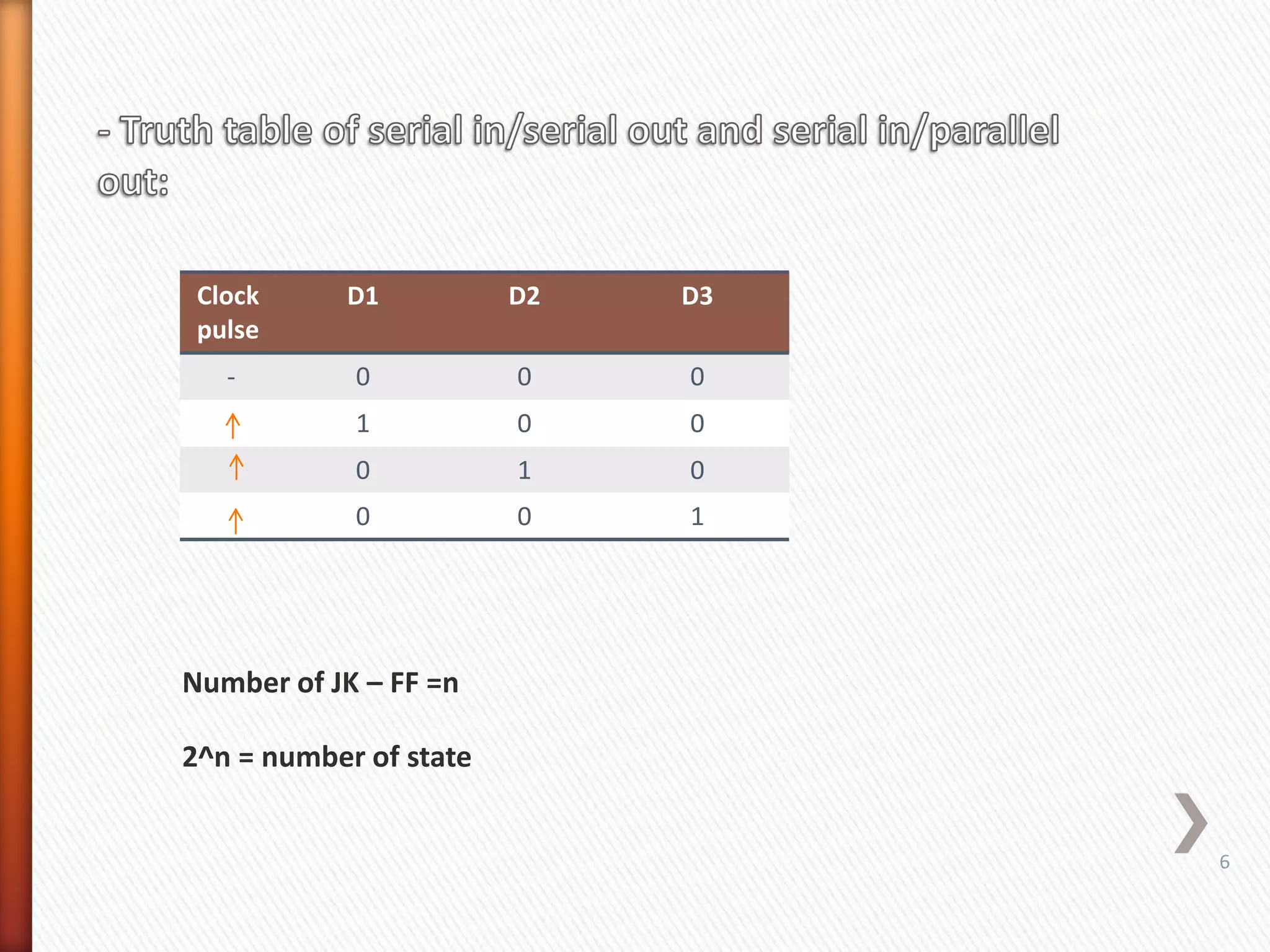
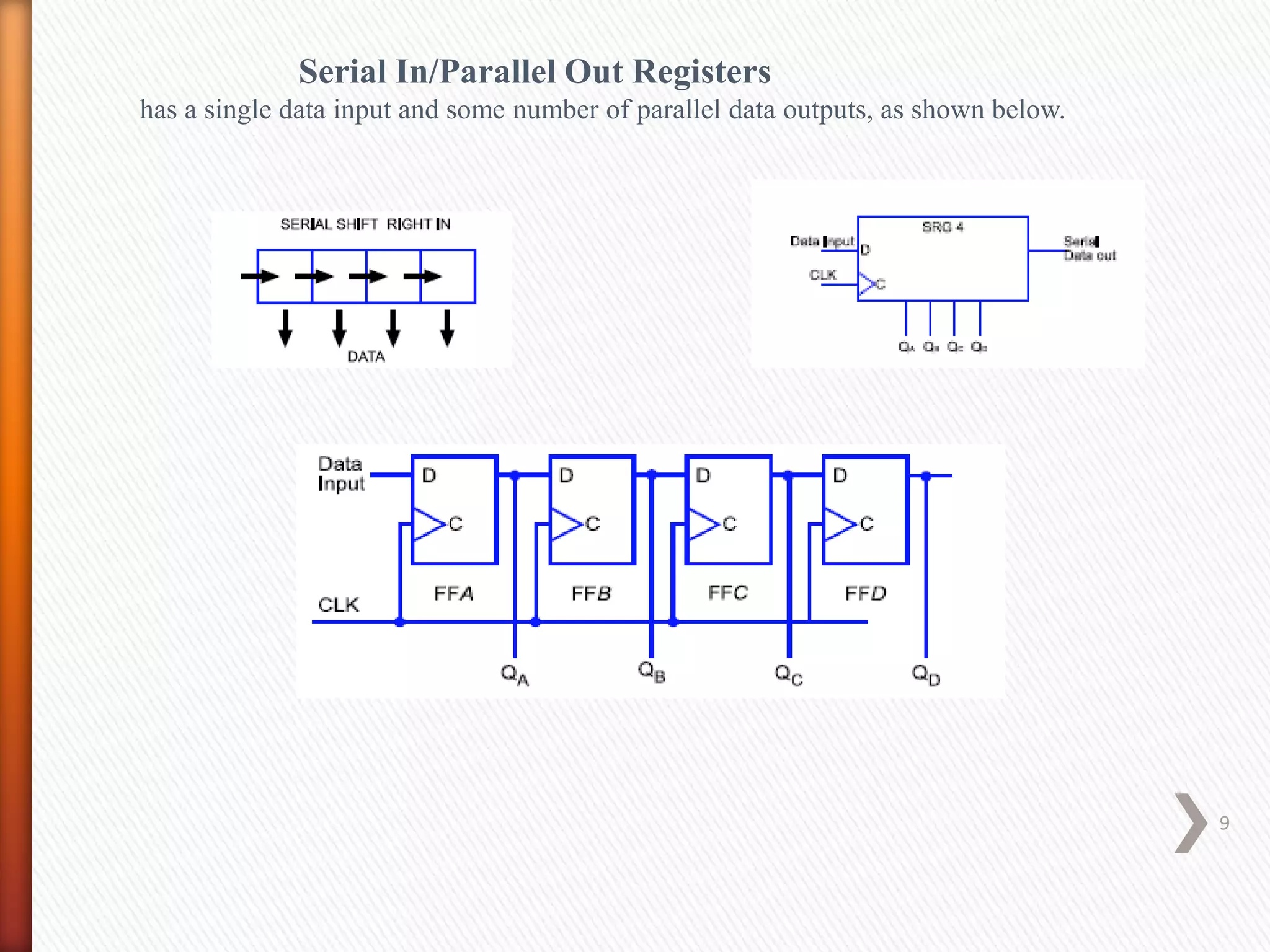
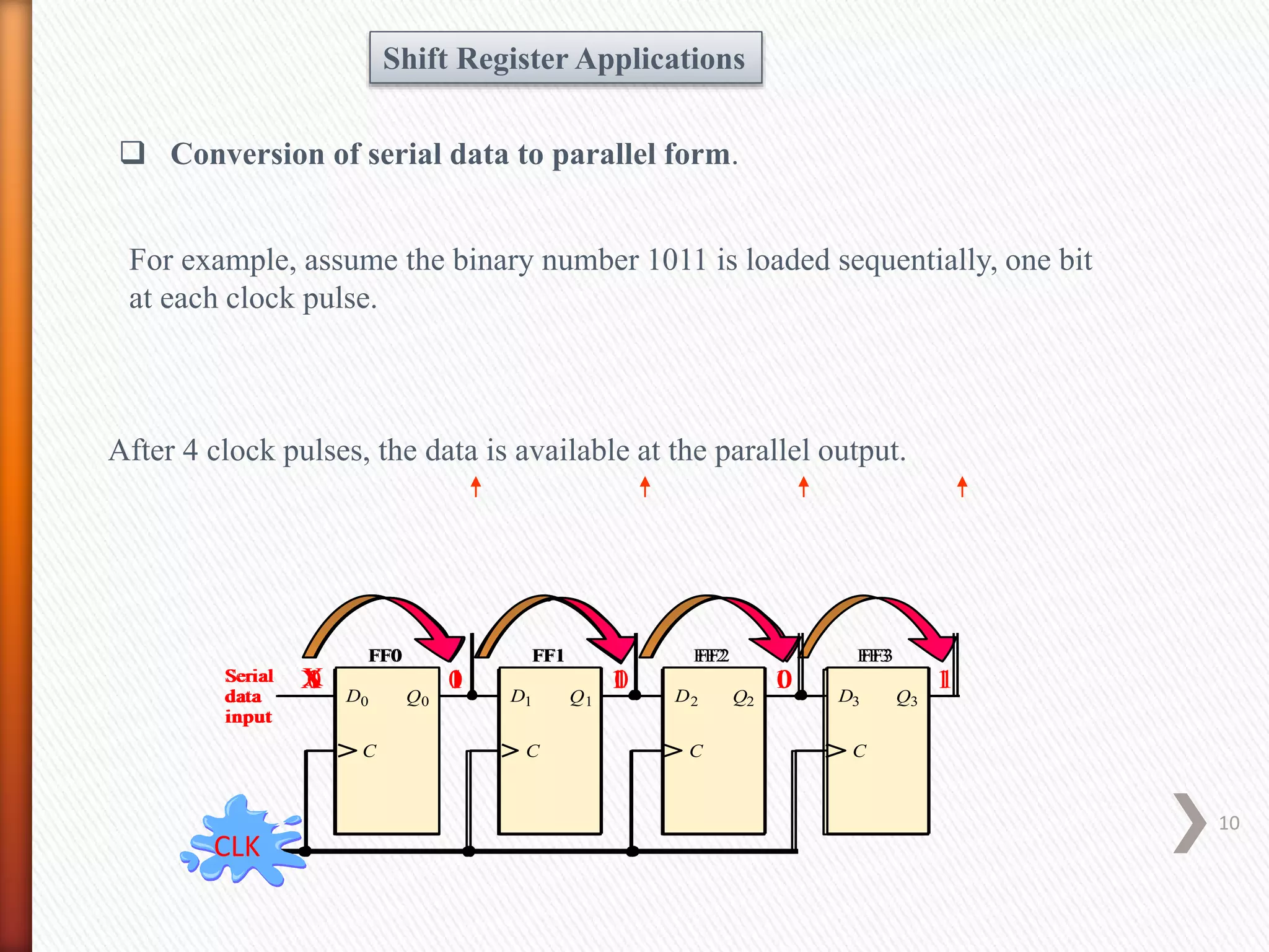
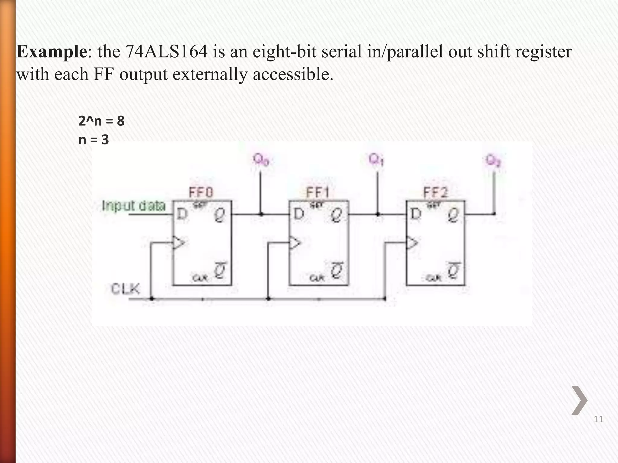
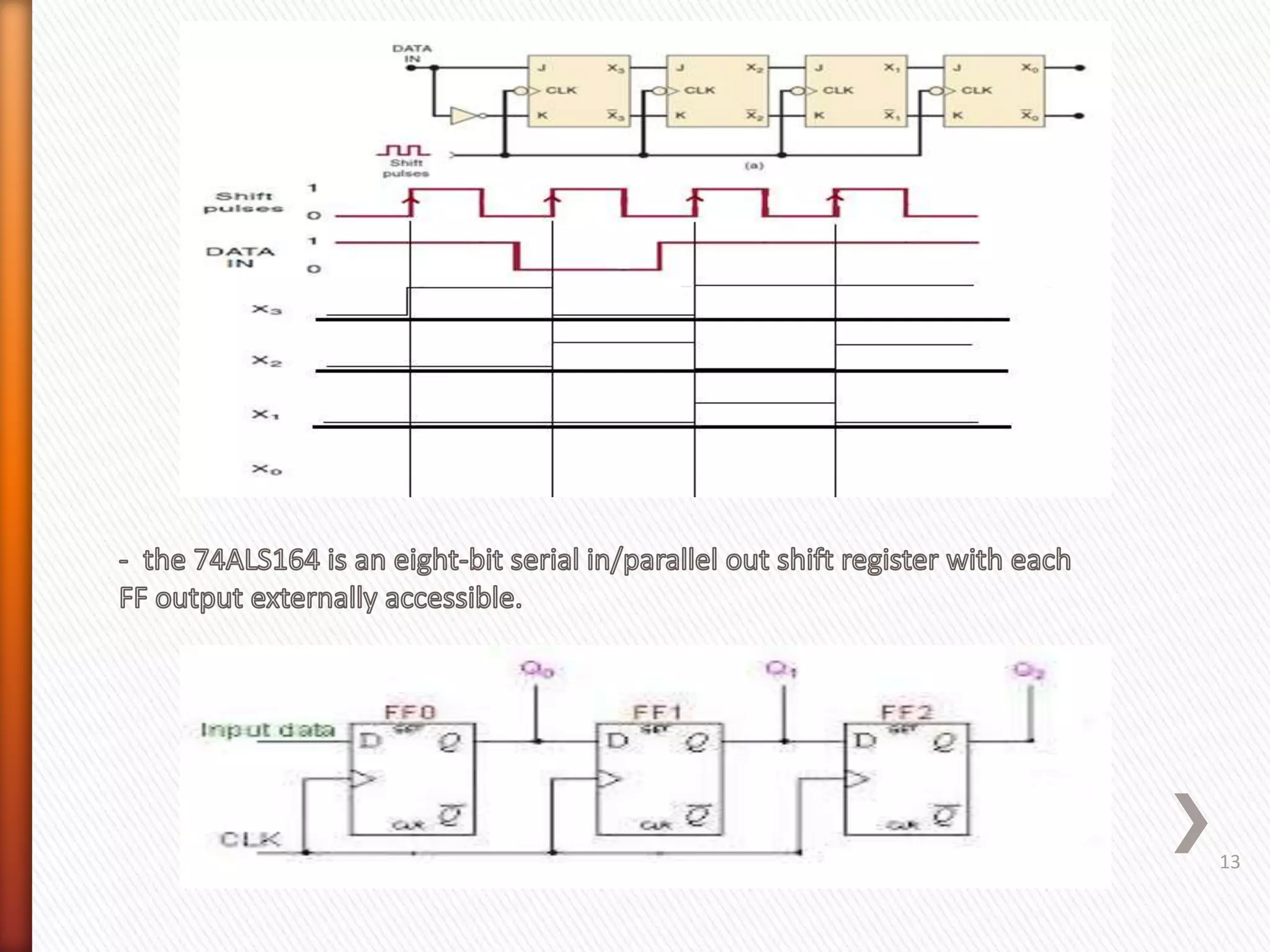
2. A serial in/parallel out shift register has a single data input and multiple parallel data outputs. It can be used to convert serial data to parallel form by loading data in one bit at a time over successive clock pulses until the full number is stored with its bits available at the outputs.
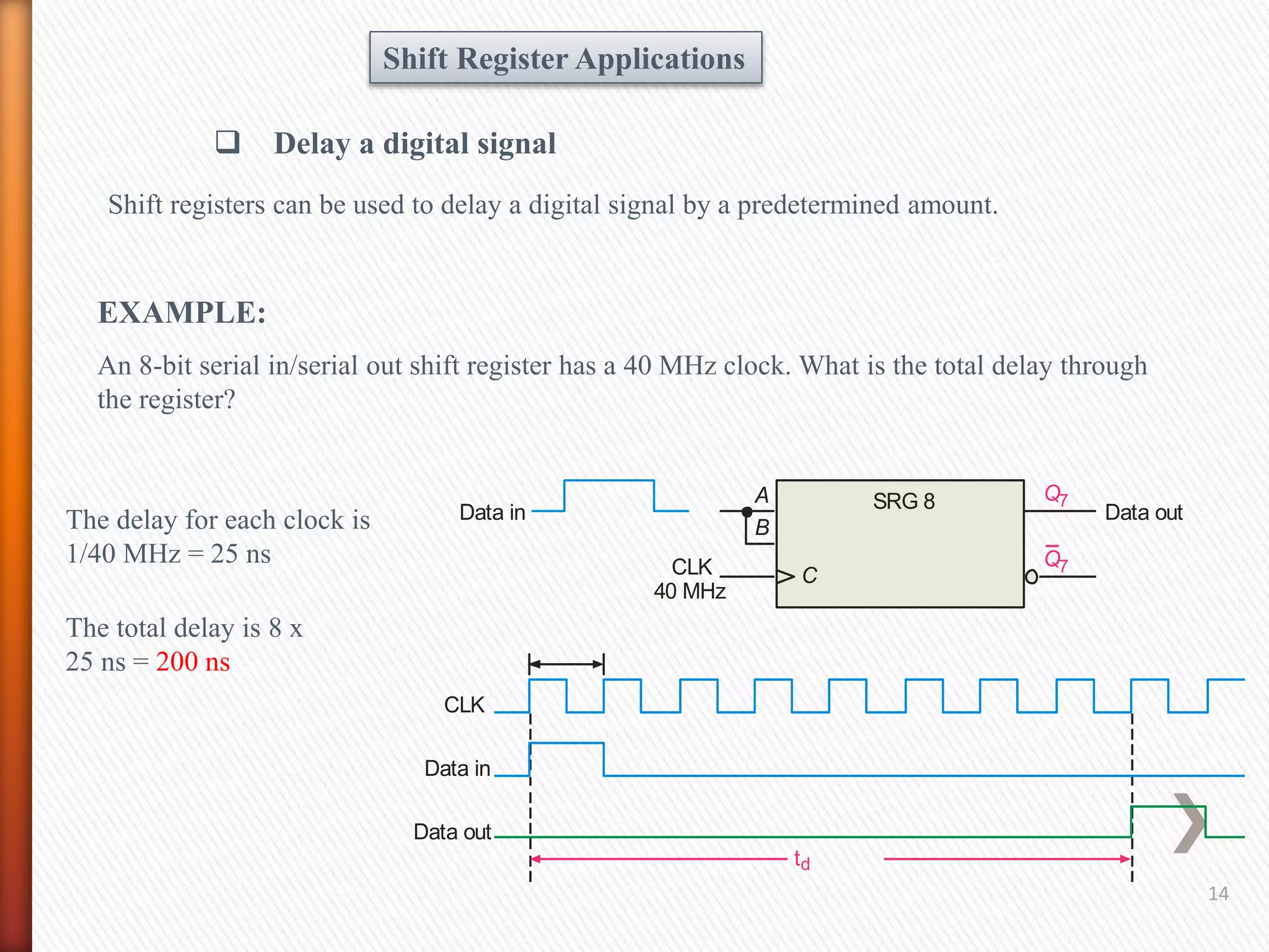
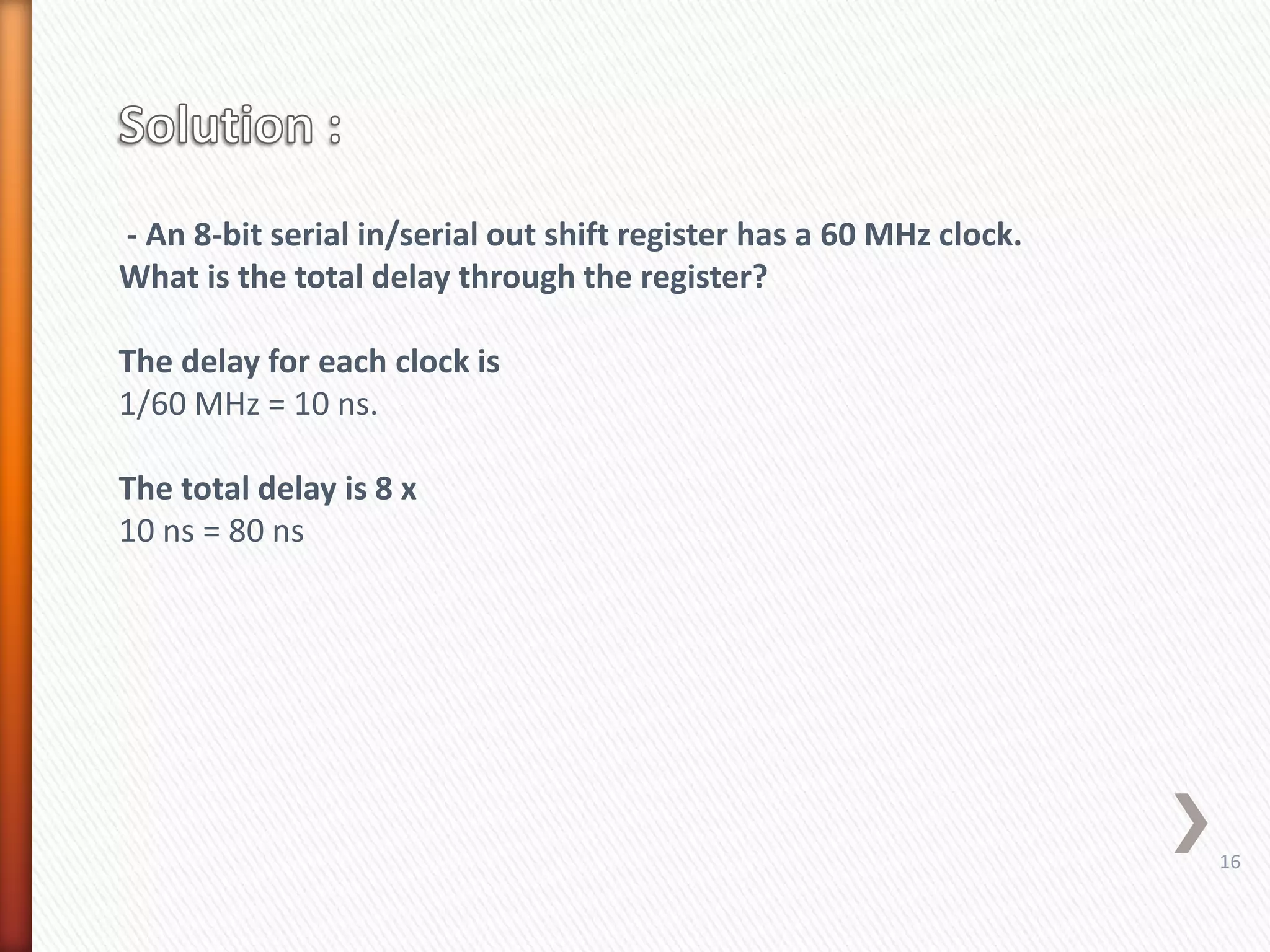
3. Shift registers can be used to delay a digital