Department of ComputerScience and Engg 1
By,
Dr. Ashwini N
Assistant Professor
Dept. of Information Science & Engineering
BMS Institute of Technology, Bengaluru.
Digital design and computer
organization
BCS302
Module 2
Combinational Circuits
2.
Department of ComputerScience and Engg
10/08/2025 2
Design Procedure
• From the specifications of the circuit determine the required number of
inputs and outputs and assign a symbol to each
• Derive the truth table that defines the required relationship between
inputs and outputs
• Obtain the specified Boolean functions for each output as a function of
the input variables
• Draw the logic diagram and verify the correctness of the design
Department of ComputerScience and Engg
6
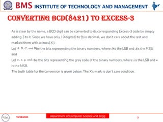
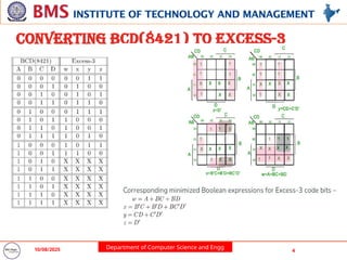
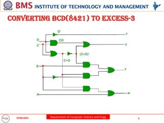
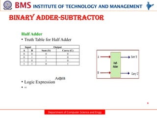
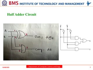
Half Adder
• Truth Table for Half Adder
• Logic Expression
• =
Input Output
A B Sum (S) Carry (C)
0 0 0 0
0 1 1 0
1 0 1 0
1 1 0 1
Binary Adder-Subtractor
Department of ComputerScience and Engg
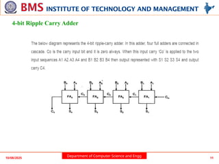
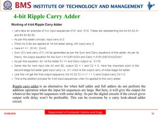
4-bit Ripple Carry Adder
Ripple carry adder is an alternative for when half adder and full adders do not perform the
addition operation when the input bit sequences are large. But here, it will give the output for
whatever the input bit sequences with some delay. As per the digital circuits if the circuit gives
output with delay won’t be preferable. This can be overcome by a carry look-ahead adder
circuit.
10/08/2025 12
13.
Department of ComputerScience and Engg
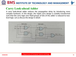
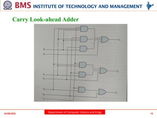
Carry Look-ahead Adder
A carry look-ahead adder reduces the propagation delay by introducing more
complex hardware. In this design, the ripple carry design is suitably transformed
such that the carry logic over fixed groups of bits of the adder is reduced to two-
level logic. Let us discuss the design in detail.
10/08/2025 13
14.
Department of ComputerScience and Engg
Carry Look-ahead Adder
The corresponding boolean expressions are given here to construct a carry look ahead adder.
In the carry-lookahead circuit we ned to generate the two signals carry propagator(P) and
carry generator(G),
Pi = Ai Bi
⊕
Gi = Ai · Bi
The output sum and carry can be expressed as
Si = Pi Ci
⊕
Ci+1 = Gi + ( Pi · Ci)
Boolean function for the carry output of each stage and substitute for each Ci its value from
the previous equations:
C0= input carry
C1 = G0 + P0 · C0
C2 = G1 + P1 · C1 = G1 + P1 · G0 + P1 · P0 · C0
C3 = G2 + P2 · C2 = G2 P2 · G1 + P2 · P1 · G0 + P2 · P1 · P0 · C0
10/08/2025 14
Department of ComputerScience and Engg 16
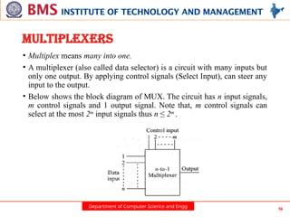
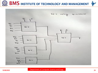
MULTIPLEXERS
• Multiplex means many into one.
• A multiplexer (also called data selector) is a circuit with many inputs but
only one output. By applying control signals (Select Input), can steer any
input to the output.
• Below shows the block diagram of MUX. The circuit has n input signals,
m control signals and 1 output signal. Note that, m control signals can
select at the most 2m
input signals thus n ≤ 2m
.
17.
Department of ComputerScience and Engg 17
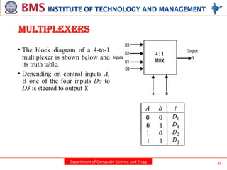
MULTIPLEXERS
• The block diagram of a 4-to-1
multiplexer is shown below and
its truth table.
• Depending on control inputs A,
B one of the four inputs Do to
D3 is steered to output Y.
18.
Department of ComputerScience and Engg 19
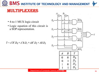
MULTIPLEXERS
• 4-to-1 MUX logic circuit
• Logic equation of this circuit is
a SOP representation.
19.
Department of ComputerScience and Engg 20
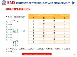
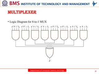
MULTIPLEXERS
• 8-to-1 multiplexer
Z = A′B′C′I0 + A′B′CI1 + A′BC′I2 + A′BCI3 + AB′C′I4 + AB′CI5 + ABC′I6
+ ABCI7
Select/Control Input Output
A B C Z
0 0 0 I0
0 0 1 I1
0 1 0 I2
0 1 1 I3
1 0 0 I4
1 0 1 I5
1 1 0 I6
1 1 1 I7
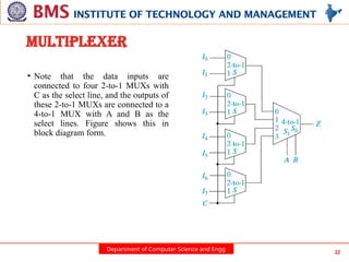
Department of ComputerScience and Engg 22
MULTIPLEXER
• Note that the data inputs are
connected to four 2-to-1 MUXs with
C as the select line, and the outputs of
these 2-to-1 MUXs are connected to a
4-to-1 MUX with A and B as the
select lines. Figure shows this in
block diagram form.
22.
Department of ComputerScience and Engg 23
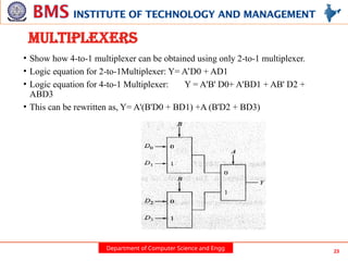
MULTIPLEXERS
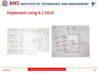
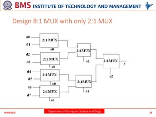
• Show how 4-to-1 multiplexer can be obtained using only 2-to-1 multiplexer.
• Logic equation for 2-to-1Multiplexer: Y= A’D0 + AD1
• Logic equation for 4-to-1 Multiplexer: Y = A'B' D0+ A'BD1 + AB' D2 +
ABD3
• This can be rewritten as, Y= A'(B'D0 + BD1) +A (B'D2 + BD3)
Department of ComputerScience and Engg
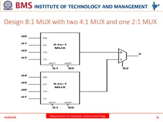
Design 8:1 MUX with two 4:1 MUX and one 2:1 MUX
10/08/2025 26
26.
Department of ComputerScience and Engg 27
MULTIPLEXERS
• Realize Y=A'B + B'C' + ABC using an 8-to-1 multiplexer.
• First we express Y as a function of minterms of three variables. Thus
• Y = A'B + B'C' + ABC
• Y =A'B(C' + C)+B'C'(A' + A)+ ABC [As,X+X'= I]
• Y = A'B'C' + A'BC' + A'BC + AB'C' + ABC
• Comparing this with equation of 8 to 1 multiplexer, we find by
substituting D0 = D2 = D3 =D4 = D7 = 1 and D1 = D5 = D6 = 0.
27.
Department of ComputerScience and Engg 28
MULTIPLEXERS
• Can it be realized Y =A'B + B'C‘ + ABC equation with a 4-to-1
multiplexer?
• The 4-to-1 multiplexer generates 4 minterms for different
combinations of AB. We rewrite given logic equation in such a way
that all these terms are present in the equation.
• Y =A'B+B'C' +ABC
• Y =A'B+ B'C'(A' +A)+ ABC [As,X +X' = I]
• Y =A'B'.C' + A'B.1 +AB'.C' + AB.C
• Compare above with equation of a 4-to-1 multiplexer. We see D0= C',
D1 = 1, D2 = C' and D3 = C generate the given logic function.
28.
Department of ComputerScience and Engg 29
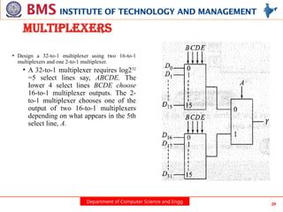
MULTIPLEXERS
• Design a 32-to-1 multiplexer using two 16-to-1
multiplexers and one 2-to-1 multiplexer.
• A 32-to-1 multiplexer requires log232
=5 select lines say, ABCDE. The
Iower 4 select lines BCDE choose
16-to-1 multiplexer outputs. The 2-
to-1 multiplexer chooses one of the
output of two 16-to-1 multiplexers
depending on what appears in the 5th
select line, A.
Department of ComputerScience and Engg
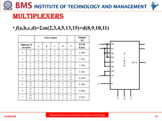
• f(a,b,c,d)=Σm(2,3,4,5,13,15)+d(8,9,10,11)
10/08/2025 31
MULTIPLEXERS
D0
D1
D2
D3
D4
D5
D6
D7
0
1
d
E
0
a b c
05,Y Y
8
:
1
M
U
X
Department of ComputerScience and Engg 33
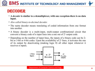
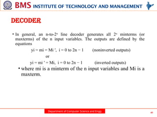
DECODER
• A decoder is similar to a demultiplexer, with one exception-there is no data
input.
• Also called binary-to-decimal decoder.
• The name decoder means translating of coded information from one format
into another.
• A binary decoder is a multi-input, multi-output combinational circuit that
converts a binary code of n input lines into a one out of 2n
output code.
• Depending on the number of input lines, the inputs of a binary code can be 2-
bit or 3-bit or 4-bit codes. Upon the availability of 2n
lines, it activates the one
of its output by deactivating (making logic 0) all other input whenever it
receives n inputs.
33.
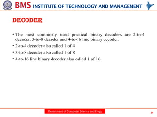
Department of ComputerScience and Engg 34
DECODER
• The most commonly used practical binary decoders are 2-to-4
decoder, 3-to-8 decoder and 4-to-16 line binary decoder.
• 2-to-4 decoder also called 1 of 4
• 3-to-8 decoder also called 1 of 8
• 4-to-16 line binary decoder also called 1 of 16
34.
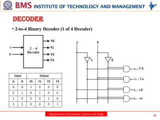
Department of ComputerScience and Engg 35
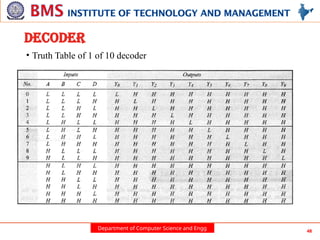
DECODER
• 2-to-4 Binary Decoder (1 of 4 Decoder)
Input Output
A B Y0 Y1 Y2 Y3
0 0 1 0 0 0
0 1 0 1 0 0
1 0 0 0 1 0
1 1 0 0 0 1
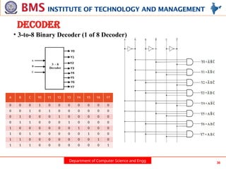
Department of ComputerScience and Engg 37
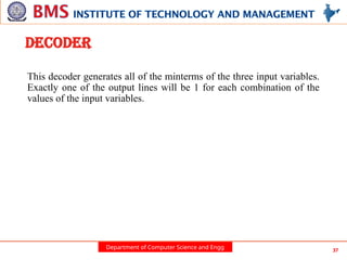
DECODER
This decoder generates all of the minterms of the three input variables.
Exactly one of the output lines will be 1 for each combination of the
values of the input variables.
Department of ComputerScience and Engg 40
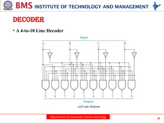
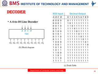
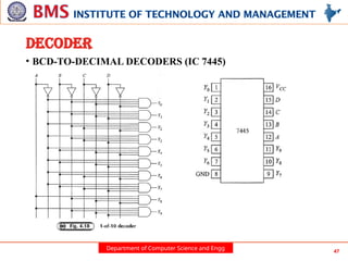
DECODER
• A 4-to-10 Line Decoder
• This decoder has inverted outputs (indicated by the small circles).
• For each combination of the values of the inputs, exactly one of the output lines
will be 0.
• When a binary-coded-decimal (BCD) digit is used as an input to this
decoder, one of the output lines will go low to indicate which of the
10 decimal digits is present.
40.
Department of ComputerScience and Engg 41
DECODER
• In general, an n-to-2n
line decoder generates all 2n
minterms (or
maxterms) of the n input variables. The outputs are defined by the
equations
yi = mi = Mi ′, i = 0 to 2n − 1 (noninverted outputs)
or
yi = mi ′ = Mi, i = 0 to 2n − 1 (inverted outputs)
• where mi is a minterm of the n input variables and Mi is a
maxterm.
41.
Department of ComputerScience and Engg 42
DECODER
Applications of Decoders
Decoders are greatly used in applications where the particular output or group of outputs to be activated
only on the occurrence of a specific combination of input levels.
• Binary to Decimal Decoder
Decoders are used to get the decimal digit corresponding to a specific input combination. A BCD
number needs 4 binary digits to represent the 0 to 9 decimal digits, thus it consists of 4 input lines. It
consists of 10 output lines corresponding to 0 to 9 decimal digits. (1 of 10 line decoder)
• Address Decoders
Amongst its many uses, a decoder is widely used to decode the particular memory location in the
computer memory system. Decoders accept the address code generated by the CPU which is a
combination of address bits for a specific location in the memory. In a memory system, there are
several memory ICs are combined and each one has their unique address to distinguish from other
memory locations. In such cases a decoder built in the memory ICs circuitry, is used to select a
memory IC in response to a range of addresses by decoding the most significant bits of the systems
address, thereby a particular memory location or IC is selected.
• Instruction Decoder
Another application of the decoder can be found in the control unit of the central processing unit.
This decoder is used to decode the program instructions in order to activate the specific control lines
such that different operations in the ALU of the CPU are carried out.
42.
Department of ComputerScience and Engg 43
DECODER
• Because an n-input decoder generates all of the minterms of n
variables, n- variable functions can be realized by ORing together
selected minterm outputs from a decoder.
• If the decoder outputs are inverted, then NAND gates can be used to
generate the functions.
43.
Department of ComputerScience and Engg 44
DECODER
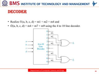
• Realize f1(a, b, c, d) = m1 + m2 + m4 and
• f2(a, b, c, d) = m4 + m7 + m9 using the 4 to 10 line decoder.
44.
Department of ComputerScience and Engg 45
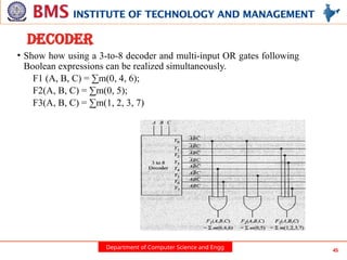
DECODER
• Show how using a 3-to-8 decoder and multi-input OR gates following
Boolean expressions can be realized simultaneously.
F1 (A, B, C) = ∑m(0, 4, 6);
F2(A, B, C) = ∑m(0, 5);
F3(A, B, C) = ∑m(1, 2, 3, 7)
45.
Department of ComputerScience and Engg 46
DECODER
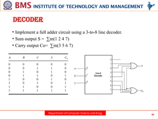
• Implement a full adder circuit using a 3-to-8 line decoder.
• Sum output S = ∑m(1 2 4 7)
• Carry output Co= ∑m(3 5 6 7)
Department of ComputerScience and Engg 49
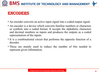
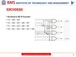
ENCODERS
• An encoder converts an active input signal into a coded output signal.
• An encoder is a device which converts familiar numbers or characters
or symbols into a coded format. It accepts the alphabetic characters
and decimal numbers as inputs and produces the outputs as a coded
representation of the inputs.
• It is a combinational circuit that performs the opposite function of a
decoder.
• These are mainly used to reduce the number of bits needed to
represent given information.
49.
Department of ComputerScience and Engg 50
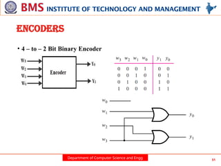
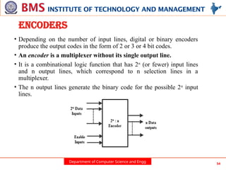
ENCODERS
• Depending on the number of input lines, digital or binary encoders
produce the output codes in the form of 2 or 3 or 4 bit codes.
• An encoder is a multiplexer without its single output line.
• It is a combinational logic function that has 2n
(or fewer) input lines
and n output lines, which correspond to n selection lines in a
multiplexer.
• The n output lines generate the binary code for the possible 2n
input
lines.
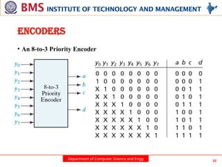
Department of ComputerScience and Engg 53
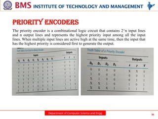
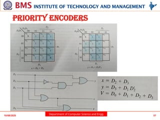
ENCODERS
• An 8-to-3 Priority Encoder
• 8-to-3 priority encoder with inputs y0 through y7.
• If input yi is 1 and the other inputs are 0, then the abc outputs represent a binary
number equal to i.
• For example, if y3 = 1, then abc = 011.
• If more than one input can be 1 at the same time, the output can be defined using a
priority scheme.
• The truth table uses the following scheme:
• If more than one input is 1, the highest numbered input determines the
output.
• For example, if inputs y1, y4, and y5 are 1, the output is abc = 101.
• The X’s in the table are don’t-cares; for example, if y5 is 1, we do not
care what inputs y0 through y4 are.
• Output d is 1 if any input is 1, otherwise, d is 0.
• This signal is needed to distinguish the case of all 0 inputs from the case where only y0 is 1.
53.
Department of ComputerScience and Engg 54
ENCODERS
• Depending on the number of input lines, digital or binary encoders
produce the output codes in the form of 2 or 3 or 4 bit codes.
• An encoder is a multiplexer without its single output line.
• It is a combinational logic function that has 2n
(or fewer) input lines
and n output lines, which correspond to n selection lines in a
multiplexer.
• The n output lines generate the binary code for the possible 2n
input
lines.
Department of ComputerScience and Engg 56
Priority ENCODERS
The priority encoder is a combinational logic circuit that contains 2^n input lines
and n output lines and represents the highest priority input among all the input
lines. When multiple input lines are active high at the same time, then the input that
has the highest priority is considered first to generate the output.
Department of ComputerScience and Engg 58
ENCODERS
• An 8-to-3 Priority Encoder
• 8-to-3 priority encoder with inputs y0 through y7.
• If input yi is 1 and the other inputs are 0, then the abc outputs represent a binary
number equal to i.
• For example, if y3 = 1, then abc = 011.
• If more than one input can be 1 at the same time, the output can be defined using a
priority scheme.
• The truth table uses the following scheme:
• If more than one input is 1, the highest numbered input determines the
output.
• For example, if inputs y1, y4, and y5 are 1, the output is abc = 101.
• The X’s in the table are don’t-cares; for example, if y5 is 1, we do not
care what inputs y0 through y4 are.
• Output d is 1 if any input is 1, otherwise, d is 0.
• This signal is needed to distinguish the case of all 0 inputs from the case where only y0 is 1.
Department of ComputerScience and Engg 61
Introduction to latches and flipflops
• Sequential switching circuits have the property that the output
depends not only on the present input but also on the past sequence of
inputs.
• In effect, these circuits must be able to “remember” something about
the past history of the inputs in order to produce the present output.
• Latches and flip-flops are commonly used memory devices in
sequential circuits.
• A memory element that has no clock input is often called a latch.
• A memory element that has clock input is often called a Flip-Flop.
A flip-flop is a bi stable electronic circuit that has 2 stable state
i.e. output is either logic 0 or logic 1
Department of ComputerScience and Engg
10/08/2025 63
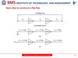
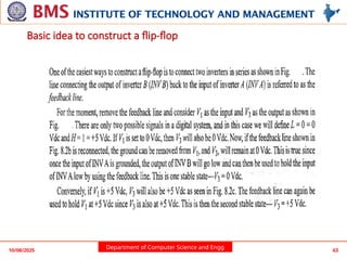
Basic idea to construct a flip-flop
63.
Department of ComputerScience and Engg 64
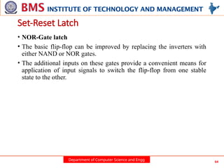
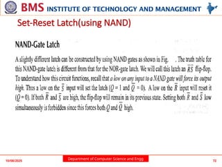
Set-Reset Latch
• NOR-Gate latch
• The basic flip-flop can be improved by replacing the inverters with
either NAND or NOR gates.
• The additional inputs on these gates provide a convenient means for
application of input signals to switch the flip-flop from one stable
state to the other.
64.
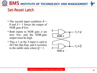
Department of ComputerScience and Engg 65
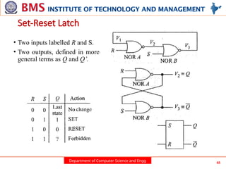
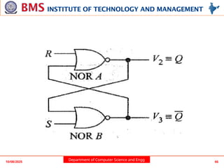
• Two inputs labelled R and S.
• Two outputs, defined in more
general terms as Q and Q’.
Set-Reset Latch
Department of ComputerScience and Engg 67
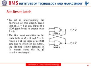
• To aid in understanding the
operation of this circuit, recall
that an H = 1 at any input of a
NOR gate forces its output to an
L = 0.
• The first input condition in the
truth table is R = 0 and S = 0.
Since a 0 at the input of a NOR
gate has no effect on its output,
the flip-flop simply remains in
its present state; that is, Q
remains unchanged.
Set-Reset Latch
67.
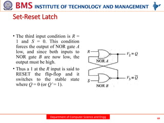
Department of ComputerScience and Engg 68
• The second input condition R =
0 and S = 1 forces the output of
NOR gate B low.
• Both inputs to NOR gate A are
now low, and the NOR-gate
output must be high.
• Thus a 1 at the S input is said to
SET the flip-flop, and it switches
to the stable state where Q = 1.
Set-Reset Latch
68.
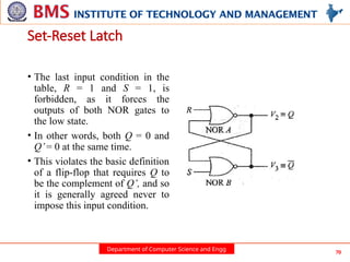
Department of ComputerScience and Engg 69
• The third input condition is R =
1 and S = 0. This condition
forces the output of NOR gate A
low, and since both inputs to
NOR gate B are now low, the
output must be high.
• Thus a 1 at the R input is said to
RESET the flip-flop and it
switches to the stable state
where Q = 0 (or Q’= 1).
Set-Reset Latch
69.
Department of ComputerScience and Engg 70
• The last input condition in the
table, R = 1 and S = 1, is
forbidden, as it forces the
outputs of both NOR gates to
the low state.
• In other words, both Q = 0 and
Q’= 0 at the same time.
• This violates the basic definition
of a flip-flop that requires Q to
be the complement of Q’, and so
it is generally agreed never to
impose this input condition.
Set-Reset Latch
Department of ComputerScience and Engg
10/08/2025 82
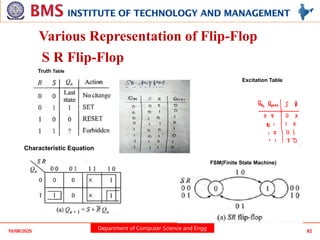
Various Representation of Flip-Flop
S R Flip-Flop
Truth Table
Characteristic Equation
Excitation Table
FSM(Finite State Machine)
82.
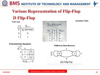
Department of ComputerScience and Engg
10/08/2025 83
Various Representation of Flip-Flop
D Flip-Flop
Truth Table
Characteristic Equation
Excitation Table
FSM(Finite State Machine)
83.
Department of ComputerScience and Engg
10/08/2025 84
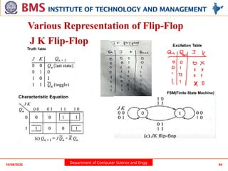
Various Representation of Flip-Flop
J K Flip-Flop
Truth Table
Characteristic Equation
Excitation Table
FSM(Finite State Machine)
84.
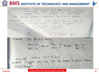
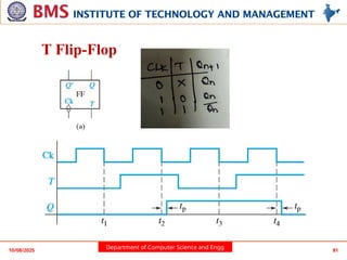
Department of ComputerScience and Engg
10/08/2025 85
Various Representation of Flip-Flop
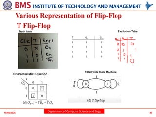
T Flip-Flop
Truth Table
Characteristic Equation
Excitation Table
FSM(Finite State Machine)
85.
Department of ComputerScience and Engg
VHDL codes of MUX, Binary
adders must be studied from Lab
session
10/08/2025 86
![Department of Computer Science and Engg 27
MULTIPLEXERS
• Realize Y=A'B + B'C' + ABC using an 8-to-1 multiplexer.
• First we express Y as a function of minterms of three variables. Thus
• Y = A'B + B'C' + ABC
• Y =A'B(C' + C)+B'C'(A' + A)+ ABC [As,X+X'= I]
• Y = A'B'C' + A'BC' + A'BC + AB'C' + ABC
• Comparing this with equation of 8 to 1 multiplexer, we find by
substituting D0 = D2 = D3 =D4 = D7 = 1 and D1 = D5 = D6 = 0.](https://image.slidesharecdn.com/module2ddcofinal-251008131741-effb4ae3/85/Module2_DDCO_Final-pptx-26-320.jpg)
![Department of Computer Science and Engg 28
MULTIPLEXERS
• Can it be realized Y =A'B + B'C‘ + ABC equation with a 4-to-1
multiplexer?
• The 4-to-1 multiplexer generates 4 minterms for different
combinations of AB. We rewrite given logic equation in such a way
that all these terms are present in the equation.
• Y =A'B+B'C' +ABC
• Y =A'B+ B'C'(A' +A)+ ABC [As,X +X' = I]
• Y =A'B'.C' + A'B.1 +AB'.C' + AB.C
• Compare above with equation of a 4-to-1 multiplexer. We see D0= C',
D1 = 1, D2 = C' and D3 = C generate the given logic function.](https://image.slidesharecdn.com/module2ddcofinal-251008131741-effb4ae3/85/Module2_DDCO_Final-pptx-27-320.jpg)