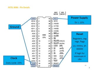
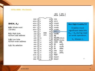
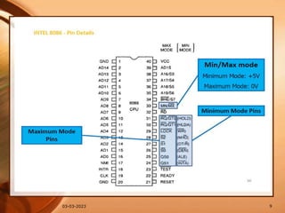
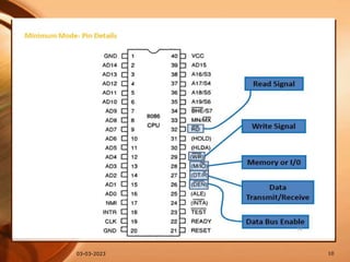
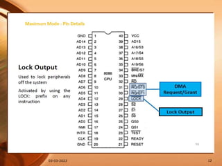
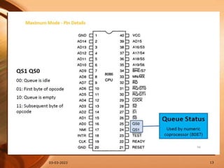
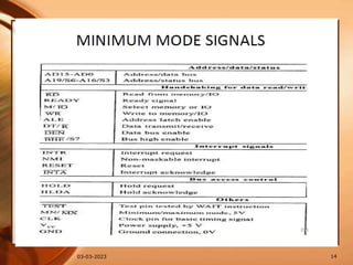
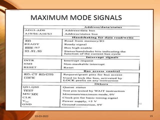
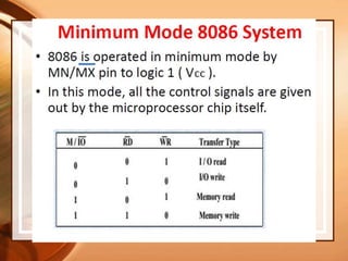
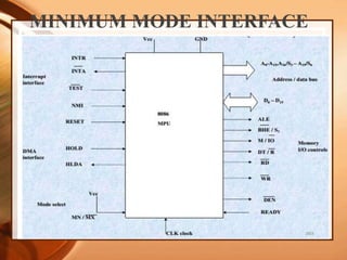
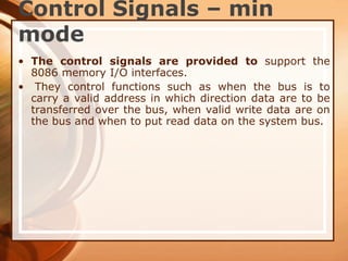
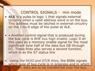
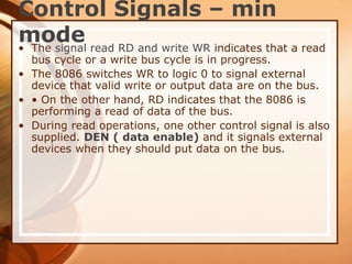
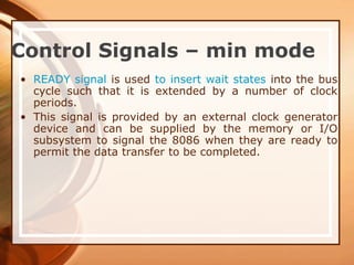
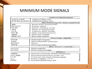
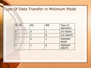
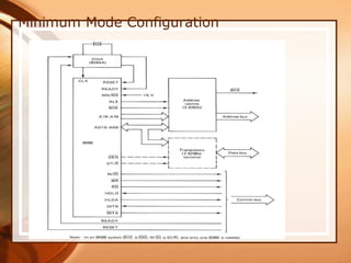
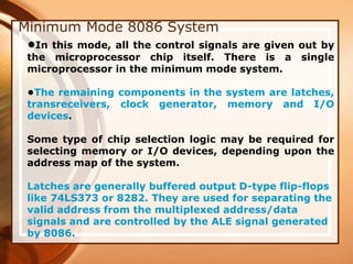
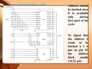
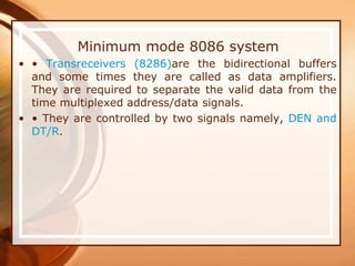
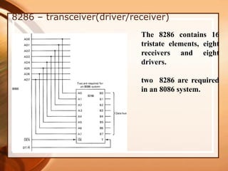
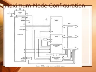
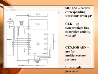
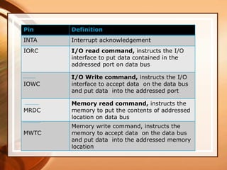
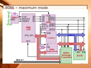
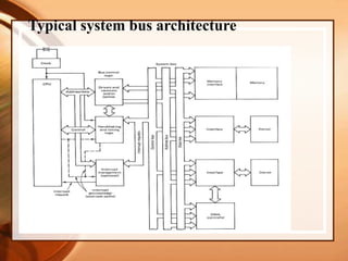
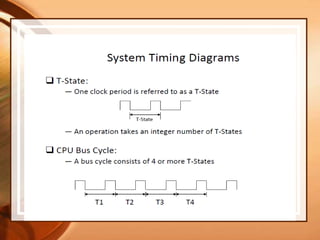
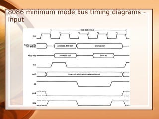
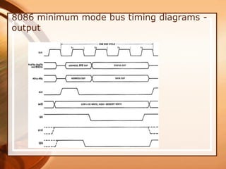
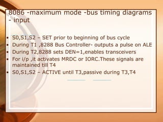
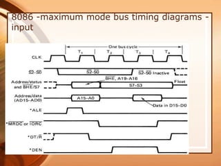
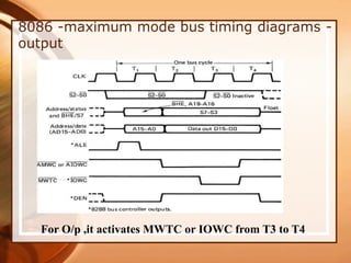
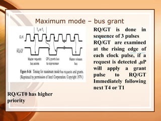
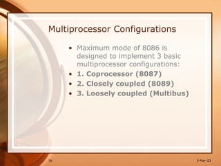
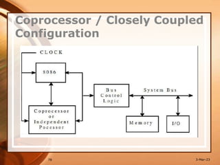
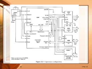
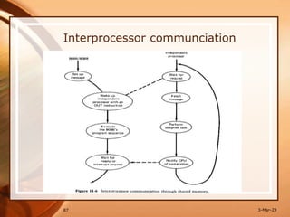
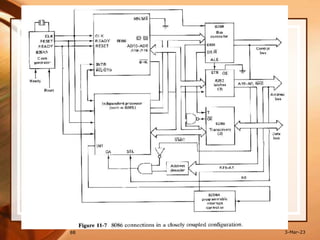
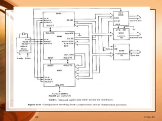
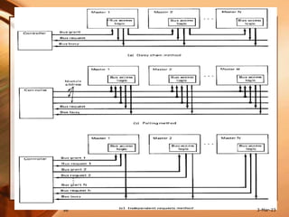
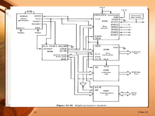
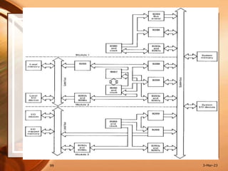
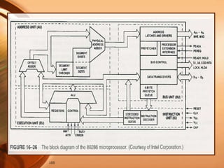
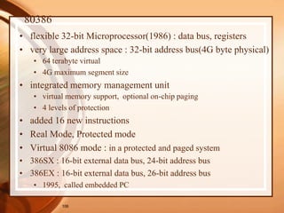
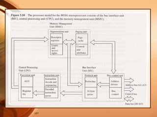
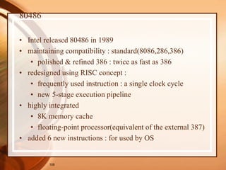
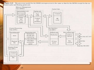
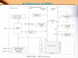
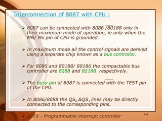
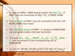
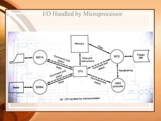
The document discusses the bus structure of the 8086 microprocessor system. It describes the minimum and maximum mode configurations of the 8086. In minimum mode, the 8086 provides all control signals for memory and I/O interfacing. It details the various address, data, status, control and interrupt signals involved. Maximum mode allows for multiprocessor systems by providing additional signals for bus arbitration and shared resources. The timing diagrams of typical read and write cycles are shown for both modes. Coprocessor and closely coupled multiprocessor configurations using the 8086 are also explained.


![ Depending on the data type handled these are
further grouped into Three :
Floating point Data Transfer
Integer Data Transfer
BCD Data Transfer
Floating Point Data Transfer
1. FLD (Load real to top of Stack)
This instruction loads a real operand to the
top of stack of the 80 bit register.
FLD ST (7) ; Stack top [Reg 7]
FLD MEM ; Stack Top [MEM]
151
1) Data Transfer Instruction](https://image.slidesharecdn.com/14004405-230303024548-aadd3c84/85/8086-Programing-ppt-151-320.jpg)
![152
2) FST (Store Top of the Operand )
This instruction stores current content of the top of stack
register to the specified operand.
FST ST(7) ; Stack top [ ST (7) ]
FST MEM ; stack Top [MEM]
3) FXCH (exchange with Top of Stack)
This instruction exchanges the content of the top of stack
with the specified operand register.
FXCH ST (6) ; stack top ST (6)
Integer data transfer Instruction :
1) FILD (Load integer to stack top)
This instruction loads the specified integer data operand to
the top of stack.
FILD ST(5) ; stack Top ST (5)](https://image.slidesharecdn.com/14004405-230303024548-aadd3c84/85/8086-Programing-ppt-152-320.jpg)
![156
FLY2X
It calculate ST(1) * Log2 ( ST)
Result is stored back at the top of stack.
ST must be in the range of 0 to +infinity.
ST(1) must be in the range of -infinity to +infinity.
FLY2XP1
It calculate ST(1) * log2[ (ST)+1 ]
Result is stored back on the stack top.
|ST| must lie between 0 and (1- 21/2 /2).
Value of ST(1) must lie between –infinity and +
infinity](https://image.slidesharecdn.com/14004405-230303024548-aadd3c84/85/8086-Programing-ppt-156-320.jpg)
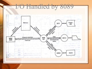
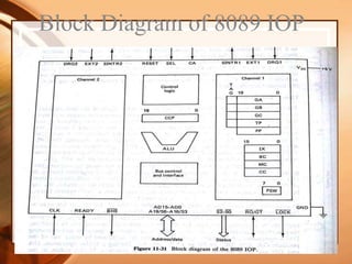
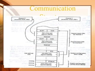
![ Two Channels can be operated
independently.
Sharing common control logic and
ALU.
CCP(Channel Control Pointer)
Cannot be manipulated by the
user
Stores the Control Block
address of channel 1 (during
initialization)
For channel 2 CB
address=[CCP+8]
IOP Architecture](https://image.slidesharecdn.com/14004405-230303024548-aadd3c84/85/8086-Programing-ppt-183-320.jpg)