EC501 MICROPROCESSOR AND
ITS APPLICATIONS
Prof. Ashish Verma
Asst. Professor
Electronics & Communication Department
Mahakal Institute of Technology
Reference and text Books
Advance microprocessor and peripheral –A.K. Ray
and K. M. Bhurchandi, Tata Mcgraw Hill
Microprocessor and Interfacing – D.V.Hall,
McGraw Hill.
• Microprocessor and microcontroller- U. S Shah
• Microprocessor, microcontroller and Embedded
system.
The 8051 microcontroller and embedded
systems-M.A. Mazidi, Janice Gillispie Mazidi,
Pearson Prentice Hall
8/28/2020 Prof.ASHISH VERMA MIT ECE DEPT. 2
Unit 1
• Salient features of advanced microprocessors.
RISC & CISC processors.
• Review and evolution of advanced micro proc
:8086,8088, 80186/286/386/486/Pentium
• Introduction to 8086 processor: Register
organization of 8086,
• Architecture, signal description of 8086,minimum
mode 8086 systems and timings and maximum
mode 8086 systems and timings
8/28/2020 Prof.ASHISH VERMA MIT ECE DEPT. 3
Introduction
• A microprocessor is an
integrated circuit (IC) which
contain all functions of a
computer's central processing
unit (CPU).
• A microprocessor is a
multipurpose,
programmable, clock-driven,
register-based electronic
device that reads binary
instructions from a storage
device called memory and
input output.
8/28/2020 Prof.ASHISH VERMA MIT ECE DEPT. 4
Question in mind?
• Why this IC name is microprocessor?
Ans :This device comprises of transistors which are
small in size (micro-meter).
• What is difference between microprocessor and
microcontroller?
Ans: Although there is a lot of difference between
them but the basic difference is there is no RAM, ROM,
input-output units, timers and other peripherals on the
chip in the microprocessor all are externally interfaced,
but the microcontroller has all these things on chip.
8/28/2020 Prof.ASHISH VERMA MIT ECE DEPT. 5
Types of computer
8/28/2020 Prof.ASHISH VERMA MIT ECE DEPT. 6
Structure of microprocessor
8/28/2020 Prof.ASHISH VERMA MIT ECE DEPT. 7
Evolution of microprocessor
• First microprocessor was invented by
INTEL(INTegrated ELectronics).
Size of microprocessor – 4 bit
Name
Year of
Invention
Clock speed
Number of
transistors
Inst. per sec
INTEL
4004/4040
1971 by Ted
Hoff and
Stanley
Mazor
740 KHz 2300 60,000
8/28/2020 Prof.ASHISH VERMA MIT ECE DEPT. 8
Name
Year of
Invention
Clock speed
Number of
transistors
Inst. per sec
8008 1972 500 KHz 3500 50,000
8080 1974 2 MHz 60,000
10 times faster
than 8008
8085
1976 (16 bit
address bus)
3 MHz 6500 769230
Size of microprocessor – 8 bit
8/28/2020 Prof.ASHISH VERMA MIT ECE DEPT. 9
Size of microprocessor – 16 bit
Name Year of Invention
Clock
speed
Numbe
r of
transist
ors
Inst. per sec
8086
1978 (multiply and divide
instruction, 16 bit data bus
and 20 bit address bus)
4.77
MHz, 8
MHz, 10
MHz
29000 2.5 Million
8088
1979 (cheaper version of
8086 and 8 bit external bus)
2.5 Million
80186/801
88
1982 (80188 cheaper
version of 80186, and
addtional components like
interuppt controller, clock
generator, local bus
controller,counters)
6 MHz
80286
1982 (data bus 16bit and
address bus 24 bit)
8 MHz 134000 4 Million
8/28/2020 Prof.ASHISH VERMA MIT ECE DEPT. 10
Name Year of Invention Clock speed
Number of
transistors
Inst. per sec
INTEL
80386
1986 (other versions
80386DX, 80386SX,
80386SL and data bus
32 bit address bus 32
bit)
16 MHz – 33
MHz
275000
INTEL
80486
1986 (other versions
80486DX, 80486SX,
80486DX2, 80486DX4)
16 MHz –
100 MHz
1.2 Million
transistors
8 KB of cache
memory
PENTIUM 1993 66 MHz
Cache memory
8 bit for
instructions 8
bit for data
8/28/2020 Prof.ASHISH VERMA MIT ECE DEPT. 11
Salient features of advanced microprocessors
• Single +5V power supply
• Clock speed range of 5-10MHz
• capable of executing about 0.33 MIPS (Millions
instructions per second)
• It is 16-bit processor having 16-bit ALU, 16-bit registers,
internal data bus, and 16-bit external data bus resulting
in faster processing.
• It uses two stages of pipelining(begins executing a
second instruction before the first has been
completed), i.e. Fetch Stage and Execute Stage, which
improves performance.
• Fetch stage can prefetch up to 6 bytes of instructions
and stores them in the queue.
• It has 256 interrupts.
8/28/2020 Prof.ASHISH VERMA MIT ECE DEPT. 12
RISC Processor
• It is known as Reduced Instruction Set
Computer. It is a type of microprocessor that
has a limited number of instructions. They can
execute their instructions very fast because
instructions are very small and simple.
• RISC chips require fewer transistors which
make them cheaper to design and produce.
8/28/2020 Prof.ASHISH VERMA MIT ECE DEPT. 13
Characteristic of RISC –
• Simpler instruction, hence simple instruction
decoding.
• Instruction come under size of one word.
• Instruction take single clock cycle to get executed.
• More number of general purpose register.
• Simple Addressing Modes.
• Less Data types.
• Pipeling can be achieved.
8/28/2020 Prof.ASHISH VERMA MIT ECE DEPT. 14
CISC Processor
• The term CISC stands for ‘’Complex Instruction
Set Computer’’. It is a CPU design plan based
on single commands, which are skilled in
executing multi-step operations.
• CISC computers have small programs. It has a
huge number of compound instructions,
which takes a long time to perform
8/28/2020 Prof.ASHISH VERMA MIT ECE DEPT. 15
Characteristic of CISC –
• Complex instruction, hence complex instruction
decoding.
• Instruction are larger than one word size.
• Instruction may take more than single clock cycle
to get executed.
• Less number of general purpose register as
operation get performed in memory itself.
• Complex Addressing Modes.
• More Data types.
8/28/2020 Prof.ASHISH VERMA MIT ECE DEPT. 16
Difference between RISC and CISC
Architecture
8/28/2020 Prof.ASHISH VERMA MIT ECE DEPT. 17
Difference Between CISC and RISC
Architectural
Characterstics
Complex Instruction Set
Computer(CISC)
Reduced Instruction Set
Computer(RISC)
Instruction size and
format
Large set of instructions with
variable formats (16-64 bits per
instruction).
Small set of instructions
with fixed format (32 bit).
Data transfer Memory to memory. Register to register.
CPU control
Most micro coded using control
memory (ROM) but modern
CISC use hardwired control.
Mostly hardwired without
control memory.
Instruction type Not register based instructions. Register based instructions.
Memory access More memory access. Less memory access.
Clocks Includes multi-clocks. Includes single clock.
Instruction nature Instructions are complex.
Instructions are reduced
and simple.
8/28/2020 Prof.ASHISH VERMA MIT ECE DEPT. 18
8086 and 8088 and above
• 8086 (16-bit) & 8088 (8-bit)
• 20-bit addresses
• Two processors which consisted of: Bus
Interface Unit and Execution Unit
• Segmented Memory.
• 80286
Two modes
• 8086 Real Address Mode
• Protected Virtual Address Mode
8/28/2020 Prof.ASHISH VERMA MIT ECE DEPT. 19
Attributes 4004 8008 8080 8086 80286
Date 1971 1972 1974 1978 1982
Transistors 2,300 3,300 4,500 29,000 134,000
Word Size 4-bit 8-bit 8-bit 16-bit 16-bit
Address Size 12-bit 14-bit 16-bit 20-bit 24-bit
Addressable
Memory
4 KB 16 KB 64 KB 1 MB 16 MB
Instructions 46 48 72 133 133+
Max
Frequency
740.74 KHz 800 KHz 2 MHz 10 MHz 12 MHz
8/28/2020 Prof.ASHISH VERMA MIT ECE DEPT. 20
80286 vs. 80386
Attributes 80286 80386
Date 1982 1986
Transistors 134,000 275,000
Word Size 16-bit 32-bit
Address Size 24-bit 32-bit
Addressable Memory 16 MB 4 GB
Max Frequency 12 MHz 33 MHz
Virtual Memory 1 GB 4 GB
8/28/2020 Prof.ASHISH VERMA MIT ECE DEPT. 21
Introduction to 80486
• Increased speed (2 x 80386)
• 80386 with an internal math coprocessor
• Upgradeable (Compatibility)
• Utilize new technology (RISC, cache)
• Segmentation and Paging
• Real Mode vs. Protected Mode
8/28/2020 Prof.ASHISH VERMA MIT ECE DEPT. 22
Intel Pentium
• Released in 1993
• 60/66 MHz Bus Speed
• Two Instruction Pipeline
• Floating Point Calculation
• Floating Point Bug
8/28/2020 Prof.ASHISH VERMA MIT ECE DEPT. 23
8086 Microprocessor
• It is a 16 bit µp.
• Powerful instruction set.
• Capable of multiplication and division
operation.
• 8086 has a 20 bit address bus can access upto
220 memory locations ( 1 MB) .
• 8086 is designed to operate in two modes,
Minimum and Maximum.
8/28/2020 Prof.ASHISH VERMA MIT ECE DEPT. 24
Contd..
• Instruction queue (6 bytes) capability.
• It can support upto 64K I/O ports.
• It provides 16-bit registers.
• It has multiplexed address and data bus AD 0-
AD15 and A16 – A19
• 16 bit address line for I/O
8/28/2020 Prof.ASHISH VERMA MIT ECE DEPT. 25
Register organization of 8086
• 8086 has powerful set of registers
General purpose
 Special purpose
• General purpose can use 8 bit or 16bit.
– Used for hold data and result temporary.
– Store the offset address or counter.
• Special purpose register,
– Segment registers
– Pointer and index registers.
8/28/2020 Prof.ASHISH VERMA MIT ECE DEPT. 26
Categorized in four group
• General data registers.
• Segment registers.
• Pointer and index registers.
• Flag register.
8/28/2020 Prof.ASHISH VERMA MIT ECE DEPT. 27
General data registers
• General purpose registers are used to store
temporary data within the microprocessor.
• The four general purpose registers are the AX, BX,
CX, and DX registers.
AX - accumulator, and preferred for most operations.
BX - base register, typically used to hold the address of
a procedure or variable.
CX - count register, typically used for looping.
DX - data register, typically used for multiplication and
division.
8/28/2020 Prof.ASHISH VERMA MIT ECE DEPT. 28
Contd…
• All of the general purpose registers can be
treated as a 16 bit quantity or as two 8 bit
quantities. The high byte is referenced by
replacing the X with H. The low byte is
referenced by replacing the X with L:
8/28/2020 Prof.ASHISH VERMA MIT ECE DEPT. 29
Segment Registers
• Four Segment registers. All are 16 bit registers.
CS - points at the segment containing the current
program. Addressing CS memory
DS - generally points at segment where variables
are defined.
ES - extra segment register, it's up to a coder to
define its usage.
SS - points at the segment containing the stack.
8/28/2020 Prof.ASHISH VERMA MIT ECE DEPT. 30
Contd..
• 8086 address 1M byte segmented memory
which is divided into 16 logical segment.
• Each segment Contains 64k bytes of memory.
• 1 MB= 1048576 and 2^16= 65536.
• Segment register hold the upper 16 bits of
starting address of four memory segment.
• 20 bits add.of RAM = Segment reg. add + 4bit
8/28/2020 Prof.ASHISH VERMA MIT ECE DEPT. 31
Physical address calculation format
• Physical address(RAM location address 20 bit)
= Segment address + offset
(16bit)+(4 Zero)+ offset address.
• Example:
Data segment :2000H
Source index(offset): 1F23
Append hard wired zero: 0000
Phy add= 2000
0000
20000 (20bit) + 1F23(16bit)= 21F23
8/28/2020 Prof.ASHISH VERMA MIT ECE DEPT. 32
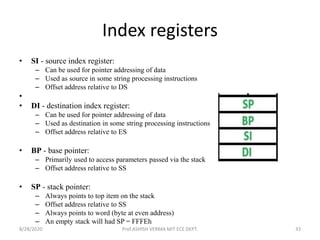
Index registers
• SI - source index register:
– Can be used for pointer addressing of data
– Used as source in some string processing instructions
– Offset address relative to DS
•
• DI - destination index register:
– Can be used for pointer addressing of data
– Used as destination in some string processing instructions
– Offset address relative to ES
• BP - base pointer:
– Primarily used to access parameters passed via the stack
– Offset address relative to SS
• SP - stack pointer:
– Always points to top item on the stack
– Offset address relative to SS
– Always points to word (byte at even address)
– An empty stack will had SP = FFFEh
8/28/2020 Prof.ASHISH VERMA MIT ECE DEPT. 33
– The pointer register IP contains offset within the code
segment.
– The pointer register BP contains offset within the data
segment.
– He pointer register SP contains offset within the stack
segment.
– The register SI is used to store the offset of source
data in data segment.
– The register DI is used to store the offset of
destination in data or extra segment.
8/28/2020 Prof.ASHISH VERMA MIT ECE DEPT. 34
Flag register
• Flags Register - determines the current state of
the processor.
• Flags Register is modified automatically by CPU
after mathematical operations. This allows to
determine the type of the result.
• Generally you cannot access these registers
directly.
• The FLAGS register is the status
register in Intel x86 microprocessors that contains
the current state of the processor.
8/28/2020 Prof.ASHISH VERMA MIT ECE DEPT. 35
• There are total 9 flags in 8086 and the flag register is divided
into two types:
• (a) Status Flags – S,Z,AC,CF,PF,O
• (b)Control Flag – DF,IF,TF
8/28/2020 Prof.ASHISH VERMA MIT ECE DEPT. 36
• Carry Flag (CF) - this flag is set to 1 when there is
an unsigned overflow. For example when you add
bytes 255 + 1 (result is not in range 0...255). When
there is no overflow this flag is set to 0.
• Parity Flag (PF) - this flag is set to 1 when there is
even number of one bits in result, and to 0 when there
is odd number of one bits. Even if result is a word
only 8 low bits are analyzed!
• Auxiliary Flag (AF) - set to 1 when there is
an unsigned overflow for low nibble (4 bits).
• Zero Flag (ZF) - set to 1 when result is zero. For
none zero result this flag is set to 0.
8/28/2020 Prof.ASHISH VERMA MIT ECE DEPT. 37
• Sign Flag (SF) - set to 1 when result is negative. When result
is positive it is set to 0. Actually this flag take the value of the
most significant bit.
• Trap Flag (TF) - Used for on-chip debugging. An interrupt,
also known as a trap, can occur whenever an invalid operation
occurs within a processor, be it an illegal memory access, wrong
opcode, division by zero, overflow etc.
• Interrupt enable Flag (IF) - when this flag is set to 1 CPU
reacts to interrupts from external devices.
• Direction Flag (DF) - this flag is used by some instructions to
process data chains, when this flag is set to 0 - the processing is
done forward, when this flag is set to 1 the processing is done
backward.
• Overflow Flag (OF) - set to 1 when there is a signed overflow.
For example, when you add bytes 100 + 50 (result is not in
range -128...127).
8/28/2020 Prof.ASHISH VERMA MIT ECE DEPT. 38
Architecture of 8086
• The Bus Interface Unit(BIU): It provides the
interface of 8086 to external memory and I/O
devices via the System Bus.
• The Execution Unit (EU): Execution unit gives
instructions to BIU stating from where to fetch
the data and then decode and execute those
instructions.
8/28/2020 Prof.ASHISH VERMA MIT ECE DEPT. 39
8/28/2020 Prof.ASHISH VERMA MIT ECE DEPT. 40
BIU performs the following functions-
• It generates the 20 bit physical address for
memory access.
• It fetches instructions from the memory.
• It transfers data to and from the memory and I/O.
• Maintains the 6 byte pre fetch instruction
queue(supports pipelining).
• Instruction Pointer (IP): It is a 16 bit register. It
holds offset of the next instructions in the Code
Segment.
8/28/2020 Prof.ASHISH VERMA MIT ECE DEPT. 41
• Code segment Register CS holds the segment
address which is 4569 H
Instruction pointer IP holds the offset address
which is 10A0 H
The physical 20-bit address is calculated as
follows.
• Segment address : 45690 H
Offset address :+ 10A0 H
Physical address : 46730 H
8/28/2020 Prof.ASHISH VERMA MIT ECE DEPT. 42
EU performs the following functions-
• Fetches instructions from the Queue in BIU,
decodes and executes arithmetic and logic
operations using the ALU.
• Sends control signals for internal data transfer
operations within the microprocessor.
• Sends request signals to the BIU to access the
external module.
• It operates with respect to T-states (clock
cycles) and not machine cycles.
8/28/2020 Prof.ASHISH VERMA MIT ECE DEPT. 43
8086 pin diagram
• 8086 was the first 16-bit microprocessor available
in 40-pin DIP (Dual Inline Package) chip.
• Dual in-line pin package is an electronic
component package with a rectangular housing
and two parallel rows of electrical connecting
pins.
• Intel 8086 is a 16-bit HMOS microprocessor.
• The 16-low order address bus lines have been
multiplexed with data and 4 high-order address
bus lines have been multiplexed with status
signals.
8/28/2020 Prof.ASHISH VERMA MIT ECE DEPT. 44
8/28/2020 Prof.ASHISH VERMA MIT ECE DEPT. 45
• Power supply: It uses 5V DC supply at VCC pin 40, and uses
ground at VSS pin 1 and 20 for its operation.
• Clock signal: Clock signal is provided through Pin-19. It
provides timing to the processor for operations. Its frequency
is different for different versions, i.e. 5MHz, 8MHz and
10MHz.
• AD0-AD15 : Address/Data bus. These are low order address
bus. They are multiplexed with data. AD0-AD7 carries low
order byte data and AD8-AD15 carries higher order byte
data. During the first clock cycle, it carries 16-bit address and
after that it carries 16-bit data.
• Address/status bus: A16-A19/S3-S6 These are the 4
address/status buses. During the first clock cycle, it carries 4-
bit address and later it carries status signals.
8/28/2020 Prof.ASHISH VERMA MIT ECE DEPT. 46
• S2, S1, S0 Status pins:
S2 S1 S0 CHARACTERISTICS
0 0 0
Interrupt
acknowledge
0 0 1 Read I/O port
0 1 0 Write I/O port
0 1 1 Halt
1 0 0 Code access
1 0 1 Read memory
1 1 0 Write memory
1 1 1 Passive state
8/28/2020 Prof.ASHISH VERMA MIT ECE DEPT. 47
• A16/S3, A17/S4, A18/S5, A19/S6 : The
specified address lines are multiplexed with
corresponding status signals.
A17/S4 A16/S3 FUNCTION
0 0 Extra segment access
0 1 Stack segment access
1 0 Code segment access
1 1 Data segment access
8/28/2020 Prof.ASHISH VERMA MIT ECE DEPT. 48
• BHE’/S7 : Bus High Enable/Status. During T1 it is
low. It is used to enable data onto the most significant
half of data bus, D8-D15. 8-bit device connected to
upper half of the data bus use BHE (Active Low)
signal. It is multiplexed with status signal S7. S7 signal
is available during T2, T3 & T4.
• RD’: It is available at pin 32 and is used to read signal
for Read operation. It is an output signal. Active low.
• READY : This is the acknowledgement from the
memory or slow device that they have completed the
data transfer. It is an active high signal. When it is high,
it indicates that the device is ready to transfer data.
When it is low, it indicates wait state.
8/28/2020 Prof.ASHISH VERMA MIT ECE DEPT. 49
• RESET: It is available at pin 21 and is used to
restart the execution. It causes the processor to
immediately terminate its present activity. This
signal is active high for the first 4 clock cycles to
RESET the microprocessor.
• INTER: It is available at pin 18. It is an interrupt
request signal, which is sampled during the last
clock cycle of each instruction to determine if the
processor considered this as an interrupt or not.
• NMI: It stands for non-maskable interrupt and is
available at pin 17. It is an edge triggered input,
which causes an interrupt request to the
microprocessor.
8/28/2020 Prof.ASHISH VERMA MIT ECE DEPT. 50
• TEST: This signal is like wait state and is available
at pin 23. When this signal is high, then the
processor has to wait for IDLE state, else the
execution continues.
• MN/MX’: It stands for Minimum/Maximum and
is available at pin 33. It indicates what mode the
processor is to operate in; when it is high, it
works in the minimum mode and vice-versa.
• INTA: It is an interrupt acknowledgement signal
and is available at pin 24. When the
microprocessor receives this signal, it
acknowledges the interrupt.
8/28/2020 Prof.ASHISH VERMA MIT ECE DEPT. 51
ALE
• It stands for address enable latch and is available at pin 25. A
positive pulse is generated each time the processor begins
any operation. This signal indicates the availability of a valid
address on the address/data lines.
8/28/2020 Prof.ASHISH VERMA MIT ECE DEPT. 52
• DEN: It stands for Data Enable and is available at
pin 26. It is used to enable Transreceiver 8286.
The transreceiver is a device used to separate
data from the address/data bus.
• DT/R: It stands for Data Transmit/Receive signal
and is available at pin 27. It decides the direction
of data flow through the transreceiver. When it is
high, data is transmitted out and vice-a-versa.
• IO/M’: This signal is used to distinguish between
memory and I/O operations. When it is high, it
indicates I/O operation and when it is low
indicates the memory operation. It is available at
pin 28.
8/28/2020 Prof.ASHISH VERMA MIT ECE DEPT. 53
• WR: It stands for write signal and is available at pin 29.
It is used to write the data into the memory or the
output device depending on the status of M/IO signal.
• HLDA: It stands for Hold Acknowledgement signal and
is available at pin 30. This signal acknowledges the
HOLD signal.
• HOLD: This signal indicates to the processor that
external devices are requesting to access the
address/data buses. It is available at pin 31.
• LOCK: Its an active low pin. It indicates that other
system bus masters have not been allowed to gain
control of the system bus while LOCK’ is active low(0).
The LOCK signal will be active until the completion of
the next instruction and is available at pin 29.
8/28/2020 Prof.ASHISH VERMA MIT ECE DEPT. 54
• RQ/GT1 and RQ/GT0: These are the Request/Grant
signals used by the other processors requesting the CPU
to release the system bus. When the signal is received by
CPU, then it sends acknowledgment. RQ/GT0 has a
higher priority than RQ/GT1.
• QS1 and QS0: These are queue status signals and are
available at pin 24 and 25. These signals provide the
status of instruction queue. Their conditions are shown
in the following table −
QS0 QS1 Status
0 0 No operation
0 1 First byte of opcode from the queue
1 0 Empty the queue
1 1 Subsequent byte from the queue
8/28/2020 Prof.ASHISH VERMA MIT ECE DEPT. 55
Minimum mode 8086
8/28/2020 Prof.ASHISH VERMA MIT ECE DEPT. 56
8/28/2020 Prof.ASHISH VERMA MIT ECE DEPT. 57
8/28/2020 Prof.ASHISH VERMA MIT ECE DEPT. 58
Maximum mode 8086
8/28/2020 Prof.ASHISH VERMA MIT ECE DEPT. 59
8/28/2020 Prof.ASHISH VERMA MIT ECE DEPT. 60
8/28/2020 Prof.ASHISH VERMA MIT ECE DEPT. 61
8/28/2020 Prof.ASHISH VERMA MIT ECE DEPT. 62
8/28/2020 Prof.ASHISH VERMA MIT ECE DEPT. 63
8/28/2020 Prof.ASHISH VERMA MIT ECE DEPT. 64
• Machine Cycle:
– It is the time required to complete one operation of accessing
memory/ I/o, either Memory write, Memory Read, I/o read or
I/O write
– The time required by the microprocessor to complete an
operation of accessing memory or input/output devices is
called machine cycle.
• T state:
– It is defined as the one subdivision of operation performed in one
clock period.
– One time period of frequency of microprocessor is called t-state.
– A t-state is measured from the falling edge of one clock pulse to
the falling edge of the next clock pulse. Fetch cycle takes four t-
states and execution cycle takes three t-states.
• Instruction Cycle:
– The Steps required by CPU to fetch and execute an Instruction is
called a Instruction Cycle. It consist of fetch and Execute Cycle.
8/28/2020 Prof.ASHISH VERMA MIT ECE DEPT. 65
8/28/2020 Prof.ASHISH VERMA MIT ECE DEPT. 66
8/28/2020 Prof.ASHISH VERMA MIT ECE DEPT. 67

Microprocessor 8086 Cover Unit I

  • 1.
    EC501 MICROPROCESSOR AND ITSAPPLICATIONS Prof. Ashish Verma Asst. Professor Electronics & Communication Department Mahakal Institute of Technology
  • 2.
    Reference and textBooks Advance microprocessor and peripheral –A.K. Ray and K. M. Bhurchandi, Tata Mcgraw Hill Microprocessor and Interfacing – D.V.Hall, McGraw Hill. • Microprocessor and microcontroller- U. S Shah • Microprocessor, microcontroller and Embedded system. The 8051 microcontroller and embedded systems-M.A. Mazidi, Janice Gillispie Mazidi, Pearson Prentice Hall 8/28/2020 Prof.ASHISH VERMA MIT ECE DEPT. 2
  • 3.
    Unit 1 • Salientfeatures of advanced microprocessors. RISC & CISC processors. • Review and evolution of advanced micro proc :8086,8088, 80186/286/386/486/Pentium • Introduction to 8086 processor: Register organization of 8086, • Architecture, signal description of 8086,minimum mode 8086 systems and timings and maximum mode 8086 systems and timings 8/28/2020 Prof.ASHISH VERMA MIT ECE DEPT. 3
  • 4.
    Introduction • A microprocessoris an integrated circuit (IC) which contain all functions of a computer's central processing unit (CPU). • A microprocessor is a multipurpose, programmable, clock-driven, register-based electronic device that reads binary instructions from a storage device called memory and input output. 8/28/2020 Prof.ASHISH VERMA MIT ECE DEPT. 4
  • 5.
    Question in mind? •Why this IC name is microprocessor? Ans :This device comprises of transistors which are small in size (micro-meter). • What is difference between microprocessor and microcontroller? Ans: Although there is a lot of difference between them but the basic difference is there is no RAM, ROM, input-output units, timers and other peripherals on the chip in the microprocessor all are externally interfaced, but the microcontroller has all these things on chip. 8/28/2020 Prof.ASHISH VERMA MIT ECE DEPT. 5
  • 6.
    Types of computer 8/28/2020Prof.ASHISH VERMA MIT ECE DEPT. 6
  • 7.
    Structure of microprocessor 8/28/2020Prof.ASHISH VERMA MIT ECE DEPT. 7
  • 8.
    Evolution of microprocessor •First microprocessor was invented by INTEL(INTegrated ELectronics). Size of microprocessor – 4 bit Name Year of Invention Clock speed Number of transistors Inst. per sec INTEL 4004/4040 1971 by Ted Hoff and Stanley Mazor 740 KHz 2300 60,000 8/28/2020 Prof.ASHISH VERMA MIT ECE DEPT. 8
  • 9.
    Name Year of Invention Clock speed Numberof transistors Inst. per sec 8008 1972 500 KHz 3500 50,000 8080 1974 2 MHz 60,000 10 times faster than 8008 8085 1976 (16 bit address bus) 3 MHz 6500 769230 Size of microprocessor – 8 bit 8/28/2020 Prof.ASHISH VERMA MIT ECE DEPT. 9
  • 10.
    Size of microprocessor– 16 bit Name Year of Invention Clock speed Numbe r of transist ors Inst. per sec 8086 1978 (multiply and divide instruction, 16 bit data bus and 20 bit address bus) 4.77 MHz, 8 MHz, 10 MHz 29000 2.5 Million 8088 1979 (cheaper version of 8086 and 8 bit external bus) 2.5 Million 80186/801 88 1982 (80188 cheaper version of 80186, and addtional components like interuppt controller, clock generator, local bus controller,counters) 6 MHz 80286 1982 (data bus 16bit and address bus 24 bit) 8 MHz 134000 4 Million 8/28/2020 Prof.ASHISH VERMA MIT ECE DEPT. 10
  • 11.
    Name Year ofInvention Clock speed Number of transistors Inst. per sec INTEL 80386 1986 (other versions 80386DX, 80386SX, 80386SL and data bus 32 bit address bus 32 bit) 16 MHz – 33 MHz 275000 INTEL 80486 1986 (other versions 80486DX, 80486SX, 80486DX2, 80486DX4) 16 MHz – 100 MHz 1.2 Million transistors 8 KB of cache memory PENTIUM 1993 66 MHz Cache memory 8 bit for instructions 8 bit for data 8/28/2020 Prof.ASHISH VERMA MIT ECE DEPT. 11
  • 12.
    Salient features ofadvanced microprocessors • Single +5V power supply • Clock speed range of 5-10MHz • capable of executing about 0.33 MIPS (Millions instructions per second) • It is 16-bit processor having 16-bit ALU, 16-bit registers, internal data bus, and 16-bit external data bus resulting in faster processing. • It uses two stages of pipelining(begins executing a second instruction before the first has been completed), i.e. Fetch Stage and Execute Stage, which improves performance. • Fetch stage can prefetch up to 6 bytes of instructions and stores them in the queue. • It has 256 interrupts. 8/28/2020 Prof.ASHISH VERMA MIT ECE DEPT. 12
  • 13.
    RISC Processor • Itis known as Reduced Instruction Set Computer. It is a type of microprocessor that has a limited number of instructions. They can execute their instructions very fast because instructions are very small and simple. • RISC chips require fewer transistors which make them cheaper to design and produce. 8/28/2020 Prof.ASHISH VERMA MIT ECE DEPT. 13
  • 14.
    Characteristic of RISC– • Simpler instruction, hence simple instruction decoding. • Instruction come under size of one word. • Instruction take single clock cycle to get executed. • More number of general purpose register. • Simple Addressing Modes. • Less Data types. • Pipeling can be achieved. 8/28/2020 Prof.ASHISH VERMA MIT ECE DEPT. 14
  • 15.
    CISC Processor • Theterm CISC stands for ‘’Complex Instruction Set Computer’’. It is a CPU design plan based on single commands, which are skilled in executing multi-step operations. • CISC computers have small programs. It has a huge number of compound instructions, which takes a long time to perform 8/28/2020 Prof.ASHISH VERMA MIT ECE DEPT. 15
  • 16.
    Characteristic of CISC– • Complex instruction, hence complex instruction decoding. • Instruction are larger than one word size. • Instruction may take more than single clock cycle to get executed. • Less number of general purpose register as operation get performed in memory itself. • Complex Addressing Modes. • More Data types. 8/28/2020 Prof.ASHISH VERMA MIT ECE DEPT. 16
  • 17.
    Difference between RISCand CISC Architecture 8/28/2020 Prof.ASHISH VERMA MIT ECE DEPT. 17
  • 18.
    Difference Between CISCand RISC Architectural Characterstics Complex Instruction Set Computer(CISC) Reduced Instruction Set Computer(RISC) Instruction size and format Large set of instructions with variable formats (16-64 bits per instruction). Small set of instructions with fixed format (32 bit). Data transfer Memory to memory. Register to register. CPU control Most micro coded using control memory (ROM) but modern CISC use hardwired control. Mostly hardwired without control memory. Instruction type Not register based instructions. Register based instructions. Memory access More memory access. Less memory access. Clocks Includes multi-clocks. Includes single clock. Instruction nature Instructions are complex. Instructions are reduced and simple. 8/28/2020 Prof.ASHISH VERMA MIT ECE DEPT. 18
  • 19.
    8086 and 8088and above • 8086 (16-bit) & 8088 (8-bit) • 20-bit addresses • Two processors which consisted of: Bus Interface Unit and Execution Unit • Segmented Memory. • 80286 Two modes • 8086 Real Address Mode • Protected Virtual Address Mode 8/28/2020 Prof.ASHISH VERMA MIT ECE DEPT. 19
  • 20.
    Attributes 4004 80088080 8086 80286 Date 1971 1972 1974 1978 1982 Transistors 2,300 3,300 4,500 29,000 134,000 Word Size 4-bit 8-bit 8-bit 16-bit 16-bit Address Size 12-bit 14-bit 16-bit 20-bit 24-bit Addressable Memory 4 KB 16 KB 64 KB 1 MB 16 MB Instructions 46 48 72 133 133+ Max Frequency 740.74 KHz 800 KHz 2 MHz 10 MHz 12 MHz 8/28/2020 Prof.ASHISH VERMA MIT ECE DEPT. 20
  • 21.
    80286 vs. 80386 Attributes80286 80386 Date 1982 1986 Transistors 134,000 275,000 Word Size 16-bit 32-bit Address Size 24-bit 32-bit Addressable Memory 16 MB 4 GB Max Frequency 12 MHz 33 MHz Virtual Memory 1 GB 4 GB 8/28/2020 Prof.ASHISH VERMA MIT ECE DEPT. 21
  • 22.
    Introduction to 80486 •Increased speed (2 x 80386) • 80386 with an internal math coprocessor • Upgradeable (Compatibility) • Utilize new technology (RISC, cache) • Segmentation and Paging • Real Mode vs. Protected Mode 8/28/2020 Prof.ASHISH VERMA MIT ECE DEPT. 22
  • 23.
    Intel Pentium • Releasedin 1993 • 60/66 MHz Bus Speed • Two Instruction Pipeline • Floating Point Calculation • Floating Point Bug 8/28/2020 Prof.ASHISH VERMA MIT ECE DEPT. 23
  • 24.
    8086 Microprocessor • Itis a 16 bit µp. • Powerful instruction set. • Capable of multiplication and division operation. • 8086 has a 20 bit address bus can access upto 220 memory locations ( 1 MB) . • 8086 is designed to operate in two modes, Minimum and Maximum. 8/28/2020 Prof.ASHISH VERMA MIT ECE DEPT. 24
  • 25.
    Contd.. • Instruction queue(6 bytes) capability. • It can support upto 64K I/O ports. • It provides 16-bit registers. • It has multiplexed address and data bus AD 0- AD15 and A16 – A19 • 16 bit address line for I/O 8/28/2020 Prof.ASHISH VERMA MIT ECE DEPT. 25
  • 26.
    Register organization of8086 • 8086 has powerful set of registers General purpose  Special purpose • General purpose can use 8 bit or 16bit. – Used for hold data and result temporary. – Store the offset address or counter. • Special purpose register, – Segment registers – Pointer and index registers. 8/28/2020 Prof.ASHISH VERMA MIT ECE DEPT. 26
  • 27.
    Categorized in fourgroup • General data registers. • Segment registers. • Pointer and index registers. • Flag register. 8/28/2020 Prof.ASHISH VERMA MIT ECE DEPT. 27
  • 28.
    General data registers •General purpose registers are used to store temporary data within the microprocessor. • The four general purpose registers are the AX, BX, CX, and DX registers. AX - accumulator, and preferred for most operations. BX - base register, typically used to hold the address of a procedure or variable. CX - count register, typically used for looping. DX - data register, typically used for multiplication and division. 8/28/2020 Prof.ASHISH VERMA MIT ECE DEPT. 28
  • 29.
    Contd… • All ofthe general purpose registers can be treated as a 16 bit quantity or as two 8 bit quantities. The high byte is referenced by replacing the X with H. The low byte is referenced by replacing the X with L: 8/28/2020 Prof.ASHISH VERMA MIT ECE DEPT. 29
  • 30.
    Segment Registers • FourSegment registers. All are 16 bit registers. CS - points at the segment containing the current program. Addressing CS memory DS - generally points at segment where variables are defined. ES - extra segment register, it's up to a coder to define its usage. SS - points at the segment containing the stack. 8/28/2020 Prof.ASHISH VERMA MIT ECE DEPT. 30
  • 31.
    Contd.. • 8086 address1M byte segmented memory which is divided into 16 logical segment. • Each segment Contains 64k bytes of memory. • 1 MB= 1048576 and 2^16= 65536. • Segment register hold the upper 16 bits of starting address of four memory segment. • 20 bits add.of RAM = Segment reg. add + 4bit 8/28/2020 Prof.ASHISH VERMA MIT ECE DEPT. 31
  • 32.
    Physical address calculationformat • Physical address(RAM location address 20 bit) = Segment address + offset (16bit)+(4 Zero)+ offset address. • Example: Data segment :2000H Source index(offset): 1F23 Append hard wired zero: 0000 Phy add= 2000 0000 20000 (20bit) + 1F23(16bit)= 21F23 8/28/2020 Prof.ASHISH VERMA MIT ECE DEPT. 32
  • 33.
    Index registers • SI- source index register: – Can be used for pointer addressing of data – Used as source in some string processing instructions – Offset address relative to DS • • DI - destination index register: – Can be used for pointer addressing of data – Used as destination in some string processing instructions – Offset address relative to ES • BP - base pointer: – Primarily used to access parameters passed via the stack – Offset address relative to SS • SP - stack pointer: – Always points to top item on the stack – Offset address relative to SS – Always points to word (byte at even address) – An empty stack will had SP = FFFEh 8/28/2020 Prof.ASHISH VERMA MIT ECE DEPT. 33
  • 34.
    – The pointerregister IP contains offset within the code segment. – The pointer register BP contains offset within the data segment. – He pointer register SP contains offset within the stack segment. – The register SI is used to store the offset of source data in data segment. – The register DI is used to store the offset of destination in data or extra segment. 8/28/2020 Prof.ASHISH VERMA MIT ECE DEPT. 34
  • 35.
    Flag register • FlagsRegister - determines the current state of the processor. • Flags Register is modified automatically by CPU after mathematical operations. This allows to determine the type of the result. • Generally you cannot access these registers directly. • The FLAGS register is the status register in Intel x86 microprocessors that contains the current state of the processor. 8/28/2020 Prof.ASHISH VERMA MIT ECE DEPT. 35
  • 36.
    • There aretotal 9 flags in 8086 and the flag register is divided into two types: • (a) Status Flags – S,Z,AC,CF,PF,O • (b)Control Flag – DF,IF,TF 8/28/2020 Prof.ASHISH VERMA MIT ECE DEPT. 36
  • 37.
    • Carry Flag(CF) - this flag is set to 1 when there is an unsigned overflow. For example when you add bytes 255 + 1 (result is not in range 0...255). When there is no overflow this flag is set to 0. • Parity Flag (PF) - this flag is set to 1 when there is even number of one bits in result, and to 0 when there is odd number of one bits. Even if result is a word only 8 low bits are analyzed! • Auxiliary Flag (AF) - set to 1 when there is an unsigned overflow for low nibble (4 bits). • Zero Flag (ZF) - set to 1 when result is zero. For none zero result this flag is set to 0. 8/28/2020 Prof.ASHISH VERMA MIT ECE DEPT. 37
  • 38.
    • Sign Flag(SF) - set to 1 when result is negative. When result is positive it is set to 0. Actually this flag take the value of the most significant bit. • Trap Flag (TF) - Used for on-chip debugging. An interrupt, also known as a trap, can occur whenever an invalid operation occurs within a processor, be it an illegal memory access, wrong opcode, division by zero, overflow etc. • Interrupt enable Flag (IF) - when this flag is set to 1 CPU reacts to interrupts from external devices. • Direction Flag (DF) - this flag is used by some instructions to process data chains, when this flag is set to 0 - the processing is done forward, when this flag is set to 1 the processing is done backward. • Overflow Flag (OF) - set to 1 when there is a signed overflow. For example, when you add bytes 100 + 50 (result is not in range -128...127). 8/28/2020 Prof.ASHISH VERMA MIT ECE DEPT. 38
  • 39.
    Architecture of 8086 •The Bus Interface Unit(BIU): It provides the interface of 8086 to external memory and I/O devices via the System Bus. • The Execution Unit (EU): Execution unit gives instructions to BIU stating from where to fetch the data and then decode and execute those instructions. 8/28/2020 Prof.ASHISH VERMA MIT ECE DEPT. 39
  • 40.
  • 41.
    BIU performs thefollowing functions- • It generates the 20 bit physical address for memory access. • It fetches instructions from the memory. • It transfers data to and from the memory and I/O. • Maintains the 6 byte pre fetch instruction queue(supports pipelining). • Instruction Pointer (IP): It is a 16 bit register. It holds offset of the next instructions in the Code Segment. 8/28/2020 Prof.ASHISH VERMA MIT ECE DEPT. 41
  • 42.
    • Code segmentRegister CS holds the segment address which is 4569 H Instruction pointer IP holds the offset address which is 10A0 H The physical 20-bit address is calculated as follows. • Segment address : 45690 H Offset address :+ 10A0 H Physical address : 46730 H 8/28/2020 Prof.ASHISH VERMA MIT ECE DEPT. 42
  • 43.
    EU performs thefollowing functions- • Fetches instructions from the Queue in BIU, decodes and executes arithmetic and logic operations using the ALU. • Sends control signals for internal data transfer operations within the microprocessor. • Sends request signals to the BIU to access the external module. • It operates with respect to T-states (clock cycles) and not machine cycles. 8/28/2020 Prof.ASHISH VERMA MIT ECE DEPT. 43
  • 44.
    8086 pin diagram •8086 was the first 16-bit microprocessor available in 40-pin DIP (Dual Inline Package) chip. • Dual in-line pin package is an electronic component package with a rectangular housing and two parallel rows of electrical connecting pins. • Intel 8086 is a 16-bit HMOS microprocessor. • The 16-low order address bus lines have been multiplexed with data and 4 high-order address bus lines have been multiplexed with status signals. 8/28/2020 Prof.ASHISH VERMA MIT ECE DEPT. 44
  • 45.
  • 46.
    • Power supply:It uses 5V DC supply at VCC pin 40, and uses ground at VSS pin 1 and 20 for its operation. • Clock signal: Clock signal is provided through Pin-19. It provides timing to the processor for operations. Its frequency is different for different versions, i.e. 5MHz, 8MHz and 10MHz. • AD0-AD15 : Address/Data bus. These are low order address bus. They are multiplexed with data. AD0-AD7 carries low order byte data and AD8-AD15 carries higher order byte data. During the first clock cycle, it carries 16-bit address and after that it carries 16-bit data. • Address/status bus: A16-A19/S3-S6 These are the 4 address/status buses. During the first clock cycle, it carries 4- bit address and later it carries status signals. 8/28/2020 Prof.ASHISH VERMA MIT ECE DEPT. 46
  • 47.
    • S2, S1,S0 Status pins: S2 S1 S0 CHARACTERISTICS 0 0 0 Interrupt acknowledge 0 0 1 Read I/O port 0 1 0 Write I/O port 0 1 1 Halt 1 0 0 Code access 1 0 1 Read memory 1 1 0 Write memory 1 1 1 Passive state 8/28/2020 Prof.ASHISH VERMA MIT ECE DEPT. 47
  • 48.
    • A16/S3, A17/S4,A18/S5, A19/S6 : The specified address lines are multiplexed with corresponding status signals. A17/S4 A16/S3 FUNCTION 0 0 Extra segment access 0 1 Stack segment access 1 0 Code segment access 1 1 Data segment access 8/28/2020 Prof.ASHISH VERMA MIT ECE DEPT. 48
  • 49.
    • BHE’/S7 :Bus High Enable/Status. During T1 it is low. It is used to enable data onto the most significant half of data bus, D8-D15. 8-bit device connected to upper half of the data bus use BHE (Active Low) signal. It is multiplexed with status signal S7. S7 signal is available during T2, T3 & T4. • RD’: It is available at pin 32 and is used to read signal for Read operation. It is an output signal. Active low. • READY : This is the acknowledgement from the memory or slow device that they have completed the data transfer. It is an active high signal. When it is high, it indicates that the device is ready to transfer data. When it is low, it indicates wait state. 8/28/2020 Prof.ASHISH VERMA MIT ECE DEPT. 49
  • 50.
    • RESET: Itis available at pin 21 and is used to restart the execution. It causes the processor to immediately terminate its present activity. This signal is active high for the first 4 clock cycles to RESET the microprocessor. • INTER: It is available at pin 18. It is an interrupt request signal, which is sampled during the last clock cycle of each instruction to determine if the processor considered this as an interrupt or not. • NMI: It stands for non-maskable interrupt and is available at pin 17. It is an edge triggered input, which causes an interrupt request to the microprocessor. 8/28/2020 Prof.ASHISH VERMA MIT ECE DEPT. 50
  • 51.
    • TEST: Thissignal is like wait state and is available at pin 23. When this signal is high, then the processor has to wait for IDLE state, else the execution continues. • MN/MX’: It stands for Minimum/Maximum and is available at pin 33. It indicates what mode the processor is to operate in; when it is high, it works in the minimum mode and vice-versa. • INTA: It is an interrupt acknowledgement signal and is available at pin 24. When the microprocessor receives this signal, it acknowledges the interrupt. 8/28/2020 Prof.ASHISH VERMA MIT ECE DEPT. 51
  • 52.
    ALE • It standsfor address enable latch and is available at pin 25. A positive pulse is generated each time the processor begins any operation. This signal indicates the availability of a valid address on the address/data lines. 8/28/2020 Prof.ASHISH VERMA MIT ECE DEPT. 52
  • 53.
    • DEN: Itstands for Data Enable and is available at pin 26. It is used to enable Transreceiver 8286. The transreceiver is a device used to separate data from the address/data bus. • DT/R: It stands for Data Transmit/Receive signal and is available at pin 27. It decides the direction of data flow through the transreceiver. When it is high, data is transmitted out and vice-a-versa. • IO/M’: This signal is used to distinguish between memory and I/O operations. When it is high, it indicates I/O operation and when it is low indicates the memory operation. It is available at pin 28. 8/28/2020 Prof.ASHISH VERMA MIT ECE DEPT. 53
  • 54.
    • WR: Itstands for write signal and is available at pin 29. It is used to write the data into the memory or the output device depending on the status of M/IO signal. • HLDA: It stands for Hold Acknowledgement signal and is available at pin 30. This signal acknowledges the HOLD signal. • HOLD: This signal indicates to the processor that external devices are requesting to access the address/data buses. It is available at pin 31. • LOCK: Its an active low pin. It indicates that other system bus masters have not been allowed to gain control of the system bus while LOCK’ is active low(0). The LOCK signal will be active until the completion of the next instruction and is available at pin 29. 8/28/2020 Prof.ASHISH VERMA MIT ECE DEPT. 54
  • 55.
    • RQ/GT1 andRQ/GT0: These are the Request/Grant signals used by the other processors requesting the CPU to release the system bus. When the signal is received by CPU, then it sends acknowledgment. RQ/GT0 has a higher priority than RQ/GT1. • QS1 and QS0: These are queue status signals and are available at pin 24 and 25. These signals provide the status of instruction queue. Their conditions are shown in the following table − QS0 QS1 Status 0 0 No operation 0 1 First byte of opcode from the queue 1 0 Empty the queue 1 1 Subsequent byte from the queue 8/28/2020 Prof.ASHISH VERMA MIT ECE DEPT. 55
  • 56.
    Minimum mode 8086 8/28/2020Prof.ASHISH VERMA MIT ECE DEPT. 56
  • 57.
  • 58.
  • 59.
    Maximum mode 8086 8/28/2020Prof.ASHISH VERMA MIT ECE DEPT. 59
  • 60.
  • 61.
  • 62.
  • 63.
  • 64.
  • 65.
    • Machine Cycle: –It is the time required to complete one operation of accessing memory/ I/o, either Memory write, Memory Read, I/o read or I/O write – The time required by the microprocessor to complete an operation of accessing memory or input/output devices is called machine cycle. • T state: – It is defined as the one subdivision of operation performed in one clock period. – One time period of frequency of microprocessor is called t-state. – A t-state is measured from the falling edge of one clock pulse to the falling edge of the next clock pulse. Fetch cycle takes four t- states and execution cycle takes three t-states. • Instruction Cycle: – The Steps required by CPU to fetch and execute an Instruction is called a Instruction Cycle. It consist of fetch and Execute Cycle. 8/28/2020 Prof.ASHISH VERMA MIT ECE DEPT. 65
  • 66.
  • 67.