Downloaded 127 times
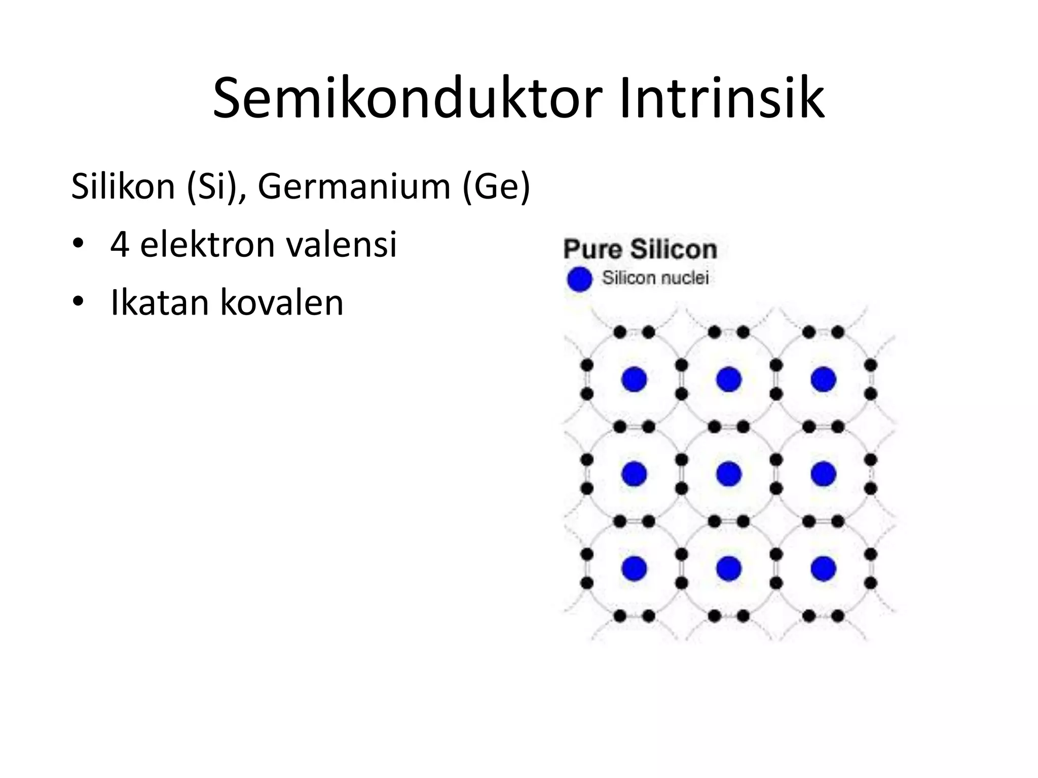
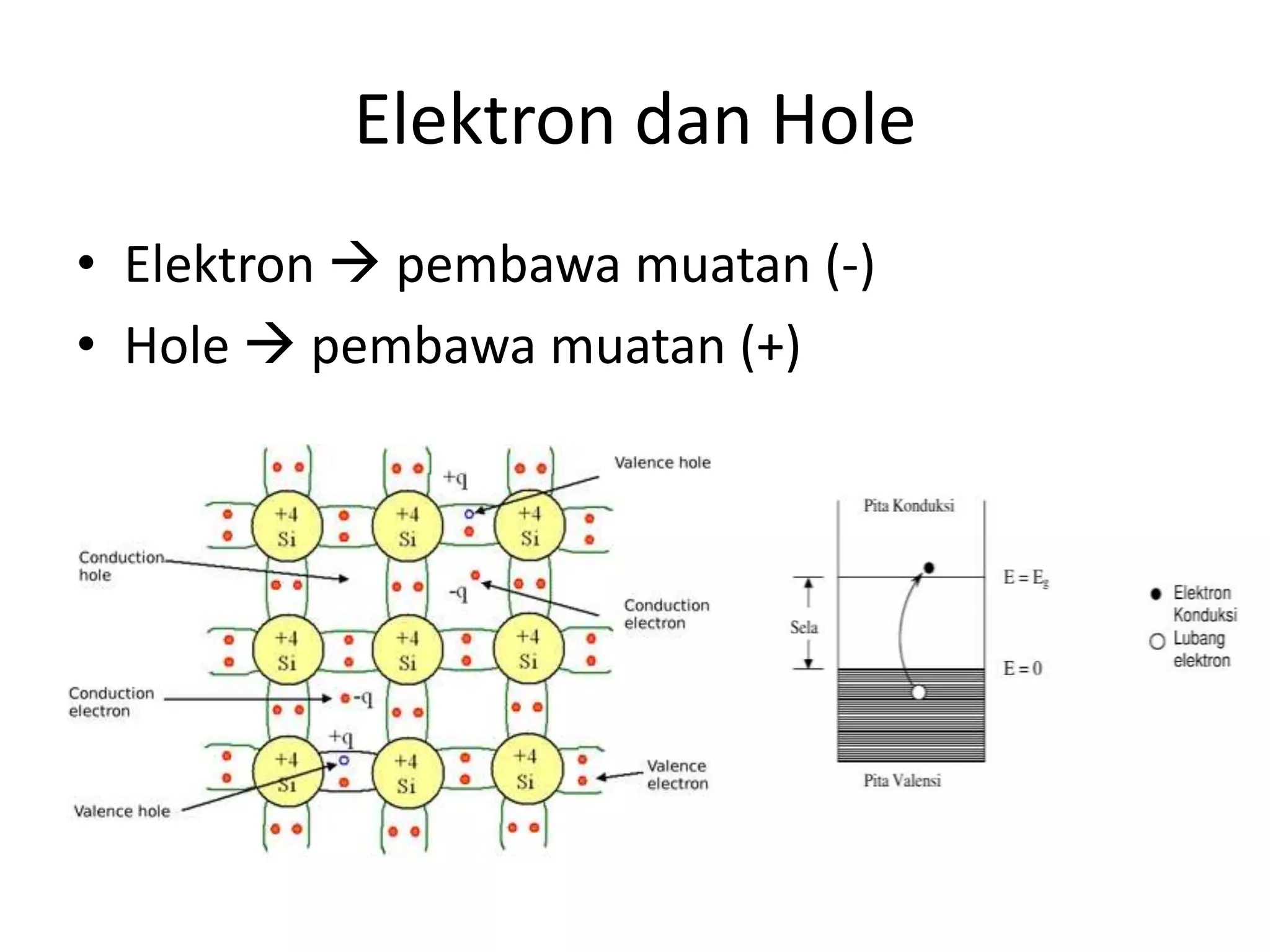
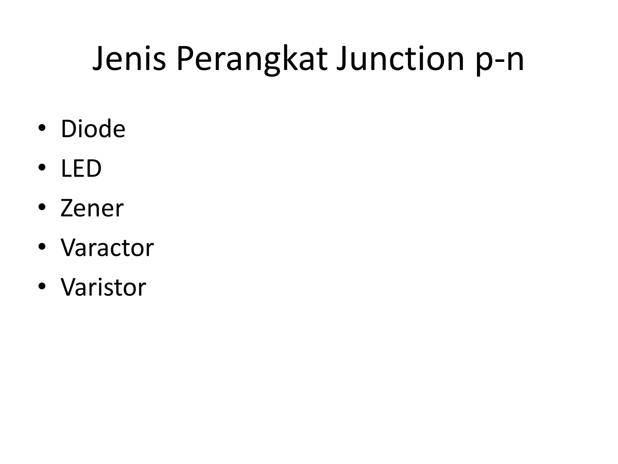
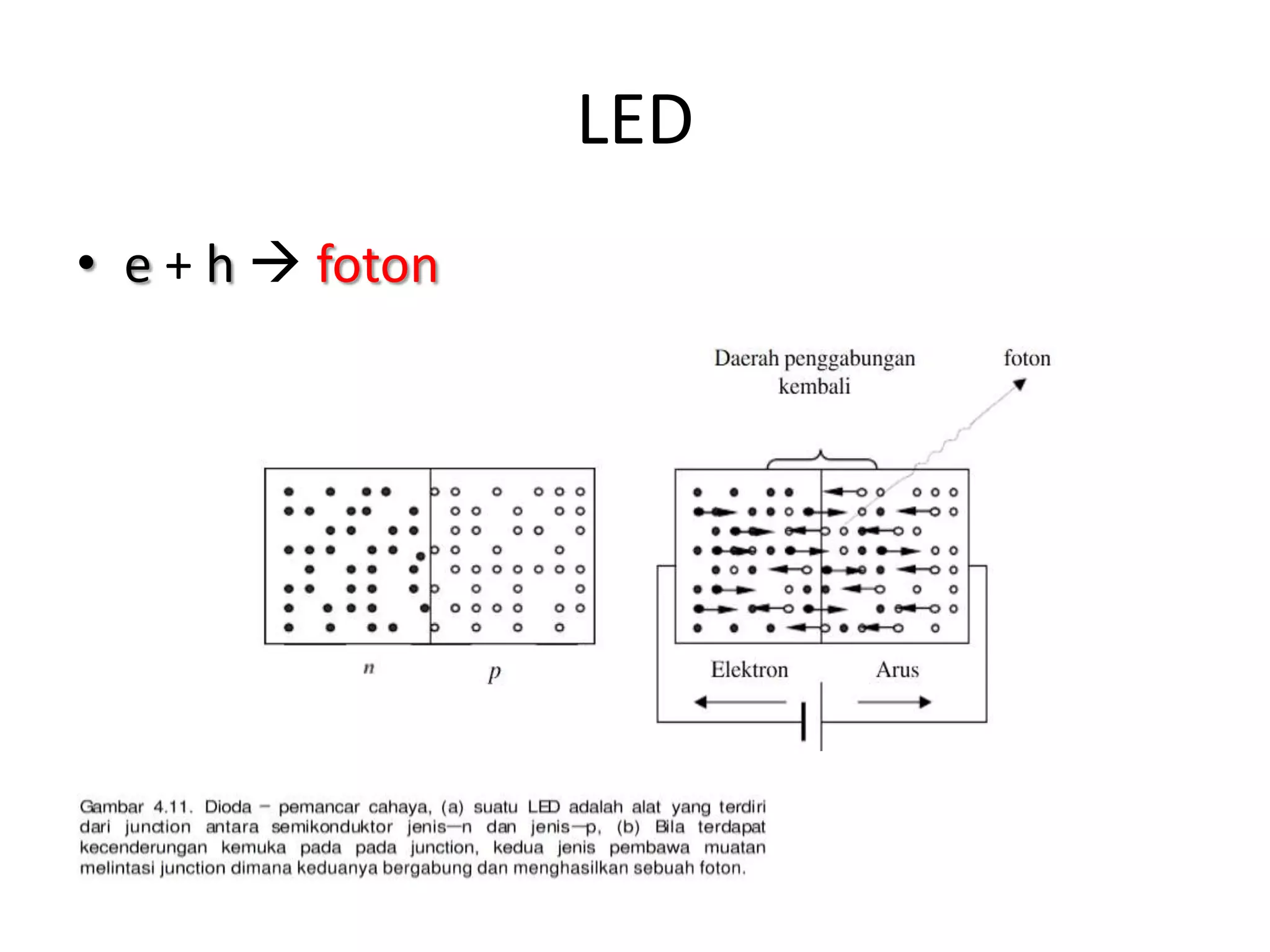
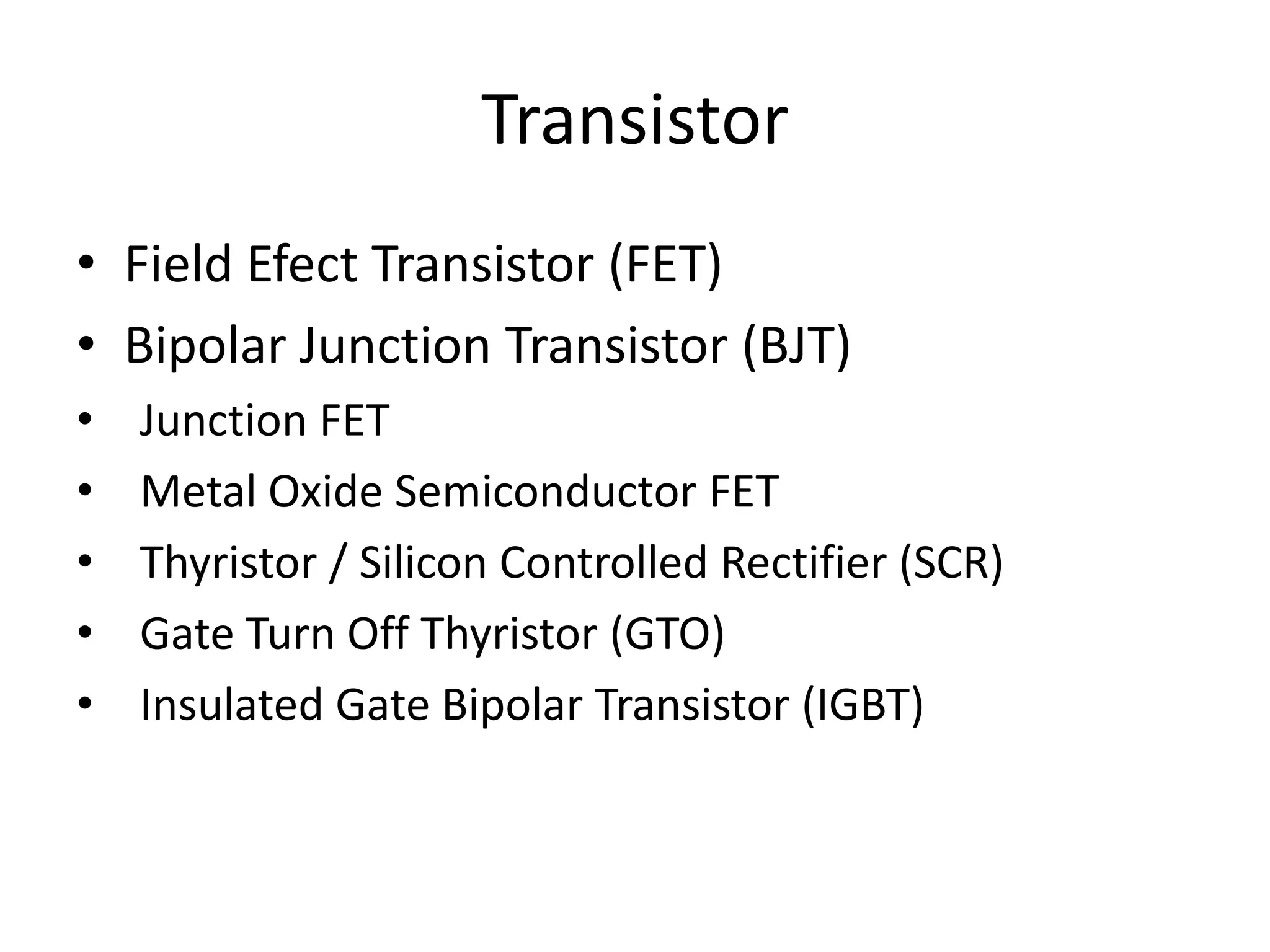

Dokumen ini menjelaskan tentang material semikonduktor, termasuk karakteristik semikonduktor intrinsik dan ekstrinsik, serta peran elektron dan hole sebagai pembawa muatan. Selain itu, menjelaskan perangkat semikonduktor seperti dioda, transistor, dan LED, serta prinsip dasar di balik fungsi mereka, seperti biasing dan konduktivitas. Contoh soal juga disertakan untuk memperjelas konsep-konsep yang dibahas.


![Pbl[1]](https://cdn.slidesharecdn.com/ss_thumbnails/pbl1-140917003315-phpapp01-thumbnail.jpg?width=640&height=640&fit=bounds)


